Article

Enhancing the Tunable Sensitivity of a Near-Ultraviolet to Visible to Near-Infrared Photo Irradiance Sensor Using an Indium Tin Oxide-Aluminum Oxide-Zirconia Aluminum Oxide-Silicon

1
Department of Semiconductor and Electro-Optics Technology, Minghsin University of Science and Technology, Xinfeng 30401, Taiwan
2
Department of Electronic Engineering, Minghsin University of Science and Technology, Hsinchu 30401, Taiwan
*
Author to whom correspondence should be addressed.
Crystals 2023, 13(11), 1530; https://doi.org/10.3390/cryst13111530
Submission received: 6 September 2023 / Revised: 18 October 2023 / Accepted: 18 October 2023 / Published: 24 October 2023
(This article belongs to the Special Issue Optoelectronics and Photonics in Crystals)

Abstract

:
This study focuses on enhancing the tunable sensitivity of a photo irradiance sensor (PIS) operating in the near-ultraviolet to visible to near-infrared (NUV-VIS-NIR) spectrum using an indium tin oxide-aluminum oxide-zirconia aluminum oxide-silicon oxide-silicon capacitor (hereafter IAZAOS). Unlike other PIS designs such as reverse-biased metal–insulator–semiconductor (MIS) and tunneling MIS, the IAZAOS PIS measures changes in inversion capacitance under strong forward bias with light irradiation. The IAZAOS PIS offers several key advantages over alternative designs. It exhibits high sensitivity, weak bias dependence, low dark current, tunable sensitivity, low power consumption, CMOS process compatibility, simple low-cost manufacturing, and good gate oxide reliability. Under 1 mW/cm2 irradiation at 1 kHz, the inversion carrier concentration reaches approximately 70% saturation. The resolution achieved is 10 nW/cm2 at 1 kHz, with a sensing range spanning from 10 nW/cm2 to 1 W/cm2 across frequencies from 1 kHz to 100 kHz. These performance characteristics surpass those reported for other PIS technologies. Furthermore, the IAZAOS PIS demonstrates a quantum efficiency of about 60% at 405 nm, which surpasses the quantum efficiency of general silicon-based p(i)n diodes. Post-deposition annealing techniques are employed to enhance the sensor’s performance. Dielectric annealing improves the ZrAlOx interface trap and permittivity properties, while conducting oxide annealing enhances indium tin oxide transmission and resistivity. The combination of these treatments results in a high-speed, high-sensitivity, high-resolution, and reliable NUV-VIS-NIR sensing capability for the IAZAOS capacitor-based PIS.

1. Introduction

Photo-detection across the ultraviolet (UV), visible (VIS), and infrared (IR) spectra plays an important role in many areas of science and technology. The near UV (NUV) region from 320 to 400 nm finds applications in chemical monitoring, biological sensing, missile plume detection, and exposure monitoring due to its ability to provide material and molecular identification. The visible spectrum from 400 to 700 nm is especially significant due to its prevalence in solar radiation at the Earth‘s surface. Human and animal vision have evolved to be most sensitive to visible light, underscoring its importance for imaging, displays, and general illumination applications. Advancing visible light photo-detection is critical due to our reliance on optical technologies centered in this range. Near-infrared (NIR) light from 700 to 1000 nm also has widespread utility, including uses in optical interconnects, fiber optic telecommunications, and night vision systems. Its properties of transmitting through many materials but not being visible to the human eye make NIR well suited for applications like spectroscopy, imaging, and sensing where optical access is needed but visibility is not required. The development of photo-detectors capable of responding across NUV-VIS-NIR regions has benefited many areas of science, industry, and daily life. This makes ongoing research into expanding the spectral detection ranges and improving the performance of photodetectors an important endeavor [1,2].

1.1. Three Common Types of Semiconductor-Based Photo Irradiance Sensors

There are three main structures used for photo irradiance sensors (hereafter PIS): p-i-n (PIN), metal–semiconductor–metal (MSM), and metal–insulator–semiconductor (MIS):
  • The PIN PISs consist of an intrinsic semiconductor layer sandwiched between p-doped and n-doped regions. This creates a built-in electric field across the intrinsic region; a reverse bias can further increase this field, causing photo-generated electron–hole pairs to separate. Carrier collection then enables light detection [3].
  • MSM PISs function on a similar principle, with the electric field distributed inside the semiconductor region. When illuminated, electron–hole pair generation and separation in the field allow photocurrent generation [4].
  • MIS PISs incorporate an insulator layer between the metal contact and the semiconductor. A deep-depletion region formed in the semiconductor of the MIS detector can provide the electric field for the separation of photo-generated electron–hole pairs. Electron–hole pairs created in the depletion region are collected, enabling photodetection. Compared to PIN, the MIS structure has a simpler fabrication process without doping requirements. It also benefits from a lower dark current than MSM detectors due to the insulator layer between the metal and semiconductor [5].
Reverse bias electric fields were applied to these three common photodetectors to separate and collect photo-generated carriers.

1.2. TCO-High-k-Si Capacitor PIS

In this work, we present a novel NUV-VIS-NIR PIS based on a transparent conducting oxide-high-k dielectric-semiconductor capacitor (hereafter THSC) structure. The high-k dielectric provides high-speed capabilities, the transparent conducting oxide (TCO) gate offers high transmission in the NUV-VIS-NIR range, and silicon provides a suitable bandgap for absorption of NUV-VIS-NIR. The THSC capacitor enables high-speed, high-sensitivity, and high-resolution of the IAZAOS PIS.
Using transparent conductive oxide TCO instead of Al as the MIS gate electrode, the photon can directly pass through the TCO to generate a photocurrent in the semiconductor, which can increase the photoresponse. This allows photons to generate electron–hole pairs over a greater interaction region within the semiconductor’s depletion layer, rather than only at the device edges [6]. Silicon is a highly promising material for NUV-VIS-NIR detection due to its bandgap of 1.12 eV. Additionally, silicon is abundantly available on Earth. Silicon-based MIS PIS could readily be integrated with ultra-large-scale integrated circuits, leveraging existing silicon semiconductor manufacturing infrastructure and processes. Using high-k materials, the time to generate light-induced charge becomes faster [7,8,9,10,11].
Unlike conventional reverse bias-type metal–insulator–semiconductor (MIS) PIS, our THSC PIS operates in the forward bias and measures the changes in strong inversion capacitance under a strong inversion gate bias with light irradiation. Compared with reverse bias MIS PIS, THSC PIS has high sensitivity and a low dark signal. The THSC structure lacks a source and a drain, so inversion carriers cannot be supplied independently of light generation. However, the light-induced inversion capacitance (hereafter LINC) of the THSC varies significantly with increasing photo irradiance (E), due to the corresponding rise in light-generated inversion carrier concentration.
Unlike tunneling-type MIS sensors, which rely on thin-gate oxide tunneling photocurrent, the THSC PIS exhibits good endurance due to its low-voltage operation at VG 1.5 V, which avoids gate dielectric leakage and breakdown. Additionally, the THSC sensitivity can be tuned by measuring the capacitance–voltage (C–V) characteristics at different frequencies. This is because the LINC response changes under fixed illumination as the measuring frequency is varied.
In summary, the key advantages of the THSC PIS include: 1. High sensitivity 2. Weak bias dependence; 3. Sensitivity tunable; 4. Low power consumption; 5. Good endurance; 6. CMOS process compatibility; 7. Simple low-cost manufacture; 8. NUV-VIS-NIR sensing range; 9. Low dark current [7,8].
This article uses the ITO-Al2O3-ZrAlOX-SiO2-Si capacitor (hereafter IAZAOS) as NUV-VIS-NIR THSC PIS. This article explores the use of Si-based THSC PIS with a combination of nanocrystalline high-k dielectric ZrAlOX (ZAO) and nanocrystalline TCO indium tin oxide (ITO) for achieving high performance in NUV-VIS-NIR THSC PIS. This paper introduces a new high-k material, ZrAlOx, HfAlOx, for THSC PIS, which is different from other high-k materials discussed in the other article [7,8]. This paper studies the performance comparison of IAZAOS and ITO-Al2O3-HfAlOX-SiO2-Si (hereinafter IAHAOS) as THSC PIS. LINC variations were compared under various CV measuring frequencies. LINC variations were also compared under various post-dielectric annealing (PDA) and post-gate conductor annealing (PMA). The permittivity, interface trap, and gate leakage characterizations of IAZAOS and IAHAOS after the PDA process are studied. The light transmission and resistivity of indium tin oxide after the PDA process are also studied. Analysis suggests IAZAOS sensitivity depends on high-k material properties (permittivity, gate leakage, and interface traps) and ITO film characterization (optical transmission and electrical resistivity). The combination of PDA ZrAlOx and PMA ITO enables high-speed, high sensitivity, and high-resolution of the IAZAOS PIS [9,10,12,13,14,15].
As shown in Table 1, four semiconductor-based PISs are compared [3,4,5].

2. Materials and Methods

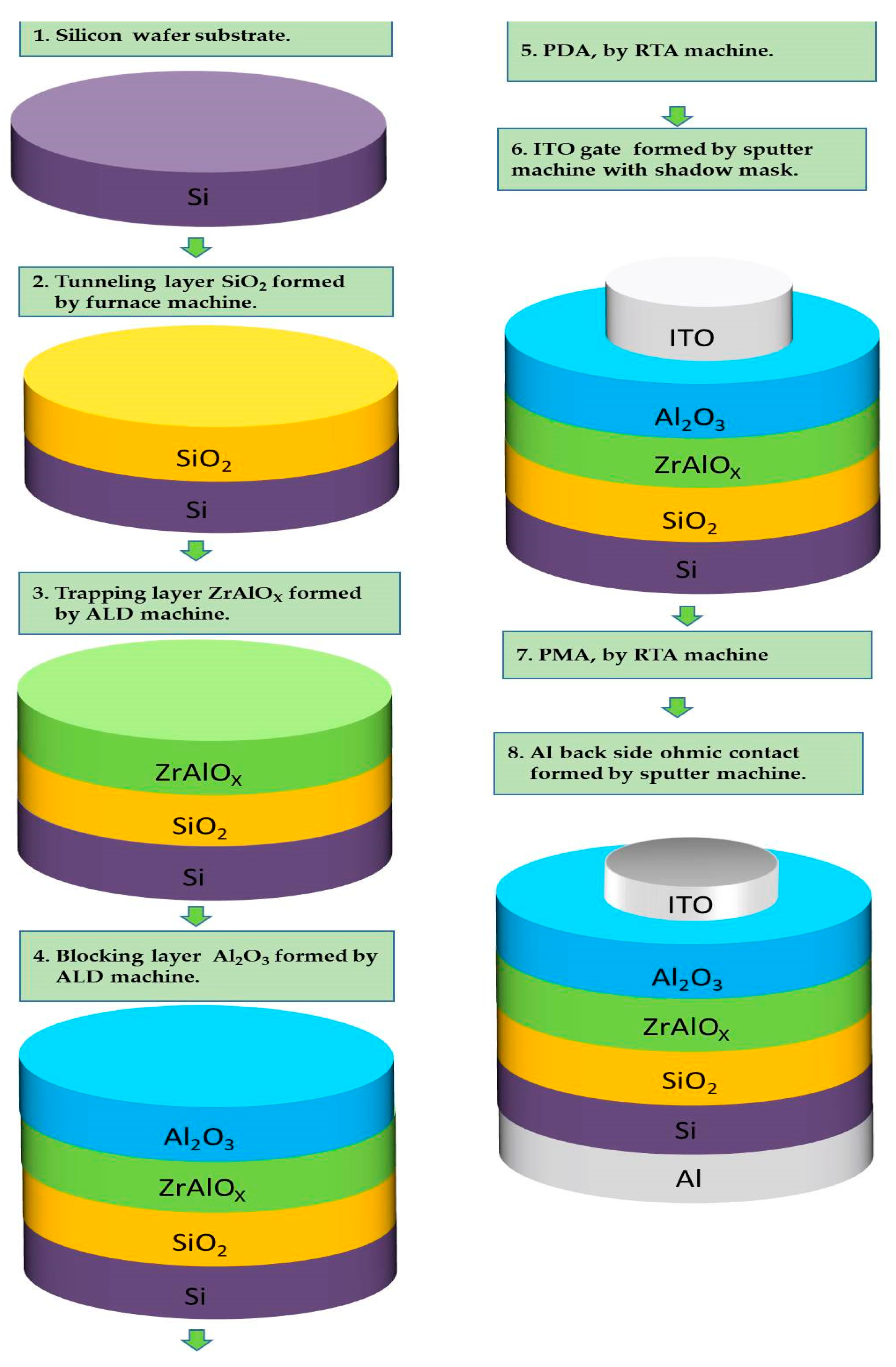
2.1. Sensor Design and Materials

The top-view optical microscope (OM) image of the IAZAOS irradiance sensor is shown in Figure 1. The 3D fabrication process flow of the IAZAOS capacitor photo irradiance sensor (PIS) is illustrated in Figure 2. Detailed information on the IAZAOS PIS manufacturing process can be found elsewhere [9]. The whole manufacturing process was si-based for CMOS process compatibility.
The design of the IAZAOS capacitor sensor took into account several factors regarding the selection of elements and the thickness of different layers within the system, as well as their interplay. The following considerations were made:
  • Substrate Selection: p-Silicon (100) (15–25 Ω-cm) was chosen as the substrate material for NUV-NIR light absorption and carrier generation.
  • Bottom Dielectric: A 3–5 nm SiO2 layer was implemented as the bottom dielectric to minimize interface defects of ZrAlOx and leakage current from ZrAlOx. The thin bottom dielectric also served the purpose of additional substrate path tunneling for the carrier generated by ZrAlOx under light. SiO2 is optically transparent in the NUV-NIR range.
  • Middle Dielectric: A 5–15 nm high-k ZrAlOx layer, with a thickness ranging from 5 to 15 nm, was utilized as the middle dielectric. This high-k choice aimed to enhance the speed of the sensor. Additionally, Al-doped ZrO2 was incorporated into this layer to further reduce leakage. Smaller nanocrystalline particles were seen in the ZrAlOx; these might be interpreted as light absorption and carrier production.. ZrAlOx is optically transparent in the NUV-NIR range.
  • Top Dielectric: A 10–20 nm high-k Al2O3 layer, with a thickness of 10–20 nm, was employed as the top dielectric. This high-k choice aimed to enhance the speed of the sensor. This thick Al2O3 layer served the purpose of gate leakage reduction in ZrAlOx for the gate tunneling path. Al2O3 is optically transparent in the NUV-NIR range.
By carefully selecting these elements and determining the appropriate thickness for each layer, the IAZAOS capacitor sensor was designed to optimize performance and minimize leakage effectively.
In this study, each layer structure of IAZAOS/IAHAOS had the same thickness to facilitate photocapacitance sensor response performance comparison. As shown in Table 2, we fabricated six IAZAOS/IAHAOS sensors with different post-deposition anneal (PDA) and post-metallization anneal (PMA) conditions to compare the photocapacitance sensor response performance of devices with different PDA and temperature PMA.

2.2. THSC PIS Operation Flow

The operation flow of THSC PIS can be described as follows: (1) Data Erase: Before writing data, the THSC PIS should be erased first to eliminate the interface and border trap charges trapped in the THSC PIS due to the influence of the natural environment, so that the C–V curve without interface and border charge effects can be inspected. By injecting positive charges under pulse negative (for p-substrate) gate bias VG, the data in the THSC PIS can be erased to the null state. (2) Data Write and Read: We used the HP4284 C–V curve meter to measure the C–V curve under various measuring frequencies with photo irradiation. The variation in LINC characterization can be inspected in the 1 kHz–100 kHz C–V curve with photo irradiation. The variations in LINC were compared under various photo irradiation conditions, various measuring frequencies, and various devices. Table 3 lists various irradiance E, measuring frequencies, and wavelength conditions for the IAZAOS irradiance sensor. The 6-wavelength module LED sources (with wavelengths of 365 nm, 405 nm, 475 nm, 565 nm, 625 nm, and 780 nm) (THORLABS, CHROLIS-C1) were employed in the experiments.

2.3. IAZAOS PIS Material Inspection

This study employed four techniques for IAZAOS PIS material analysis:
  • Material crystallinity was observed using transmission electron microscopy (TEM) (JEOL JEM-2010F, Tokyo, Japan);
  • Material crystallinity was observed using X-ray diffraction (XRD) (PANalytical X’Pert Pro);
  • For material transmission qualities, optical spectroscopy (Shimadzu-UV-250) was utilized;
  • The Olympus-BX63 optical microscope (OM) was used for top-view IAZAOS PIS imaging.

3. Results

3.1. LINC Increases in IAZAOS

Figure 3a–c displays the C–V curve of the IAZAOS-I2Z2 with different photo irradiances under W405K1, W405K10, and W405K100 irradiation conditions, respectively. The inversion characterization can be inspected in the C–V curve with light but cannot be inspected in the C–V curve without light, in agreement with former studies [7,8]. The variation in LINC increases with the decrease in frequency, as shown in Figure 3a–c, respectively. Under illumination conditions of W405K1L5, the measured LINC at a VG of 1.5 V was approximately 0.9 times the value of the accumulative capacitance (ACC) recorded at a VG of −2.5 V. This suggests that the inversion carrier concentration under such irradiation reached around 90% of saturation level [7,8,12,13,14,15].
Figure 4a–c illustrates the correlation between the increase in LINC change and the increase in photo irradiance for an IAZAOS-I2Z2 sensor under the W405K1, W405K10, and W405K100 irradiation conditions, respectively. The normalized inversion capacitance variation is calculated as the difference between LINC (VG 1.5 V) and the dark inversion capacitance (VG 1.5 V), divided by the difference between the ACC (VG −2.5 V) and the dark inversion capacitance (VG 1.5 V). The normalized inversion capacitance change was nearly zero without light irradiation and was nearly one under W405L10K1, W405L100K10, and W405L1000K100 irradiation conditions, as shown in Figure 4a–c, respectively. The LINC increased as a function of photo irradiance for the IAZAOS PIS, but the LINC increased more slowly when photo irradiance was greater than 3, 30, and 300 mW/cm2 under 1 kHz, 10 kHz, and 100 kHz measurements.
Figure 5a,b displays the C–V frequency dispersion for IAHAOS-I2H1 and IAZAOS-I2Z2 under the W405L0 irradiation condition. Figure 5c displays the C–V comparison of IAHAOS-I2H1, IAZAOS-I2Z2, and IAZAOS-I2Z1 under the W405L0K1 irradiation condition. The IAHAOS device shows greater frequency dispersion in the depletion region compared to the IAZAOS device. The IAZAOS-I2Z2 device shows the highest accumulative capacitance compared to the IAZAOS-I2Z1 and IAHAOS-I2H1 devices. The C–V frequency dispersion characterization for high-k material ZAO/HAO is consistent with former studies [16,17,18].

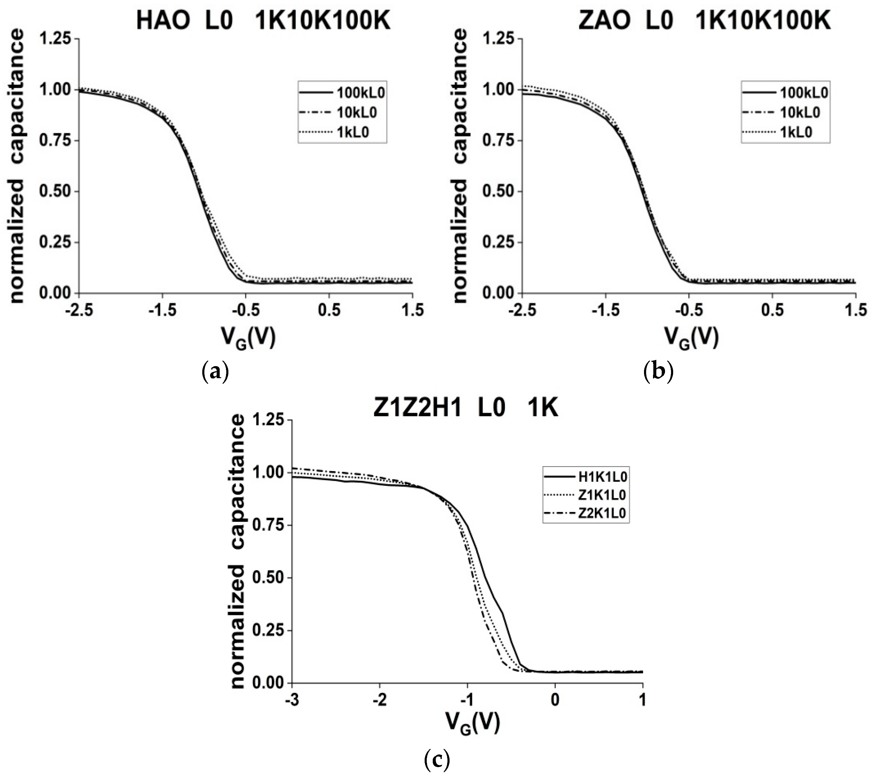
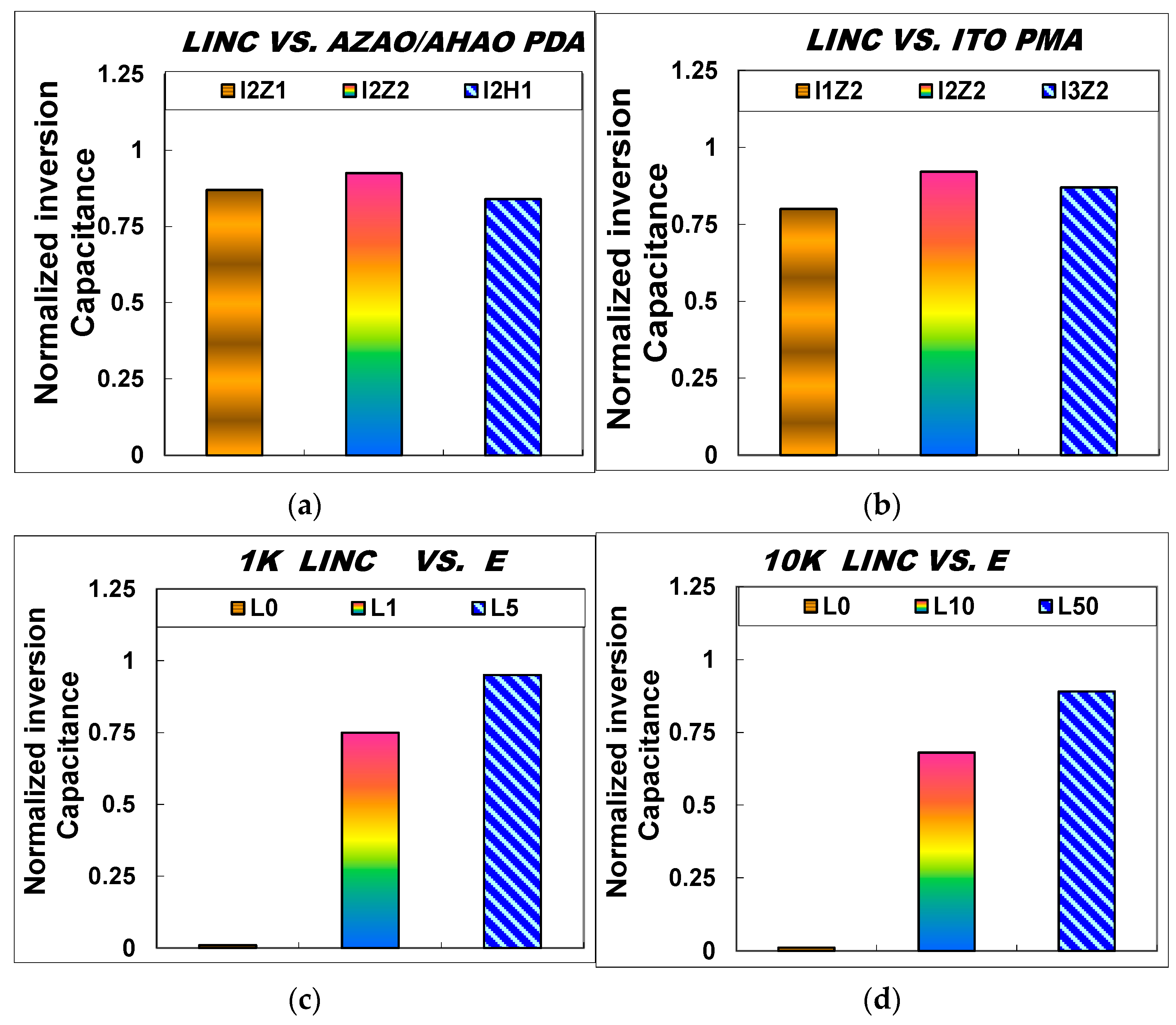
3.2. LINC Comparison for Various IAZAOS at Different UV Wavelengths and Different Annealing Temperatures

In Figure 6a, a comparison of the LINC change (at VG 1.5 V) is presented for various IAZAOS/IAHAOS capacitor devices with different PDA anneal temperatures after exposure to the W405L5K1 irradiation condition. It is observed that the LINC change (at VG 1.5 V) of IAZAOS-I2Z2 is greater than that of IAZAOS-I2Z1 and IAHAOS-I2H1 devices under the W405L5K1 irradiation condition. It is also found that the LINC change of IAHAOS-I2H1 is smaller compared to that of IAZAOS-I2Z1 under the W405L5K1 irradiation condition.
A comparison of the LINC change (at VG 1.5 V) for various IAZAOS capacitor devices with different PMA temperatures after exposure to the W405L5K1 irradiation condition is depicted in Figure 6b. It is observed that the LINC change (at VG 1.5 V) of the IAZAOS-I2Z2 device was most significant compared to the IAZAOS-I1Z2 and IAZAOS-I3Z2 devices after exposure to the W405L5K1 irradiation condition.
Figure 6c–e displays a comparison of the LINC (at VG 1.5 V) change for IAZAOS-I2Z2 with different photo irradiances under the W405K1, W405K10, and W405K100 irradiation conditions, respectively. The LINC (at VG 1.5 V) increased nearly over 0.9 times ACC when photo irradiance was greater than 5, 50, and 500 mW/cm2 under 1 kHz, 10 kHz, and 100 kHz measurements [19,20].
A comparison of the CVSILC for the IAZAOS and IAHAOS devices is shown in Figure 6f. It is observed that the CVSILC of the IAHAOS-I2H1 device was almost 1000 times greater than that of the IAZAOS-I2Z2 at –4 V VG 100 s. Moreover, the CVSILC of the IAHAOS-I2H1 device at –4 V VG 100 s was nearly 1 μA, while the CVSILC of the IAZAOS-I2Z2 device at –4 V VG 100 s was less than 1 nA. The CVSILC characterization for high-k material is consistent with former studies [21,22,23,24,25].
Figure 6g provides a comparison of LINC changes in the IAZAOS-I2Z2 under different irradiation wavelengths under L50K10 irradiation conditions. When the light irradiance is 625 nm, 405 nm, and 365 nm, LINC (VG 1.5 V) is close to 0.98, 0.87, and 0.6 times of ACC, respectively.

3.3. Photo Transmittance and Resistivity Comparison of ITO Films at Different Annealing Temperatures

Figure 7a shows the transmittance spectra of ITO films annealed at different temperatures, measured over wavelengths from 200 to 900 nm. Figure 7b compares the transmittance at 405 nm wavelength; the I2 sample demonstrated superior performance compared to I1 and I3. Figure 7c provides the transmittance values for the optimized I2 sample across relevant photo wavelengths. Notably, the I2 ITO film achieved transmittance of 95% at 405 nm, over 80% at 780 nm, 625 nm, 565 nm, and 475 nm, and around 75% at 365 nm. Figure 7d compares the electrical resistivity of ITO films subjected to different annealing temperatures. The I2 sample exhibited the lowest resistivity, indicating improved electrical characteristics from the post-metallization thermal treatment. These transmittance and resistivity results validate that annealing temperature optimizes the ITO film properties, in agreement with previous reports [26,27]. Overall, sample I2 processed with intermediate annealing displayed the best combined optical and electrical performance suitable for the photo irradiance sensor application [28,29].

3.4. XRD and TEM Comparison of ITO Films at Different Annealing Temperatures

Figure 7e shows the comparison of the X-ray diffraction (XRD) patterns of ITO films at different annealing temperatures. The ITO sample exhibits a series of XRD peaks at 2θ = 30.26°, 35.38°, 45.42°, 51.10°, and 60.72°, corresponding to the (2 2 2), (4 0 0), (4 3 1), (4 4 0), and (6 2 2) planes of the standard ITO (JCPDS No. 71-2195), respectively. XRD analysis shows that the crystallization process of the ITO film depends on temperature, and ITO undergoes phase transformation during the PMA process. This is due to the fact that the intensity of the (2 2 2) XRD diffraction peak of the ITO film increases with the increase in PMA [26,30,31].
Figure 8a–c shows transmission electron microscopy (TEM) images comparing the crystal structure of ITO films subjected to different post-metallization annealing (PMA) temperatures. The TEM analysis revealed that sample I1-ITO exhibited an amorphous structure mixed with incomplete nano-columnar (NCols) grains. In contrast, sample I2-ITO displayed more complete and elongated NCols grains. Sample I3-ITO featured wider but shorter columnar grains. These TEM observations of changing ITO crystallinity with annealing temperature are consistent with previous reports [32,33,34,35].
Figure 8d–f shows a TEM comparison of ZrAlO (ZAO) and HfAlO (HAO) films after various post-deposition annealing (PDA) temperatures. The TEM results indicate that sample ZAO-Z1 remained nearly amorphous, while sample ZAO-Z2 exhibited partially smaller nano-crystallized regions. In comparison, sample HAO-H1 showed a larger nano-crystallized structure. The impact of PDA temperature on high-k film structure characterization by TEM agrees with past studies [22,23,24,25]. Overall, the TEM analysis validated the influence of post-fabrication thermal treatments on material crystallinity.

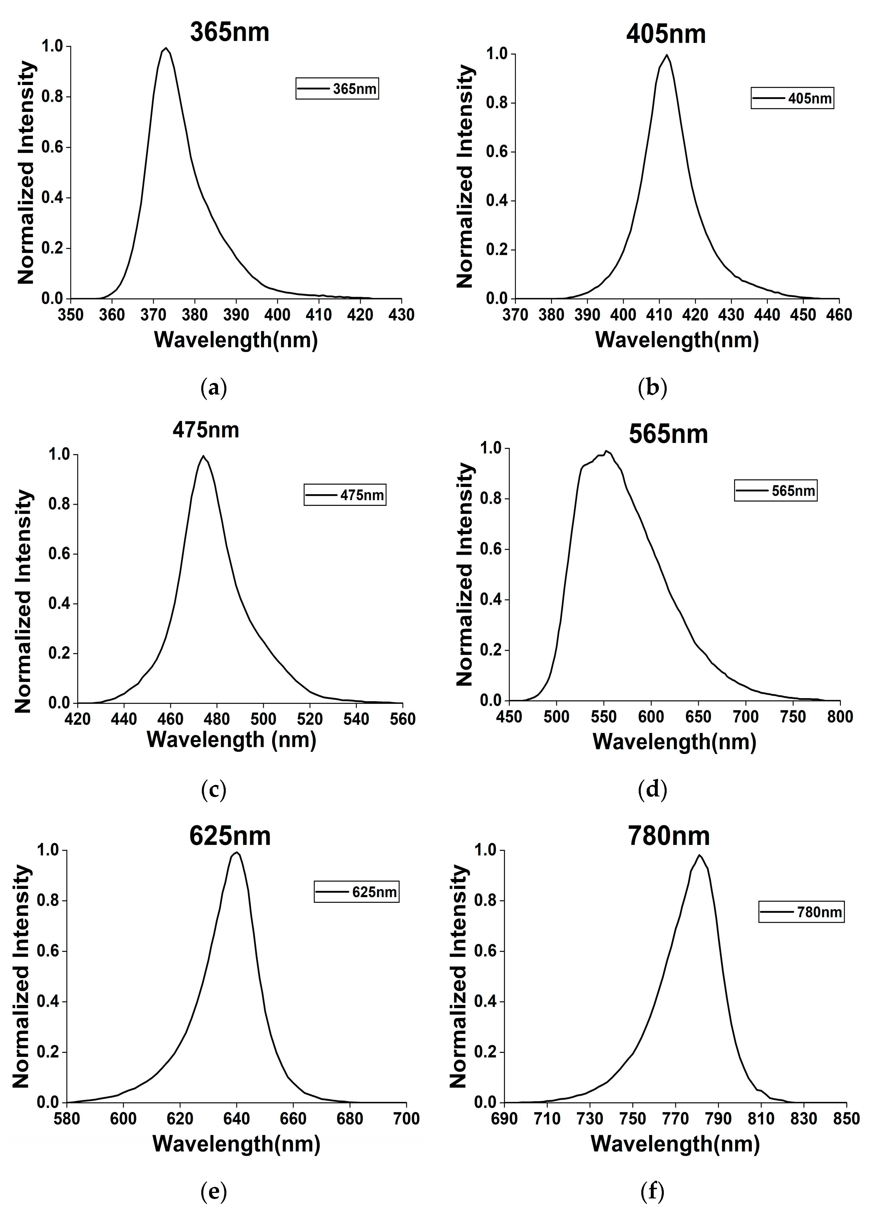
3.5. The Spectra for NIR-VIS-NUV LEDs

The spectral distribution of the 6-wavelength module LED light sources (with wavelengths of 365 nm, 405 nm, 475 nm, 565 nm, 625 nm, and 780 nm) used in this study is shown in Figure 9.

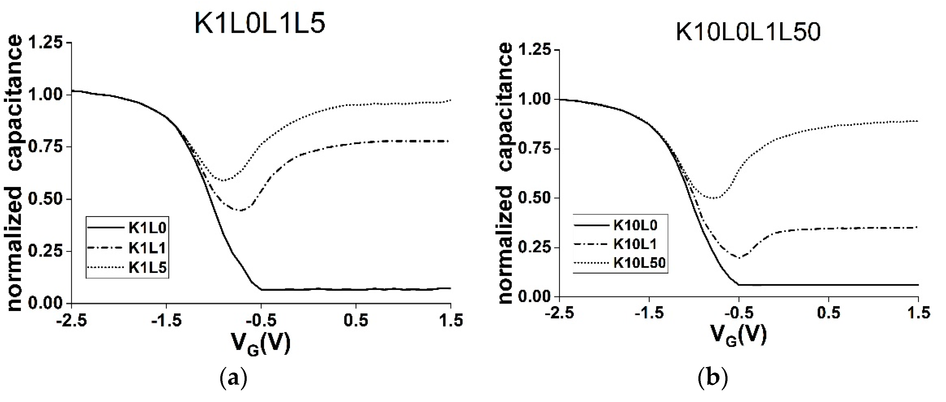
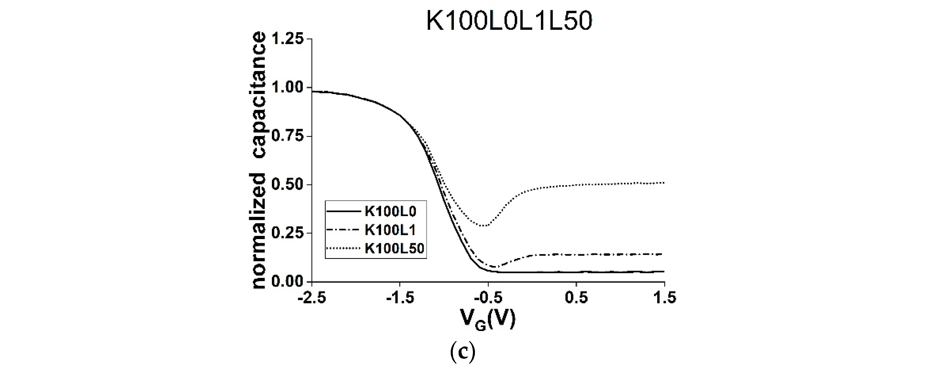
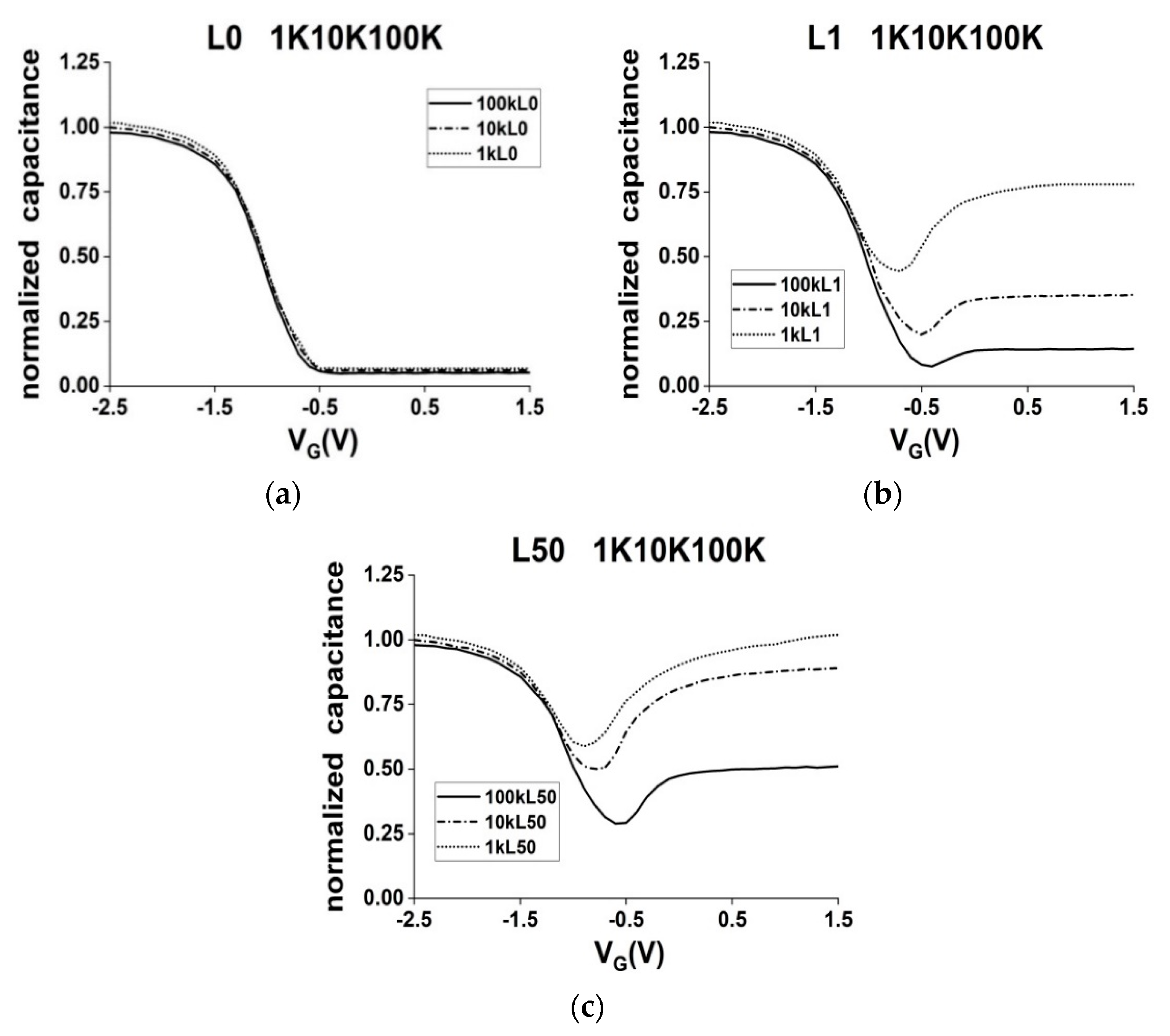
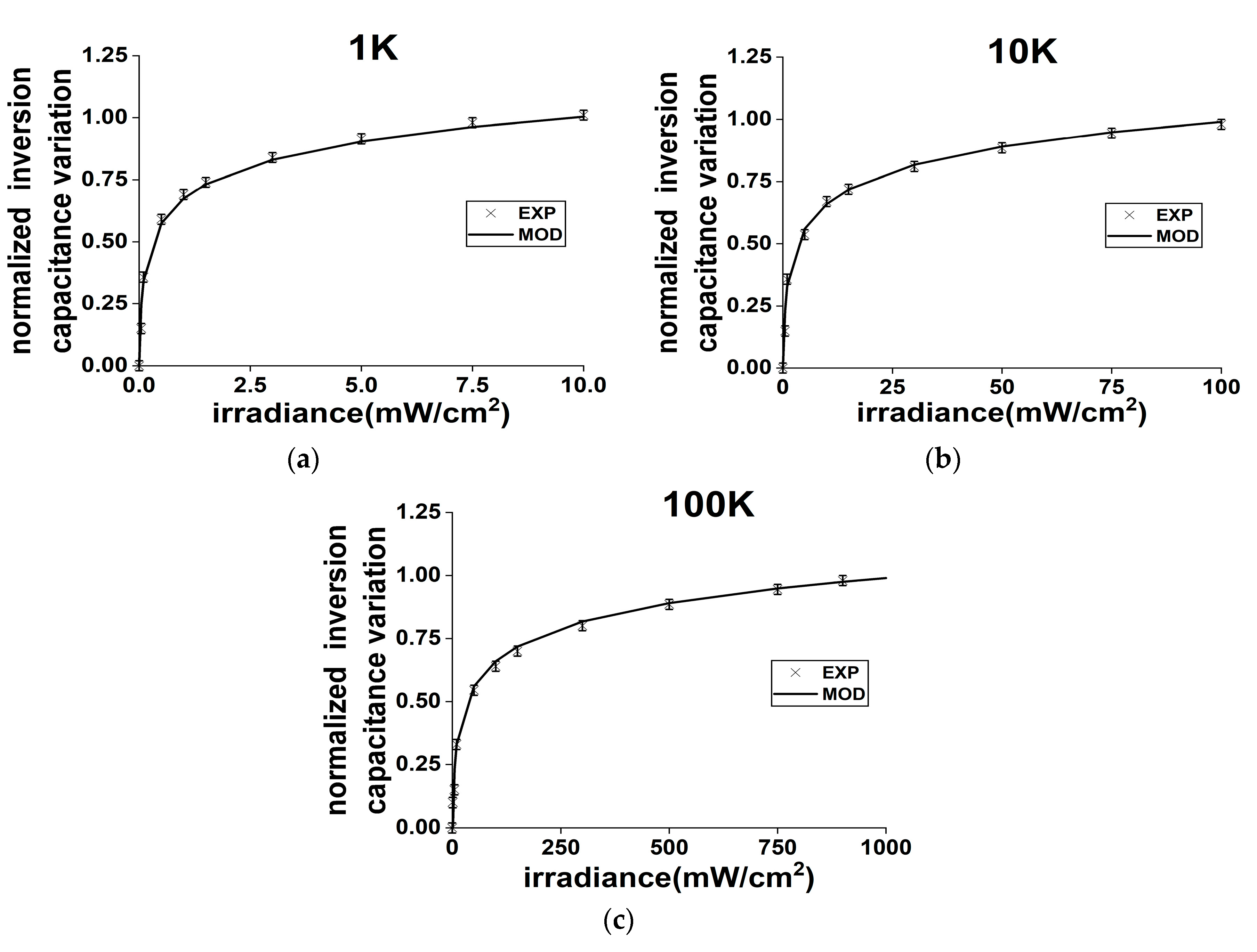
3.6. The Dependence of LINC on Different Measuring Frequencies

Figure 10a–c presents a comparison of the C–V comparison of IAZAOS-I2Z2 at different measurement frequencies under W405L0, W405L1, and W405L50 irradiation conditions. The variation in LINC increases with a decrease in frequency, respectively.

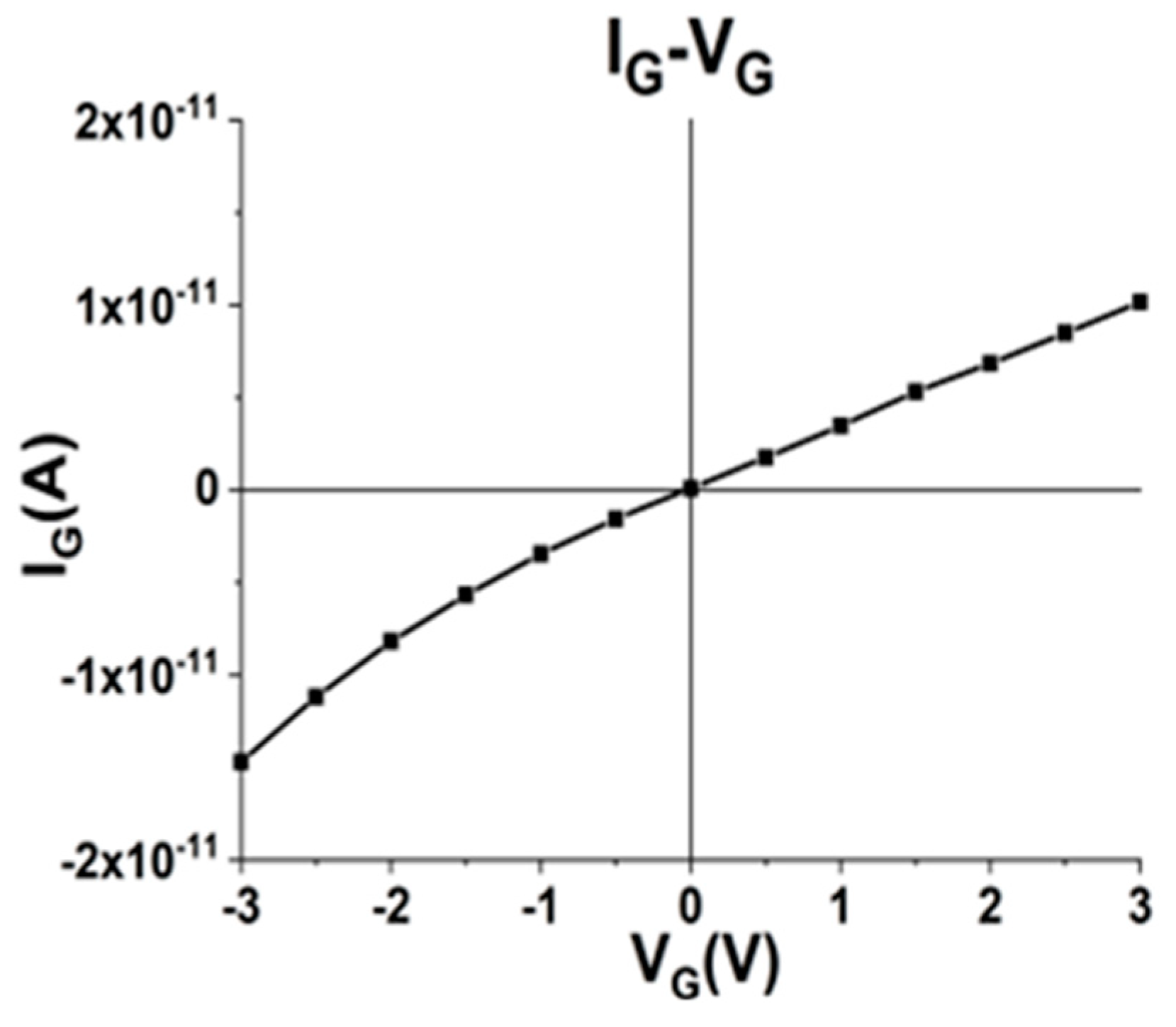
3.7. The I-V of the Device under Light Illumination

Figure 11 shows the IG-VG curve of the IAZAOS-I2Z2 device under light illumination. Unlike reverse-biased MIS and tunneled MIS PIS, the gate leakage is very small and does not change whether there is light or no light.

3.8. The Photocapacitance Time Response of the IAZAOS PIS

Figure 12 shows the photocapacitance time response of the IAZAOS PIS under the W405L1 irradiation condition. The rise and fall times of the IAZAOS photocapacitance time response are small.

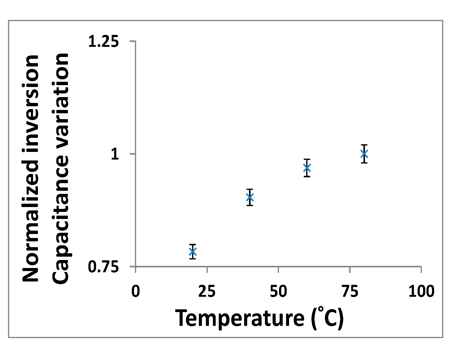
3.9. The Temperature Dependence of Photocapacitance Response for the IAZAOS PIS

Figure 13 shows the temperature dependence of the photocapacitance response for the IAZAOS PIS under the W405L1K1 irradiation condition. The LINC increases with increasing temperature.

4. Discussion

4.1. LINC Change in IAZAOS

The inversion characterization can be easily inspected in the 1 kHz–100 kHz C–V curve with light but is nearly invisible in the C–V curve without light, as shown in Figure 3. Photoionization generates a large number of electron–hole pairs in the lightly doped substrate, so that the minority concentration (negative charges) is significantly increased. The time to generate charge becomes shorter by photo ionization; therefore, the variations in LINC characterization are more easily inspected [7,8]. With the W405K1L5 irradiation condition, the inversion ratio (hereafter INCR), defined as the ratio of the LINC (VG = 1.5 V) to the ACC (VG = −2.5 V), was nearly 70% and 95% with 1 mW/cm2 and 5 mW/cm2 irradiation under 1 kHz measurement. The sensitivity was 705 INCR·cm2/W and 190 INCR·cm2/W with 1 mW/cm2 and 5 mW/cm2 irradiation under 1 kHz measurement. The results show that the IAZAOS PIS is very sensitive to photo irradiance compared to previous studies [7,8].
The IAHAOS-I2H1 device shows greater frequency dispersion in the depletion region compared to the IAZAOS-I2Z2 and IAZAOS-I2Z1 devices, suggesting a higher density of interface traps for IAHAOS-I2H1 compared to the IAZAOS-I2Z2 and IAZAOS-I2Z1, as shown in Figure 5. It was suggested that the smaller and more uniform grain size in the PDA ZrAlOx (ZAO) facilitates the diffusion of oxygen into the grain and regions nearby the grain boundaries, and reduces the concentration of oxygen-vacancy defects, so the interface defect is improved. The interface defect concentration in the IAZAOS is lower than that in the IAHAOS. Moreover, the higher accumulation capacitance of the IAZAO device compared to the IAHAOS points to a higher permittivity of the ZrAlOx compared to the HfAlOx. Previous studies are consistent with this analysis [12,13,14,15].
The IAZAOS-I2Z2 had the largest LINC change (at VG 1.5 V), and the IAHAOS-I2H1 had the smallest LINC change (at VG 1.5 V) (as shown in Figure 6a), which is closely related to the frequency dispersion in the CV curve of the IAZAOS/IAHAOS (as depicted in Figure 5). The LINC of the IAZAOS-I2Z2 is better than that of the IAHAOS-I2H1 (as shown in Figure 6a), which is also closely related to the higher GSILC of the IAHAOS-I2H1 (as shown in Figure 6g). According to the information provided, it suggests a higher density of interface traps for the IAHAOS-I2H1 compared to the IAZAOS-I2Z2 and IAZAOS-I2Z1 (analysis from Figure 5c), a higher permittivity of the AZAO–Z2 compared to the AZAO-Z1 and AHAO-H1 (analysis from Figure 5c), and a higher gate leakage current of the IAHAOS-I2H1 compared to the IAHAOS-I2Z2 (analysis from Figure 6f). The largest LINC of the IAZAOS-I2Z2 is suggested to be due to the highest permittivity of the AZAO-Z2. The smallest LINC of the IAHAOS-I2H1 is suggested to be due to the highest density of interface traps and higher gate leakage current for the IAHAOS-I2H1. It is suggested that the performance of THSC PIS can be influenced by the permittivity, gate leakage current, and interface traps characteristic of high-k ZAO material [16,17,18,19,20,22,23,24,25].
It is observed that the LINC change (at VG 1.5 V) of the IAZAOS-I2Z2 is the most significant compared to the IAZAOS-I1Z2 and IAZAOS-I3Z2 under the W405L5K1 irradiation condition, as illustrated in Figure 6b. From the TEM analysis in Figure 8, the I2-ITO with the longest and most complete NCols crystalline structure was observed to result in the highest transmitance due to having the longest and straightest photon-transmitting grains. Moreover, the I3-ITO with the largest grain size and lowest grain boundaries was observed to result in the lowest resistivity due to having the lowest resistance for the charge carriers tunneling through the barriers of the grain [9,10,11,30,31,32,33]. However, as a trade-off between optical and electrical characteristics, the IAZAOS-I2Z2 has the best improved performance of the inversion type THSC PIS. Previous studies [9,10,11,30,31,32,33] are consistent with this analysis.
The significant difference in GSILC between the IAHAOS-I2H1 and IAZAOS-I2Z2 is depicted in Figure 6f. It was suggested that the smaller and more uniform grain size in the Z2- ZrAlOx (ZAO) facilitates the diffusion of oxygen into the grain and regions nearby the grain boundaries after PDA. These diffused oxygen atoms can reduce the concentration of oxygen-vacancy defects and the gate leakage current. It is suggested that the oxygen-vacancy defect concentration in the Z2-ZAO is lower than that in the H1-HAO. Previous studies are consistent with this analysis. Moreover, previous studies have also shown that PDA ZAO has a lower gate leakage current as a gate oxide than PDA ZrO2. It was suggested that Al doping of ZrO2 films reduces the concentration of the gate oxide defects, owing to their large optical bandgap [22,23,24,25].

4.2. Sensitivity of IAZAOS-I2Z2

The sensitivity can be tuned by changing the measuring frequency for the C–V curve, as depicted in Figure 10. The variation in LINC increases with a decrease in the measuring frequency. A lower frequency LF is more suitable for small photo irradiation signals, and a higher frequency HF is more suitable for large photo irradiation signals [7,8] Based on the experimental results, the sensitivity is 705 INCR·cm2/W, 330 INCR·cm2/W, and 100 INCR·cm2/W with W405L1K1, W405L1K10, and W405L1K100 irradiation conditions. The resolution of the IAZAOS-I2Z2 can be less than 10 nW/cm2 with a 1 kHz measuring frequency. The sensing range of the IAZAOS-I2Z2 is estimated to be around 10 nW/cm2 to 1 W/cm2, with a 1 kHz to 100 kHz measuring frequency. The calculated quantum efficiencies of the IAZAOS PIS at 625 nm, 475 nm, 405 nm, and 365 nm are 75%, 70%, 60%, and 40%, respectively. The quantum efficiency of IAZAOS PIS is higher than that of general p(i)n silicon diodes (at 625 nm, 475 nm, and 405 nm, it is 60%, 50%, and 40%, respectively). This shows that ZrAlOX exhibits some smaller nanocrystalline particles, which are excited by light to generate a large number of carriers, helping to improve quantum efficiency.

4.3. Model for Photo-Induced LINC Shift

To simulate the LINC variation of the IAZAOS device, the author proposed a model (hereafter called the HWC-LINC model) derived from the prior studies of the HWC-UVTD model [9,10,11].
Normalized inversion capacitance variation:
= [ INC(E) − INC(0)]/[ACC − INC(0)] = [W × A]log(K × E)
The equation presented here consists of several variables. E represents the photo irradiance (mW/cm2), INC(E) is the inversion capacitance at VG 1.5 V under photo irradiance E, and INC(0) is the dark inversion capacitance at VG 1.5 V. ACC is the accumulative capacitance at VG −2.5 V. The HWC-LINC model used experimental curve fitting to derive two parameters: W,A, and K. Therefore, the K parameter represents the constants for inversion carrier generation, A is the constant for specific devices, and W is the constant for a specific photo wavelength.
K is a function of electrical frequency.
K = 110 × F−1.02
F is the C–V measuring frequency. A is equal to 0.35 for the IAZAOS-I2Z2 devices in this study. W is equal to 0.95 for the W405 irradiation condition in this study. Figure 14a–c shows the comparisons of the measured and simulated curves of LINC change versus light irradiance E for an IAZAOS-I2Z2 under W405K1, W405K10, and W405K100 irradiation conditions in this study.

5. Conclusions

The IAZAOS PIS has high performance in NUV-VIS-NIR. Unlike the common reverse type MIS, the IAZAOS PIS offers several key advantages: high sensitivity, weak bias dependence, low dark current, tunable sensitivity, low power consumption, CMOS process compatibility, simple low-cost manufacturing, and good gate oxide reliability. In contrast to the common tunneling type MIS sensors, IAZAOS exhibits good endurance due to its low operation voltage (VG 1.5 V) with negligible gate oxide tunneling.
Experimental results show sensitivity values of 705, 330, and 100 INCR·cm2/W for irradiation conditions of W405L1K1, W405L1K10, and W405L1K100, respectively. The resolution is 10 nW/cm2 at 1 kHz measurement frequency. The sensing range of the IAZAOS-I2Z2 is 10 nW/cm2 to 1 W/cm2 under a 1 kHz to 100 kHz C–V measuring frequency. This surpasses other reported photo irradiance sensors. Furthermore, the IAZAOS PIS demonstrates a quantum efficiency of about 60% at 405 nm, which surpasses the quantum efficiency of general silicon-based p(i)n diodes.
Post-deposition annealing improves IAZAOS performance by modifying ZrAlOx interface traps, gate leakage, and permittivity via PDA, as well as enhancing ITO optical transmission and resistivity with PMA. Analysis suggests IAZAOS sensitivity depends on high-k material properties (permittivity, gate leakage, and interface traps) and ITO film characterization (optical transmission and electrical resistivity). The combination of PDA and PMA results in high-speed, high-sensitivity, and high-resolution NUV-VIS-NIR sensing.
Key advantages of IAZAOS PIS are high sensitivity, low dark current, weak bias, tunable sensitivity, low power consumption, good endurance, CMOS compatibility, and simple low-cost manufacturing. Future work involves developing “virgin” IAZAOS sensors without initial erasing, as well as further sensitivity, reliability, and sensing range enhancements. Although the circuit design for obtaining the capacitor output signal is relatively complicated in actual applications, this problem can be solved with the help of new AI and IC technologies [36].

Author Contributions

Conceptualization, W.-C.H.; methodology, W.-C.H.; formal analysis, W.-C.H.; data curation, B.-M.C.; writing—original draft, W.-C.H.; writing—review and editing, M.-C.W.; visualization, Y.-S.L.; supervision, C.-C.T. All authors have read and agreed to the published version of the manuscript.

Funding

This paper was funded in part by the National Science Council project (NSC) (NSC 109-2635-E-159-001-) and the National Nano Device Laboratories project (NDL) (JDP112-Y1-052).

Data Availability Statement

Not applicable.

Acknowledgments

The author would also like to thank National Nano Device Laboratories (NDL), National Tsing Hua University (NTHU), and National Chiao Tung University (NCTU) for providing the instruments for wafer fabrication and testing.

Conflicts of Interest

The author declares no conflict of interest.

References

  1. Klijn, M.E.; Hubbuch, J. Application of ultraviolet, visible, and infrared light imaging in protein-based biopharmaceutical formulation characterization and development studies. Eur. J. Pharm. Biopharm. 2021, 165, 319–336. [Google Scholar] [CrossRef] [PubMed]
  2. Papalias, T.A.; Wong, M. Making sense of light sensors. EEtimes 2006, 7, 19. [Google Scholar]
  3. Kasper, E.; Oehme, M. High Speed Germanium Detectors on Si. Phys. Stat. Sol. C 2008, 5, 3144–3149. [Google Scholar] [CrossRef]
  4. Brennan, K.F.; Haralson, J.; Parks, J.W.; Salem, A. Review of Reliability Issues of Metal-Semiconductor-Metal and Avalanche Photodiode Photonic Detectors. Microelectron. Reliab. 1999, 39, 1873–1883. [Google Scholar] [CrossRef]
  5. Lee, H.C.; Su, Y.K.; Lin, J.C.; Cheng, Y.C.; Wu, S.L.; Jhou, Y.D. AlInGaN Metal-Insulator-Semiconductor Photodetectors at UV-C 280 nm. Electrochem. Solid-State Lett. 2009, 12, H357–H360. [Google Scholar] [CrossRef]
  6. Liu, C.W.; Liu, W.T.; Lee, M.H.; Kuo, W.S.; Hsu, B.C. A Novel Photodetector Using MOS Tunneling Structures. IEEE Electron Device Lett. 2000, 21, 307–309. [Google Scholar] [CrossRef]
  7. Yang, T.; Liu, Y.; Ye, P.D.; Xuan, Y.; Pal, H.; Lundstrom, M.S. Inversion capacitance-voltage studies on GaAs metal-oxide-semiconductor structure using transparent conducting oxide as metal gate. Appl. Phys. Lett. 2008, 92, 2105. [Google Scholar] [CrossRef]
  8. Sze, S.M.; Ng, K.K. Physics of Semiconductor Devices, 3rd ed.; John Wiley & Sons: Hoboken, NJ, USA, 2006; p. 663. [Google Scholar]
  9. Jong, F.C.; Hsieh, W.C. Performance Comparison of SONOS-Type UV TD Sensor Using Indium Tin Oxide-Aluminum Oxide-Zirconia Aluminum Oxide-Silicon Oxide-Silicon and Indium Tin Oxide-Aluminum Oxide-Hafnium Aluminum Oxide-Silicon Oxide-Silicon. Crystals 2023, 13, 1092. [Google Scholar] [CrossRef]
  10. Hsieh, W.C.; Jong, F.C.; Tseng, W.T. Performance Improvement of Total Ionization Dose Radiation Sensor Devices Using IOHAOS with Enhanced UV Transparency ITO Gate. Coatings 2021, 11, 408. [Google Scholar] [CrossRef]
  11. Hsieh, W.C. Performance Improvement of a Nonvolatile UV TD Sensor Using SAHAOS with a High Temperature Annealed, Partially Nano-Crystallized Trapping Layer. Sensors 2019, 19, 1570. [Google Scholar] [CrossRef]
  12. Rahman, M.M.; Kim, D.H.; Kim, T.W. Border Trap Characterizations of Al2O3/ZrO2 and Al2O3/HfO2 Bilayer Films Based on Ambient Post Metal Annealing and Constant Voltage Stress. Nanomaterials 2020, 10, 527. [Google Scholar] [CrossRef] [PubMed]
  13. Hlali, S.; Hizem, N.; Militaru, L.; Kalboussi, A.; Souifi, A. Effect of interface traps for ultra-thin high-k gate dielectric based MIS devices on the capacitance-voltage characteristics. Microelectron. Reliab. 2017, 75, 154–161. [Google Scholar] [CrossRef]
  14. Misra, D. High k dielectrics on high-mobility substrates: The interface. Electrochem. Soc. Interface 2011, 20, 47–51. [Google Scholar] [CrossRef]
  15. Xia, P.; Feng, X.; Ng, R.J.; Wang, S.; Chi, D.; Li, C.; He, Z.; Liu, X.; Ang, K.W. Impact and Origin of Interface States in MOS Capacitor with Monolayer MoS2 and HfO2 High-k Dielectric. Sci. Rep. 2017, 7, 40669. [Google Scholar] [CrossRef] [PubMed]
  16. Rahman, M.M.; Kim, J.G.; Kim, D.H.; Kim, T.W. Border Trap Extraction with Capacitance- Equivalent Thickness to Reflect the Quantum Mechanical Effect on Atomic Layer Deposition High-k/In0.53Ga0.47As on 300-mm Si Substrate. Sci. Rep. 2019, 9, 9861. [Google Scholar] [CrossRef] [PubMed]
  17. Jung, H.S.; Lee, S.A.; Rha, S.H.; Lee, S.Y.; Kim, H.K.; Kim, D.H.; Oh, K.H.; Park, J.M.; Kim, W.H.; Song, M.W.; et al. Impacts of Zr Composition in Hf1−xZrxOy Gate Dielectrics on Their Crystallization Behavior and Bias-Temperature-Instability Characteristics. IEEE Trans. Electron Devices 2011, 58, 2094–2103. [Google Scholar] [CrossRef]
  18. Yang, T.; Xuan, Y.; Zemlyanov, D.; Shen, T.; Wu, Y.Q.; Woodall, J.M.; Ye, P.D.; Aguirre-Tostado, F.S.; Milojevic, M.; McDonnell, S.; et al. Interface studies of GaAs metal-oxide-semiconductor structures using atomic-layer-deposited HfO2/Al2O3 nanolaminate gate dielectric. Appl. Phys. Lett. 2007, 91, 142122. [Google Scholar] [CrossRef]
  19. Taechakumput, P.; Zhao, C.Z.; Taylor, S.; Werner, M.; Chalker, P.R.; Gaskell, J.M.; Aspinall, H.C.; Jones, A.C.; Chen, S. Thermal Stability of Neodymium Aluminates High- κ Dielectric Deposited by Liquid Injection MOCVD Using Single-Source Het erometallic Alkoxide Precursors. J. Nanomater. 2012, 2012, 891079. [Google Scholar] [CrossRef]
  20. Tao, J.; Zhao, C.Z.; Zhao, C.; Taechakumput, P.; Werner, M.; Taylor, S.; Chalker, P.R. Extrinsic and Intrinsic Frequency Dis persion of High-k Materials in Capacitance-Voltage Measurements. Materials 2012, 5, 1005–1032. [Google Scholar] [CrossRef]
  21. Nur, R.; Tsuchiya, T.; Toprasertpong, K.; Terabe, K.; Takagi, S.; Takenaka, M. High responsivity in MoS2 phototransistors based on charge trapping HfO2 dielectrics. Commun. Mater. 2020, 1, 103. [Google Scholar] [CrossRef]
  22. Yu, H.Y.; Li, M.F.; Kwong, D.L. ALD (HfO2)x (Al2O3) 1-x high-k gate dielectrics for advanced MOS devices application. Thin Solid Films 2004, 462, 110–113. [Google Scholar] [CrossRef]
  23. Liang, Z.; Zhou, S.; Cai, W.; Fu, X.; Ning, H.; Chen, J.; Yuan, W.; Zhu, Z.; Yao, R.; Peng, J. Zirconium-Aluminum-Oxide Dielectric Layer with High Dielectric and Relatively Low Leakage Prepared by Spin-Coating and the Application in Thin-Film Transistor. Coatings 2020, 10, 282. [Google Scholar] [CrossRef]
  24. Park, T.J.; Kim, J.H.; Jang, J.H.; Lee, C.K.; Na, K.D.; Lee, S.Y.; Jung, H.S.; Kim, M.; Han, S.; Hwang, C.S. Reduction of Electrical Defects in Atomic Layer Deposited HfO2 Films by Al Doping. Chem. Mater. 2010, 22, 4175–4184. [Google Scholar] [CrossRef]
  25. Zhang, G.; Samanta, S.K.; Singh, P.K.; Ma, F.J.; Yoo, M.T.; Roh, Y.; Yoo, W.J. Partial Crystallization of HfO2 for Two-Bit/Four-Level SONOS-Type Flash Memory. IEEE Trans. Electron Devices 2007, 54, 3177–3185. [Google Scholar] [CrossRef]
  26. Ghosh, A.; Mondal, A.; Murkute, P.; Lahiri, R.; Chakrabarti, S.; Chattopadhyay, K.K. GLAD synthesised erbium doped In2O3 nano-columns for UV detection. J. Mater. Sci. Mater. Electron. 2019, 30, 12739–12752. [Google Scholar] [CrossRef]
  27. Farvid, S.S.; Ju, L.; Worden, M.; Radovanovic, P.V. Colloidal Chromium-Doped In2O3 Nanocrystals as Building Blocks for High-TC Ferromagnetic Transparent Conducting Oxide Structures. J. Phys. Chem. C 2008, 112, 46. [Google Scholar] [CrossRef]
  28. Tandon, B.; Ashok, A.; Nag, A. Colloidal Transparent Conducting Oxide Nanocrystals: A New Infrared Plasmonic Material. Pramana-J. Phys. 2015, 84, 1087–1098. [Google Scholar] [CrossRef]
  29. Gao, M.Z.; Job, R.; Xue, D.S.; Fahrner, W.R. Thickness Dependence of Resistivity and Optical Reflectance of ITO Films. Chin. Phys. Lett. 2008, 25, 1380. [Google Scholar]
  30. Pokaipisit, A.; Horprathum, M.; Limsuwan, P. Vacuum and air annealing effects on properties of indium tin oxide films prepared byion-assisted electron beam evaporation. Jpn. J. Appl. Phys. 2008, 47, 4692–4695. [Google Scholar] [CrossRef]
  31. Dobrowolski, J.A.; Ho, F.C.; Menagh, D.; Simpson, R.; Waldorf, A. Transparent, conducting indium tin oxide films formed on low or medium temperature substrates by ion-assisted deposition. Appl. Opt. 1987, 26, 5204–5210. [Google Scholar] [CrossRef]
  32. Wen, A.J.C.; Chen, K.L.; Yang, M.H.; Hsiao, W.T.; Chao, L.G.; Leu, M.S. Effect of substrate angle on properties of ITO films deposited by cathodic arc ion plating with In-Sn alloy target. Surf. Coat. Technol. 2005, 198, 362–366. [Google Scholar] [CrossRef]
  33. Gibbons, K.P.; Carniglia, C.K.; Laird, R.E.; Newcomb, R.E.; Wolfe, J.D.; Westra, S.W.T. ITO coatings for display applications. In Proceedings of the 54th Annual Conference on the SVC, Tokyo, Japan, 23–25 May 2007; p. 232. [Google Scholar]
  34. Molzen, W.W. Characterization of transparent conductive thin films of indium oxide. J. Vac. Sci. Technol. 1975, 12, 99–102. [Google Scholar] [CrossRef]
  35. Meng, L.J.; Placido, F. Annealing effect on ITO thin films prepared by microwave-enhanced dc reactive magnetron sputtering for telecommunication applications. Surf. Coat. Technol. 2003, 166, 44–50. [Google Scholar] [CrossRef]
  36. Kang, J.; Li, J.; Liu, X. Design of High-Precision Micro-Capacitance Detection System. J. Phys. 2003, 2437, 012081. [Google Scholar] [CrossRef]
Figure 1. OM image of an IAZAOS capacitor device with an ITO 800 μm, 400 μm, 200 μm, and 100 μm gate pattern.
Crystals 13 01530 g001
Figure 2. IAZAOS capacitor fabrication flow.
Crystals 13 01530 g002
Figure 3. C–V comparison of IAZAOS-I2Z2 with different photo irradiances: (a) under the W405K1 irradiation condition; (b) under the W405K10 irradiation condition; and (c) under the W405K100 irradiation condition.
Crystals 13 01530 g003aCrystals 13 01530 g003b
Figure 4. The dependence of the LINC change increase on irradiance for an IAZAOS-I2Z2 sensor: (a) under the W405K1 irradiation condition; (b) under the W405K10 irradiation condition; and (c) under the W405K100 irradiation condition.
Crystals 13 01530 g004
Figure 5. C–V comparison of (a) IAHAOS-I2H1 under the 1 kHz–100 kHz frequency range; (b) IAZAOS-I2Z2 under the 1 kHz–100 kHz frequency range; (c) IAHAOS-I2H1, IAZAOS-I2Z2, and IAZAOS-I2Z1 under the W405K1L0 irradiation condition.
Crystals 13 01530 g005
Figure 6. (a) the LINC change comparison for various IAZAOS/IAHAOS devices with different PDA temperatures under W405L5K1 irradiation condition; (b) LINC change comparison for various IAZAOS devices with different ITO PMA temperatures after W405L5K1 irradiation; (c) LINC change comparison for IAZAOS-I2Z2 under different irradiances with the W405K1 irradiation condition; (d) LINC change comparison for IAZAOS-I2Z2 under different irradiances with the W405K10 irradiation condition; (e) LINC change comparison for IAZAOS-I2Z2 under different irradiances with the W405K100 irradiation condition; (f) the CVSILC for IAZAOS-I2Z2/IAHAOS-I2H1 devices after different VG stresses; and (g) LINC change comparison for IAZAOS-I2Z2 under different irradiance wavelengths with L50K10 irradiation conditions.
Crystals 13 01530 g006aCrystals 13 01530 g006b
Figure 7. (a) the transmittance spectra comparison for ITO thin film with different PMA temperatures; (b) the 405 nm transmittance comparison for ITO thin film with different PMA temperatures; (c) the transmittance comparison for ITO-I2 thin film with different wavelength irradiations; (d) the resistivity comparison for ITO thin film with different ITO PMA temperatures; and (e) the XRD analysis comparison of ITO films with different PMA temperatures.
Crystals 13 01530 g007
Figure 8. (a) TEM image of ITO with 250 °C 30 s PMA (dark-field); (b) TEM image of ITO with 500 °C 30 s PMA (dark-field); (c) TEM image of ITO with 600 °C 30 s PMA (dark-field); (d) TEM image of AZAO with 900 °C 45 s PDA; (e) TEM image of AZAO with 1000 °C 45 s PDA; and (f) TEM image of AHAO with 1000 °C 45 s PDA.
Crystals 13 01530 g008
Figure 9. The spectrum for LEDs with (a) 365 nm; (b) 405 nm; (c) 475 nm; (d) 565 nm; (e) 625 nm; and (f) 780 nm wavelengths.
Crystals 13 01530 g009
Figure 10. C–V comparison of IAZAOS-I2Z2 at different measurement frequencies: (a) under W405L0 irradiation condition; (b) under W405L1 irradiation condition; and (c) under W405L50 irradiation condition.
Crystals 13 01530 g010
Figure 11. The IG-VG curve of the IAZAOS-I2Z2 device under light illumination.
Crystals 13 01530 g011
Figure 12. The photocapacitance time response of the IAZAOS PIS under W405L1 irradiation.
Crystals 13 01530 g012
Figure 13. The temperature dependence of the photocapacitance response for the IAZAOS PIS under W405L1K1 irradiation conditions.
Crystals 13 01530 g013
Figure 14. (a) The model of LINC change as a function of irradiance for an IAZAOS-I2Z2 under W405K1 irradiation condition; (b) the model of LINC change as a function of irradiance for an IAZAOS-I2Z2 under W405K10 irradiation condition; and (c) the model of LINC change as a function of irradiance for an IAZAOS-I2Z2 under W405K100 irradiation condition.
Crystals 13 01530 g014
Table 1. Comparison of semiconductor-based photo irradiance sensors.
Sensing ElementRangeResponse Time
Photo Resistor100 nW/cm2~10 μW/cm250 ms
Photo Diode100 nW/cm2~10 mW/cm26 ns
Photo Transistor100 μW/cm2~10 mW/cm215 μs
IAZAOS10 nW/cm2~1 W/cm21 ms~10 μs
Table 2. IAZAOS/IAHAOS devices prepared with various anneal processes.
SplitI2Z1I2Z2I2H1I1Z2I2Z2I3Z2
PMA Temperatura (°C)500500500250500600
PMA Time (s)303030303030
Gate MaterialITOITOITOITOITOITO
PDA Temperature (°C)90010001000100010001000
PDA Time (s)454545454545
Gate Dielectric MaterialAZAOAZAOAHAOAZAOAZAOAZAO
Table 3. Symbol list of various irradiance E, measuring frequency, and photo wavelength conditions on the IAZAOS irradiance sensor.
SymbolE (mW/cm2)Frequency (HZ)Wavelength (nm)
W405L0K101K405
W405L100K11001K405
W405L100K100100100K405
W365L100K100100100K365
W625L100K100100100K625
Disclaimer/Publisher’s Note: The statements, opinions and data contained in all publications are solely those of the individual author(s) and contributor(s) and not of MDPI and/or the editor(s). MDPI and/or the editor(s) disclaim responsibility for any injury to people or property resulting from any ideas, methods, instructions or products referred to in the content.

