Abstract
Structural effects in nanocrystalline pyrochlore Y2Ti2O7 induced by high energy heavy ions in a wide range of electronic stopping powers were studied by means of high-resolution transmission electron microscopy and molecular dynamics simulation considering the grain size effect. Ion track radii tend to saturate and even decrease at high electron stopping powers (>30 keV/nm) due to the velocity effect. The threshold electronic energy loss to form amorphous tracks in nanoclusters and large (>100 nm) crystals was estimated in the range 10.7–12.8 keV/nm. A strong size dependence was observed for smaller (<50 nm) isolated nanocrystals, with smaller crystals being significantly more sensitive to amorphous track formation.
1. Introduction
The structural modification of materials exposed to energetic heavy ions is of both fundamental and practical interest. Latent tracks are specific defects produced in many solids, particularly dielectric crystals, by irradiation with swift heavy ions (SHIs) (E ≥ 1 MeV/nucleon and mass > 6 amu) due to electronic excitations. The track formation process requires electronic energy loss (Se) over a material specific threshold level, e.g., [1,2,3,4,5,6,7,8,9]. Typical parameters of interest when considering a material’s tolerance to SHI irradiation are the threshold Se (Sth), the size of any tracks that are produced and the morphology of produced tracks. Transmission electron microscopy (TEM), being the only experimental technique capable of directly imaging latent ion tracks, is perfectly suited to the characterization of SHI irradiated crystals.
Nanocrystalline materials with grain size below 100 nm are known to respond differently to SHI irradiation compared to their larger grained counterparts [10,11,12,13]. The behaviour of nanocrystalline materials is usually ascribed to three competing effects [10,14]: a high density of grain boundaries tends to increase radiation stability due to the availability of defect sinks where radiation induced vacancies and interstitials can accumulate and annihilate. Increased retention of excited phonons and electrons within the small grains lead to higher levels of damage due to a more localized energy distribution [13]. High surface energies in these materials facilitate the minimization of the free energy of the system through phase changes or grain changes in grain size. The dominant mechanism thus dictates the relative radiation response in comparison to a coarser grained structure.
Generally, a nanocrystalline material could be considered as a different material (in a thermo-mechanical sense) to a single crystal of the same composition due to the above-mentioned factors. There is a gradual evolution of phonon confinement and electron mobility with decreasing grain size, leading to lower thermal conductivity. Grain boundaries can, in many cases, be considered amorphous, and, in the limit of single atom grains, the entire system becomes amorphous. With finite grain size, the system can be considered as connected cells of pristine material, separated by thin amorphous boundaries. In the case of isolated nanoparticles (NPs), no adjacent thermal sinks exist, leading to even greater confinement of the energy deposited by impinging ions. Furthermore, it is well known that, in the vicinity of a free surface, damage from SHI impacts is amplified [15,16]. The free surface allows for expulsion of excited matter, leading to a localized density reduction as well as the formation of surface hillocks. For amorphizable materials, both the tracks and the hillocks remain amorphous after relaxation of the system [17]. For non-amorphizable materials, the hillocks tend to recrystalize epitaxially using the nearby crystalline surface as a template [16,17,18,19]. The near-surface volume below the hillock may suffer amorphization due to local mass loss. In the case of isolated nano-sized crystals, the entire system is “near” a free surface and a higher sensitivity to SHI induced damage should be expected.
Y-Ti-O based pyrochlores are considered as candidate nuclear materials and thus a thorough understanding of their radiation tolerance is required [9,20,21,22,23,24,25,26,27,28,29,30]. Tracks have been observed in SHI irradiated Y2Ti2O7 nanoparticles in oxide dispersion strengthened (ODS) steels [9,26,30,31] as well as in isolated NPs [32]. The threshold ionizing energy loss for track formation in oxide nanoparticles in EP450 steel was in the range Sth~7.4–9.7 keV/nm [9]. The first results on isolated Y2Ti2O7 NPs were reported in [32], and focused on the morphology of latent tracks induced by high-energy xenon ions at non-overlapping ion fluences in the range of specific ionization energy losses Se from 2 keV/nm to 23 keV/nm. It was found that diameters of tracks in particles embedded in a metallic matrix are systematically lower than those observed at the same electronic stopping powers in isolated NPs. The threshold energy losses for the formation of surface features and continuous amorphous tracks were estimated as ~3.5 keV/nm and ~8 keV/nm, respectively, but without consideration of the grain size variation. In this work, we continue our investigation by widening the range of specific ionization energy losses of high energy Kr, Xe and Bi ions in Y2Ti2O7. And paying particular attention the effect of grain/particle size on the threshold energy loss required for track formation. Structural high-resolution TEM (HRTEM) examination is complemented by numerical, molecular dynamic (MD) simulation of the ion track formation processes.
2. Materials and Methods
2.1. Experimental
Nanopowder Y2Ti2O7 (ρ = 4.86 g/cm3) with grains sized from 10 to 100 nm (based on typical particle sizes observed during TEM analysis) was synthesized by the co-precipitation method [33,34] and 0.3 mol aqueous solutions were prepared by mixing Y(NO3)3·6H2O (yttrium(III) nitrate hexahydrate, 99.99%), TiCl4 (titanium(IV) chloride, 99.9%) and distilled water. Yttrium(III) nitrate hexahydrate and titanium(IV) chloride were purchased from Lanhit (https://www.lanhit.ru, accessed on 2 October 2023) and Promchimperm (http://www.en.promchim.com, accessed on 2 October 2023) companies, respectively. Ammonium hydroxide NH4OH (~25%) was used to maintain a pH of 8. Complete precipitation of lanthanide hydroxides typically occurs when the pH is maintained between 7 and 9. The resulting mixture was stirred for 20 min and evaporated at 100 °C. The dry product was annealed at 350 °C and heated to 800 °C at a rate of 5 °C/min and maintained for 1 h.
TEM specimens were prepared by mixing ~0.02 g of Y2Ti2O7 with 10 mL of 70% alcohol followed by sonication in a Bandelin ultrasonic bath for 15 min at 35 kHz. The mixture was then centrifuged in an MPW-352 centrifuge for 5–10 min to separate large particles. A drop of liquid was placed on a TEM grid and evaporated in a dry atmosphere for subsequent irradiation with 107 MeV Kr, 148 MeV Xe and 670 MeV Bi ions at room temperature at the U-400 and IC-100 FLNR JINR cyclotrons to a fluence of 5 × 1011 cm−2 (accuracy of fluence measurement about 10%) resulting in isolated (non-overlapping) ion tracks. The energy range of incident ions was extended using aluminium degraders with thicknesses from 8 to 36.4 µm. Uniform ion distribution (to within 10%) over the irradiated sample surface was achieved by scanning in the horizontal and vertical directions. To prevent sample heating, the average ion fluences were less than 108 cm−2 s−1. Ionization energy losses Se were calculated by means of the SRIM-2011 program.
TEM examination was carried out at the Centre for High-Resolution Transmission Electron Microscopy, Nelson Mandela University, Port Elizabeth, South Africa, and at the Flerov Laboratory of Nuclear Reactions, JINR, Dubna, Russia using a JEOL ARM200F (Tokyo, Japan) and FEI Talos™ F200i S/TEM (Waltham, MA, USA), respectively. Both instruments were operated at 200 kV. Track diameters were measured based on the contrast from dark-field (DF) TEM images. A total of 50 to 100 tracks were measured for each ion energy.
2.2. Simulations
The TREKIS Monte Carlo code [35], which is an event-by-event model based on the asymptotic trajectory algorithm, was applied to describe the evolution of the excited electron ensemble in tracks of swift heavy ions in Y2Ti2O7. The scattering cross sections used in the model account for the collective response of the electronic and the atomic systems of the target in the framework of the dynamic structure factor formalism. The details of the model were rigorously described in [36]. The output of the code is the spatio-temporal distributions of the energies and densities of electrons, holes in the valence band and various atomic shells, as well as the energy transferred into the atomic system of the target [36,37]. The latter was used for determination of the velocities of atoms in coaxial cylindrical layers around the SHI trajectories. These velocity distributions were used as initial conditions to simulate the lattice response to ion passage by means of the molecular dynamics code LAMMPS [38]. Interatomic interaction in Y2Ti2O7 was modelled with a Buckingham-type potential plus Coulomb forces with parametrization taken from [39]. The results of the simulations were visualized with OVITO software [40].
The supercells used in the bulk MD simulations were 35.7 × 35.7 × 10.2 nm3 (~1.1 million atoms) for Ar, Kr and Xe ions and 40.8 × 40.8 × 10.2 nm3 (~1.4 million atoms) for Bi. Periodic boundary conditions were applied along all axes. The supercell borders (0.5 nm in thickness) in the X and Y directions were cooled by the Berendsen thermostat to 300 K with a characteristic time of 0.1 ps [41]. Nanoparticles of 20 and 35 nm in diameter were obtained by extraction of spherical clusters from the cubic supercell. Boundary conditions were also periodic and were 5 nm apart from the cluster edges in all directions. The 0.5 nm borders of the nanoparticles in the X and Y directions were cooled by the Berendsen thermostat to 300 K to imitate contact with other particles in a powder specimen. Ion trajectory was set parallel to the Z axis. Track evolution was simulated up to 150 ps, when the temperature in the bulk dropped below 400 K and no further structural changes were expected. MD time step was 0.001 ps.
3. Results and Discussion
3.1. TEM Examination
Tracks were observed by TEM in specimens irradiated with 670 MeV Bi, 148 MeV Xe and 107 MeV Kr ions with all used aluminium degraders except 36.4 µm (Se~4.0 ± 1.5 keV/nm) for Bi and 16 µm for Xe (Se~1.3 ± 0.7 keV/nm). Figure 1 shows typical bright-field (BF) TEM images. Amorphous cylindrical zones along the ion trajectory were considered as tracks. There were two types of particles: polycrystalline particles composed of fused nanocrystals and isolated nanocrystals. Clearly, polycrystalline specimens consist of interconnected nano-sized grains which presents the opportunity to investigate the radiation response of the material due to the “effective” particle size. Results were divided into two groups: isolated single nanocrystals typically less than 50 nm across (Figure 1b) and large crystals often forming part of polycrystalline agglomerations (Figure 1a). Amorphous tracks are clearly visible due to their lack of diffraction contrast and thus uniform intensity while crystalline grains appear either bright or dark depending on the crystal orientation relative to the electron beam.
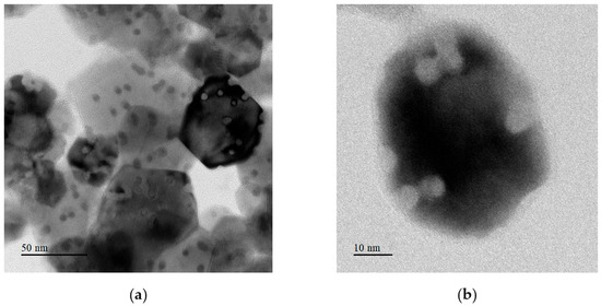
Figure 1.
BF TEM images of nc-Y2Ti2O7 irradiated with Kr ions at Se ≈ 15,8 keV/nm: (a) clusters of nanoparticles; (b) isolated nanoparticles.
With decreasing electronic energy loss, tracks are more efficiently produced in small, isolated crystals and in the border (thinner) regions of larger grains than in the interior (thick part) of larger grains, as shown in Figure 2 and Figure 3. The high-resolution image in Figure 2b clearly shows the lack of lattice fringes inside the track cores. Some random amorphous contrast variation is superimposed on the crystal due to the underlying amorphous carbon support film. Lattice fringes are still visible in the crystal, however. Figure 2c shows a dark-field image of the grain in Figure 2b taken with one of the strong lattice reflections. The bright contrast within the grain shows a crystalline region while the amorphous tracks remain dark. Hillock formation at the surface of a crystal leads to a zone of heavily damaged material below the hillock from where matter was expelled [15,16,17,18,19]. For small particles, this “near-surface” volume where damage is exaggerated may approach the entire thickness of the particle. This also explains the presence of amorphous tracks near the edges of larger particles near the free surface.
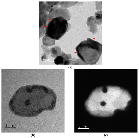
Figure 2.
TEM images of nc-Y2Ti2O7 irradiated with Bi ions at Se ≈ 7.5 keV/nm: (a) BF TEM image of clusters of nanoparticles showing amorphous tracks only at the edges, (b) BF TEM and (c) DF TEM images of isolated nanoparticles with amorphous tracks in the interior. Red arrows show defects at the cluster boundaries.
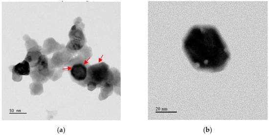
Figure 3.
BF TEM images of nc-Y2Ti2O7 irradiated with Xe ions at Se ≈ 3.9 keV/nm: (a) clusters of nanoparticles, (b) isolated nanoparticle with an amorphous track in the interior. Red arrows show small defects at the cluster boundaries.
TEM analysis of the irradiated crystals reveals some general features of track-associated radiation defects in nanosized yttrium titanate which are typical for other nanocrystalline dielectrics (see, for instance [22,31]) irradiated with SHIs. The smaller the size of the crystals and/or the thinner the crystals or their parts (located usually close to the crystal edge), the easier the incident ions produce tracks (Figure 2, Figure 3 and Figure 4).
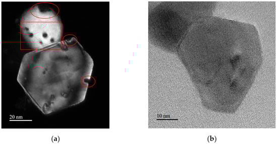
Figure 4.
TEM images of nc-Y2Ti2O7 irradiated with Xe ions at Se ≈ 7.9 keV/nm: (a) DF TEM; (b) HR TEM. Red circles show amorphous defects at the edges of crystals, and the red square shows amorphous tracks in the interior of a small particle.
Limited thermal transport out of isolated small particles may result in higher transiently attained temperatures after ion passage. This, together with surface related damage contributing a relatively large fraction of the total track damage in small particles, results in amorphous tracks forming in small, isolated particles, even at low electronic energy losses, where the observed structural defects in larger particles can no longer be considered as continuous amorphous tracks. Defects in larger particles are still visible in TEM due to the associated strain field of the defected region, as seen in the interior of the large grain in Figure 4a. These features are better described as discontinuous lines of defected crystal. High-resolution imaging shows that these defected regions remain crystalline in nature (Figure 4b). In this specific case, the crystal in question is about 35 nm by 45 nm in lateral dimensions and probably a similar thickness, which makes it a similar size to the one in Figure 2b. Both crystals were irradiated with ions of similar Se, although of different atomic species, yet the crystal in Figure 2b exhibits amorphous tracks as opposed to the crystalline tracks in Figure 4b. Presumably, the latter was impacted by ions with energies at the lower end of the range shown in Table 1 (and noting that the range of possible Se is larger than the mean deviation quoted). The general trend of the data is quite clear. At any given ion energy (and corresponding Se), on average, smaller particles exhibit larger tracks and smaller particles also (on average) tend to exhibit amorphous tracks at lower Se than larger ones. Energy deposition during ion passage is a stochastic process and specific energy loss may vary significantly at different positions along the ion trajectory. Smooth energy loss plots are a product of averaging many impacts and significant deviations from these averages are possible. Another trend that is clear from the data is that the border regions of particles (which are generally thinner in projection than near the middle of the particle) exhibit larger tracks and quite often show amorphous tracks at Se in the range where tracks near the centre are crystalline, as highlighted with circles in Figure 4a. Amorphous tracks in the interior of a small particle are highlighted by the red square. The results of TEM observation are summarized in Table 1 and presented in Figure 5 and Figure 6 as plots of ion track radii versus electronic energy losses for nanoclusters/large particles and isolated nanocrystals <50 nm in diameter. The “size” of discontinuous, strained crystalline tracks is not well defined and thus we restricted our analysis to amorphous tracks. When no amorphous tracks were detected, n/d is reported in the table. Tracks on the edge of particles, that are typically larger than tracks in the interior, were also excluded.

Table 1.
Ion irradiation parameters and track radii in nc-Y2Ti2O7.

Figure 5.
Dependence of the average radius of tracks, rb, on ionization energy losses, Se, in large crystals.
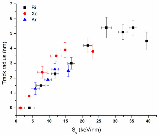
Figure 6.
Dependence of the average radius of tracks, rp, on ionization energy losses, Se in isolated nanoparticles below 50 nm diameter.
For isolated small nanoparticles, Table 1 shows that no amorphous tracks were detected when irradiated with Bi at Se = 4.0 ± 1.5 keV/nm but at 7.5 ± 1.3 keV/nm, tracks were detected. Similarly, for Xe irradiation, tracks were not detected at Se = 1.3 ± 0.7 keV/nm but were at 3.9 ± 1.2 keV/nm. For Kr irradiation, tracks were detected at the lowest Se of 5.8 ± 1.3 keV/nm.
For larger particles/clusters, we find that amorphous tracks were observed for Bi irradiation with Se = 16.7 ± 1.1 keV/nm but not for Se = 11.8 ± 1.1 keV/nm. For Xe, amorphous tracks were seen for Se = 12.1 ± 1.7 keV/nm but not for Se = 7.9 ± 1.5 keV/nm and for Kr, amorphous tracks were seen at Se = 11.7 ± 1.1 keV/nm but not at Se = 9.6 ± 1.1 keV/nm.
In all cases, the quoted uncertainty in Se is purely due to the energy dispersion induced by the Al degrader; initial ion bean energy dispersion was not considered. Furthermore, the quoted uncertainty is not the maximum deviation from the mean value but rather the mean of the absolute differences between the individual datapoints and the quoted mean. This means there may be ions with considerably higher energy (and lower) in the actual experiment and thus increased uncertainty in the real electronic energy loss for any observed track. For nuclear energy losses (Sn), only the mean value is quoted as Sn is typically only a small fraction of Se for SHI irradiation. Obviously, this statement does not hold for ions passing through thick degraders and losing most of their kinetic energy. There is a synergistic effect of Sn and Se resulting in a higher than expected sensitivity to ion track formation when significant Sn is involved [42,43]. This effect further increases the uncertainty in total energy loss for any given ion track observed and makes identification of precise Sth through observation of individual tracks impossible. From the data in Table 1 it is obvious that smaller isolated particles are, on average, more sensitive to track formation, but there is also a large spread in the actual particle sizes in which tracks were measured. We divided them into two bins of “isolated nanocrystals less than 50 nm in diameter” and “clusters of nanoparticles (more than 50 nm and agglomerated)” in order to demonstrate this increased sensitivity and concluded that, for smaller isolated particles <50 nm and >10 nm in diameter, Sth is between 3.9 ± 1.2 keV/nm and 1.3 ± 0.7 keV/nm. No amorphous tracks were observed for 4.0 ± 1.5 keV/nm but it should be emphasized that particle sizes varied significantly, and very small, isolated particles were quite rare, resulting in a high probability that sufficiently small particles were not sampled for this irradiation. For larger particles, tracks were observed at Se = 11.7 ± 1.1 keV/nm but not at 11.8 ± 1.1 keV/nm, indicating that the threshold should be within the interval 10.7–12.8 keV/nm, as highlighted in Figure 5.
It should be noted that, for 4 keV and 10 keV/nm, crystalline defects could be observed in clusters and large crystals and some amorphous defects could be found at the edges of larger crystals. At the lowest Se, amorphous defects were detected only in particles below ~30 nm in diameter (see, for instance, Figure 3b and Figure 4b).
To date, there are almost no published data on tracks in yttrium titanate except [22] and [32]. In [22], tracks were studied in polycrystalline Y2Ti2O7 irradiated with 2.2 GeV 197Au ions (Se = 35.7 ± 0.9 keV/nm) by XRD. Assuming that every ion produces an amorphous track and calculating the amorphous fraction as a function of ion fluence, the average track diameter was estimated as 4.6 ± 0.4 nm. This value is lower than that obtained for large and interconnected grains in this work at similar energy loss (d = 10.4 ± 0.8 nm). Strictly speaking, such direct comparison is not valid as different techniques with different limitations and sensitivities were used to examine the samples (TEM here and XRD in [22]) and the discrepancy might be related to non-uniformity of the track diameter along its length. A larger diameter near the surface (see Figure 4) would be dominant in TEM but much less obvious in XRD, where track uniformity is assumed.
Our results show that amorphous track formation in titanate pyrochlore is dependent on the size of target particles: the smaller the particle, the more sensitive it is to track formation (isolated nanoparticles > nanoclusters > polycrystals). As follows from Figure 5 and Figure 6, track radii tend to saturate and even decrease at high electron stopping powers. The “saturation” and decrease of the track size is the consequence of the effect of the ion velocity [44]. Track size is roughly an interplay of two factors: ion Se and the efficiency of energy transfer to the lattice. For low-velocity ions (below the Bragg peak) the ion Se increases with velocity. On the other hand, the efficiency of energy transfer decreases with velocity. This stems from the spectrum of generated electrons: the higher the velocity of an ion, the higher the maximum energies of the delta electrons produced by it. Faster electrons bring more energy out of the ion track, resulting in lower energy transfer to the lattice and thus a lower temperature inside it (lower efficiency of energy transfer). At low velocities the Se factor dominates, but at some energies the second factor becomes more important, leading to the saturation and eventual decrease of the track size.
3.2. MD Simulations of SHIs in Bulk and Nanosized Y2Ti2O7
Figure 7 shows an MD supercell of Y2Ti2O7 containing a 156 MeV Xe ion track, which manifests as an amorphous cylindrical region surrounded by a crystalline shell (Figure 7a). Analysis of the damage in the sublattices shows that amorphization occurred in the metal (Figure 7b) and oxygen (Figure 7c) sublattices, whereas a distorted shell developed mainly on the O sublattice. The diameter of the amorphous core is ~7.7 nm and the thickness of the shell ~1.2 nm (total diameter is ~10.1 nm).
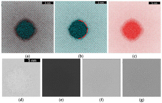
Figure 7.
(a) Simulated 156 MeV Xe ion track in YTiO; (b) metal sublattice (Y + Ti); (c) oxygen sublattice. Y/Ti/O atoms are shown as black/cyan/red dots. Dashed red line shows the borders of the amorphous part. Simulated TEM images with detector collection angle of (d) 0–5, (e) 5–10, (f) 10–15, (g) 15–25 mrad.
Annular bright-field (ABF) STEM images simulated from MD (Figure 7a) with 25 mrad convergence angle and detector collection angles of 0–5 mrad, 5–10 mrad, 10–15 mrad and 15–25 mrad, respectively, are shown in Figure 7d–g. The amorphous core is obvious on all simulated micrographs while the shell is not readily visible, even when using ABF STEM, which is sensitive to light atoms such as oxygen. Since the amorphous core is easily visible in TEM, we consider the amorphous region to be the effective track for the remainder of this paper.
In order to determine the threshold energy loss for track formation in bulk Y2Ti2O7, a series of MC+MD simulations were performed for ions of various masses and energies (low-velocity ions). The plot of calculated track radii vs. ion electronic energy loss is shown in Figure 8 together with the data from Figure 5. Ion tracks are not observed for Se ≤ 7.7 keV/nm (data point of Ar ion) while the lowest calculated track size was obtained for Se = 8.6 keV/nm. This allows us to estimate the threshold of track formation of 7.7 ≤ Sth < 8.6 keV/nm in bulk samples, which is below that estimated from Table 1.
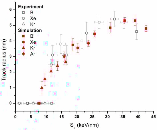
Figure 8.
Dependence of SHI track sizes on electronic energy loss of ions. MD results are compared with TEM results shown in Figure 5.
Figure 9 shows the results of simulation of Ar ion impacts in 20 nm spherical free-standing nanocrystals at 5.4 and 7.7 keV/nm forming tracks of hourglass shape. These tracks have the smallest diameter (~2 nm for 5.4 keV/nm and 4 nm for 7.7 keV/nm) in the middle part of the nanocluster expanding in the sub-surface regions. At 4 keV/nm energy loss, there appears only a distortion of the near-surface regions of ~3–4 nm depth. The presence of a free surface allows for expulsion of molten/disordered matter, resulting in a deficiency of material in the subsurface layers. The atoms in near-surface layers also have higher energies compared to the bulk, resulting in a lower threshold energy (or temperature) required to produce disorder. Due to these factors, and similarly to the situation in thin films [36], isolated nanoparticles demonstrate higher sensitivity to SHI irradiation, showing a lower track formation threshold [37].
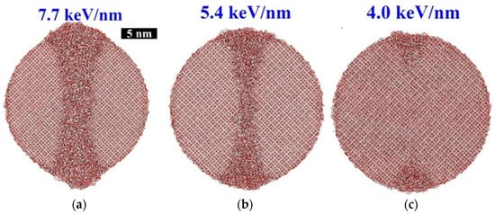

Figure 9.
MD snapshots of (a) 50 MeV Ar, (b) 10 MeV Ar and (c) 10 MeV Si ions in 20 nm spherical nanoclusters of Y2Ti2O7. Projections of 2 nm slices are shown. (a’,b’,c’) are corresponding perspective views with atoms coloured according to their displacements from the initial positions.
The calculation of SHI track formation in a larger (35 nm) spherical nanocluster is illustrated in Figure 10. An ion impact at Se = 5.4 keV/nm leads to slight damage of the surface region (3–4 nm depth). The remaining volume is basically undamaged, apart from a small lattice distortion visible as a slight colour change in Figure 10b. This allows us to conclude that the track morphology and energy loss threshold for track formation are strongly dependent on the size of the particles.
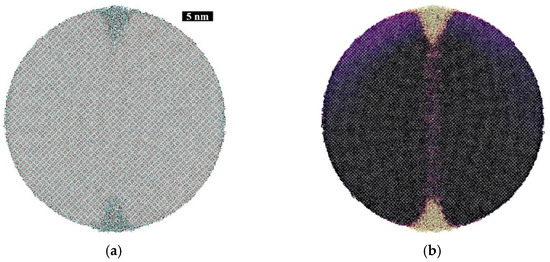
Figure 10.
(a) MD snapshot of 10 MeV Ar (5.4 keV/nm) in 35 nm spherical nanocluster of YTiO. Projection of 2 nm slices are shown. (b) Is corresponding view with atoms coloured according to their displacements from their initial positions.
4. Conclusions
Two types of particles were considered: isolated nanocrystals (<50 nm in diameter) and larger crystals typically forming part of polycrystalline conglomerates and usually above 100 nm in size. TEM data allow us to conclude that the particle size affects the size and nature of SHI-induced defects. Isolated nanoparticles were found to be the most sensitive to the SHI irradiation, with increasing susceptibility to track formation with decreasing size. The threshold electronic energy loss for the formation of amorphous tracks was estimated as 2.7–5.1 keV/nm for isolated nanocrystals below 50 nm in diameter. A value between 10.7 and 12.8 keV/nm was estimated for larger nanocrystals forming part of agglomerates. This value is slightly higher than reported for particles in a steel matrix [9] but still within the limits of uncertainty and should approach that of bulk Y2Ti2O7. Crystalline defects in nanoclusters are produced at 4 keV/nm < Se < 10 keV/nm. MD results highlight the influence of the free surface on the local track diameter. The two quoted Sth intervals for the two classes of particles studied should not be considered as precise values. Indeed, it would be impossible to quote a fixed value for a distribution of particle sizes since, clearly, Sth is particle size dependent. Still, more work is needed to understand how Sth varies with particle size and such future investigations would require a much narrower particle size distribution.
Author Contributions
Conceptualization, A.I. and J.O.; methodology, A.M. and R.R.; software, R.R.; validation, A.I. and J.O.; formal analysis, A.I. and J.O.; investigation, A.I., J.O., A.M. and R.R.; resources, J.O. and V.S; data curation, A.I. and J.O.; writing—original draft preparation, A.I. and J.O.; writing—review and editing, A.I., J.O., R.R. and V.S.; visualization, A.I. and R.R.; supervision, A.I., J.O. and V.S.; project administration, A.I.; funding acquisition, A.I., J.O. and V.S. All authors have read and agreed to the published version of the manuscript.
Funding
This research was funded by the Ministry of Education and Science of the Republic of Kazakhstan (grant number AP09058081) and the National Research Foundation of South Africa (grant number 70724).
Data Availability Statement
The data presented in this study are available on request from the corresponding author. The data are not publicly available due to funding requirements.
Acknowledgments
The authors thank L. Alekseeva for the synthesis of nanocrystalline yttrium titanate powder. Also, the authors are grateful to the IC-100, U-400 and DC-60 accelerator staff of the Flerov Laboratory of Nuclear Research, Joint Institute for Nuclear Research and Institute of Nuclear Physics.
Conflicts of Interest
The authors declare no conflict of interest.
References
- Moll, S.; Sattonnay, G.; Thomé, L.; Jagielski, J.; Legros, C.; Monnet, I. Swift heavy ion irradiation of pyrochlore oxides: Electronic energy loss threshold for latent track formation. Nucl. Instrum. Methods Phys. Res. Sect. B 2010, 26, 2933–2936. [Google Scholar] [CrossRef]
- Ewing, R.C.; Weber, W.J.; Lian, J. Nuclear waste disposal—Pyrochlore (A2B2O7): Nuclear waste form for the immobilization of plutonium and “minor” actinides. J. Appl. Phys. 2004, 95, 5949–5971. [Google Scholar] [CrossRef]
- Wang, S.X.; Begg, B.D.; Wang, L.M.; Ewing, R.C.; Weber, W.J.; Kutty, K.V.G. Radiation stability of gadolinium zirconate: A waste form for plutonium disposition. J. Mater. Res. 1999, 14, 4470–4473. [Google Scholar] [CrossRef]
- Wang, S.X.; Wang, L.M.; Ewing, R.C.; Was, G.S.; Lumpkin, G.R. Ion irradiation-induced phase transformation of pyrochlore and zirconolite. Nucl. Instrum. Methods Phys. Res. Sect. B 1999, 148, 704–709. [Google Scholar] [CrossRef]
- Lian, J.; Wang, L.M.; Wang, S.X.; Chen, J.; Boatner, L.A.; Ewing, R.C. Nanoscale manipulation of pyrochlore: New nanocomposite ionic conductors. Phys. Rev. Lett. 2001, 87, 145901. [Google Scholar] [CrossRef]
- Begg, B.D.; Hess, N.J.; McCready, D.E.; Thevuthasan, S.; Weber, W.J. Heavy-ion irradiation effects in Gd2(Ti2−xZrx)O7 pyrochlores. J. Nucl. Mater. 2001, 289, 188–193. [Google Scholar] [CrossRef]
- Lian, J.; Zu, X.T.; Kutty, K.V.G.; Chen, J.; Wang, L.M.; Ewing, R.C. Ion-irradiation-induced amorphization of La2Zr2O7 pyrochlore. Phys. Rev. B 2002, 66, 054108. [Google Scholar] [CrossRef]
- Lian, J.; Wang, L.; Chen, J.; Sun, K.; Ewing, R.C.; Matt Farmer, J.; Boatner, L.A. The order—Disorder transition in ion-irradiated pyrochlore. Acta Mater. 2003, 51, 1493–1502. [Google Scholar] [CrossRef]
- Skuratov, V.A.; Sohatsky, A.S.; O’Connell, J.H.; Kornieieva, K.; Nikitina, A.A.; Neethling, J.H.; Ageev, V.S. Swift heavy ion tracks in Y2Ti2O7 nanoparticles in EP450 ODS steel. J. Nucl. Mater. 2015, 456, 111–114. [Google Scholar] [CrossRef]
- Cureton, W.F.; Palomares, R.I.; Walters, J.; Tracy, C.L.; Chen, C.-H.; Ewing, R.C.; Baldinozzi, G.; Lian, J.; Trautmann, C.; Lang, M. Grain size effects on irradiated CeO2, ThO2, and UO2. Acta Mater. 2018, 160, 47–56. [Google Scholar] [CrossRef]
- Shen, T.D.; Feng, S.; Tang, M.; Valdez, J.A.; Wang, Y.; Sickafus, K.E. Enhanced radiation tolerance in nanocrystalline MgGa2O4. Appl. Phys. Lett. 2007, 90, 263115. [Google Scholar] [CrossRef]
- Zhang, J.; Lian, J.; Fuentes, A.F.; Zhang, F.; Lang, M.; Lu, F.; Ewing, R.C. Enhanced radiation resistance of nanocrystalline pyrochlore Gd2(Ti0.65Zr0.35)2O7. Appl. Phys. Lett. 2009, 94, 243110. [Google Scholar] [CrossRef]
- Nita, N.; Schaeublin, R.; Victoria, M. Impact of irradiation on the microstructure of nanocrystalline materials. J. Nucl. Mater. 2004, 329–333, 953–957. [Google Scholar] [CrossRef]
- Liu, W.; Ji, Y.; Tan, P.; Zang, H.; He, C.; Yun, D.; Zhang, C.; Yang, Z. Irradiation induced microstructure evolution in nanostructured materials: A review. Materials 2016, 9, 105. [Google Scholar] [CrossRef]
- Ishikawa, N.; Taguchi, T.; Ogawa, H. Comprehensive understanding of hillocks and ion tracks in ceramics irradiated with swift heavy ions. Quantum Beam Sci. 2020, 4, 43. [Google Scholar] [CrossRef]
- O’Connell, J.; Skuratov, V.; Janse van Vuuren, A.; Saifulin, M.; Akilbekov, A. Near surface latent track morphology of SHI irradiated TiO2. Phys. Status Solidi (b) 2016, 253, 2144–2149. [Google Scholar] [CrossRef]
- Ishikawa, N.; Taguchi, T.; Okubo, N. Hillocks created for amorphizable and non-amorphizable ceramics irradiated with swift heavy ions: TEM study. Nanotechnology. 2017, 28, 445708. [Google Scholar] [CrossRef]
- Zhai, P.; Nan, S.; Xu, L.; Li, W.; Li, Z.; Hu, P.; Zeng, J.; Zhang, S.; Sun, Y.; Liu, J. Fine structure of swift heavy ion track in rutile TiO2. Nucl. Instrum.Methods Phys. Res. Sect. B 2019, 457, 72–79. [Google Scholar] [CrossRef]
- Ishikawa, N.; Okubo, N.; Taguchi, T. Experimental evidence of crystalline hillocks created by irradiation of CeO2 with swift heavy ions: TEM study. Nanotechnology 2015, 26, 355701. [Google Scholar] [CrossRef]
- Allen, T.R.; Gan, J.; Cole, J.I.; Miller, M.K.; Busby, J.T.; Shutthanandan, S.; Thevuthasan, S. Radiation response of a 9 chromium oxide dispersion strengthened steel to heavy ion irradiation. J. Nucl. Mater. 2008, 375, 26–37. [Google Scholar] [CrossRef]
- Lescoat, M.L.; Monnet, I.; Ribis, J.; Dubuisson, P.; De Carlan, Y.; Costantini, J.M.; Malaplate, J. Amorphization of oxides in ODS materials under low and high energy ion irradiations. J. Nucl. Mater. 2011, 417, 266–269. [Google Scholar] [CrossRef]
- Shamblin, J.; Tracy, C.L.; Ewing, R.C.; Zhang, F.; Li, W.; Trautmann, C.; Lang, M. Structural response of titanate pyrochlores to swift heavy ion irradiation. Acta Mater. 2016, 117, 207–215. [Google Scholar] [CrossRef]
- Sellami, N.; Sattonnay, G.; Grygiel, C.; Monnet, I.; Debelle, A.; Legros, C.; Menut, D.; Miro, S.; Simon, P.; Bechade, J.L.; et al. Modifications of structural and physical properties induced by swift heavy ions in Gd2Ti2O7 and Y2Ti2O7 pyrochlores. Nucl. Instrum. Methods Phys. Res. Sect. B 2015, 365, 371–375. [Google Scholar] [CrossRef]
- Soulié, A.; Menut, D.; Crocombette, J.P.; Chartier, A.; Sellami, N.; Sattonnay, G.; Béchade, J.L. X-ray diffraction study of the Y2Ti2O7 pyrochlore disordering sequence under irradiation. J. Nucl. Mater. 2016, 480, 314–322. [Google Scholar] [CrossRef]
- Kishimoto, H.; Yutani, K.; Kasada, R.; Hashitomi, O.; Kimura, A. Heavy-ion irradiation effects on the morphology of complex oxide particles in oxide dispersion strengthened ferritic steels. J. Nucl. Mater. 2007, 367, 179–184. [Google Scholar] [CrossRef]
- Rogozhkin, S.V.; Bogachev, A.A.; Nikitin, A.A.; Vasiliev, A.L.; Presnyakov, M.Y.; Tomut, M.; Trautmann, C. TEM analysis of radiation effects in ODS steels induced by swift heavy ions. Nucl. Instrum. Methods Phys. Res. Sect. B 2021, 486, 1–10. [Google Scholar] [CrossRef]
- Trachenko, K. Understanding resistance to amorphization by radiation damage. J. Phys. Condens. Matter. 2004, 16, R1491–R1515. [Google Scholar] [CrossRef]
- Begg, B.D.; Hess, N.J.; Weber, W.J.; Devanathan, R.; Icenhower, J.P.; Thevuthasan, S.; McGrail, B.P. Heavy-ion irradiation effects on structures and acid dissolution of pyrochlores. J. Nucl. Mater. 2001, 288, 208–216. [Google Scholar] [CrossRef]
- Sattonnay, G.; Moll, S.; Thomé, L.; Legros, C.; Herbst-Ghysel, M.; Garrido, F.; Costantini, J.-M.; Trautmann, C. Heavy-ion irradiation of pyrochlore oxides: Comparison between low and high energy regimes. Nucl. Instrum. Methods Phys. Res. Sect. B 2008, 266, 3043–3047. [Google Scholar] [CrossRef]
- Skuratov, V.A.; Sohatsky, A.S.; O’Connell, J.H.; Kornieieva, K.; Nikitina, A.A.; Neethling, J.H.; Ageev, V.S.; Zdorovets, M.; Volkov, A.D. Stability of Y-Ti-O nanoparticles in ODS alloys during heat treatment and high temperature swift heavy ion irradiation. Physica status solidi (c) 2016, 13, 927–931. [Google Scholar] [CrossRef]
- Monnet, I.; Grygiel, C.; Lescoat, M.L.; Ribis, J. Amorphization of oxides in ODS steels/materials by electronic stopping power. J. Nucl. Mater. 2012, 424, 12–16. [Google Scholar] [CrossRef]
- Ibrayeva, A.; Mutali, A.; O’Connell, J.; Sohatsky, A.; Skuratov, V.; Alekseeva, L.; Korneeva, E.; Rymzhanov, R. Evaluation of threshold conditions for latent track formation in nanocrystalline Y2Ti2O7. Eurasian J. Phys. Funct. Mater. 2022, 6, 124–131. [Google Scholar] [CrossRef]
- Rane, A.V.; Kanny, K.; Abitha, V.K.; Thomas, S. Methods for synthesis of nanoparticles and fabrication of nanocomposites. In Synthesis of Inorganic Nanomaterials; Woodhead Publishing: Sawston, UK, 2018; pp. 121–139. [Google Scholar] [CrossRef]
- Lee, W.J.; Bae, D.S. Synthesis and characterization of Y2Ti2O7 photocatalytic powders by thermal assist process. Defect Diffus. Forum 2017, 380, 86–91. [Google Scholar] [CrossRef]
- Medvedev, N.A.; Rymzhanov, R.A.; Volkov, A.E. Time-resolved electron kinetics in swift heavy ion irradiated solids. J. Phys. D Appl. Phys. 2015, 48, 355303. [Google Scholar] [CrossRef]
- Rymzhanov, R.A.; Medvedev, N.A.; Volkov, A.E. Damage kinetics induced by swift heavy ion impacts onto films of different thicknesses. Appl. Surf. Sci. 2021, 566, 150640. [Google Scholar] [CrossRef]
- Rymzhanov, R.A.; O’Connell, J.H.; Janse van Vuuren, A.; Skuratov, V.A.; Medvedev, N.; Volkov, A.E. Insight into picosecond kinetics of insulator surface under ionizing radiation. J. Appl. Phys. 2020, 127, 015901. [Google Scholar] [CrossRef]
- Plimpton, S. Fast Parallel Algorithms for Short-Range Molecular Dynamics. J. Comput. Phys. 1995, 117, 1–19. [Google Scholar] [CrossRef]
- Dholakia, M.; Chandra, S.; Jaya, S.M. Properties of Y2TiO5 and Y2Ti2O7 crystals: Development of novel interatomic potentials. J. Alloys Compd. 2018, 739, 1037–1047. [Google Scholar] [CrossRef]
- Stukowski, A. Visualization and analysis of atomistic simulation data with OVITO–the Open Visualization Tool. Model. Simul. Mater. Sci. Eng. 2010, 18, 15012. [Google Scholar] [CrossRef]
- Berendsen, H.J.C.; Postma, J.P.M.; van Gunsteren, W.F.; DiNola, A.; Haak, J.R. Molecular dynamics with coupling to an external bath. J. Chem. Phys. 1984, 81, 3684–3690. [Google Scholar] [CrossRef]
- Jozwik-Biala, I.; Jagielski, J.; Arey, B.; Kovarik, L.; Sattonnay, G.; Debelle, A.; Mylonas, S.; Monnet, I.; Thomé, L. Effect of combined local variations in elastic and inelastic energy losses on the morphology of tracks in ion-irradiated materials. Acta Mater. 2013, 61, 4669–4675. [Google Scholar] [CrossRef]
- Jin, K.; Zhang, Y.; Weber, W.J. Synergistic effects of nuclear and electronic energy deposition on damage production in KTaO3. Mat. Res. Lett. 2018, 6, 531–536. [Google Scholar] [CrossRef]
- Toulemonde, M. Experimental phenomena and thermal spike model description of ion tracks in amorphisable inorganic insulators. Mat. Fys. Medd. 2006, 52, 263–292. [Google Scholar]
Disclaimer/Publisher’s Note: The statements, opinions and data contained in all publications are solely those of the individual author(s) and contributor(s) and not of MDPI and/or the editor(s). MDPI and/or the editor(s) disclaim responsibility for any injury to people or property resulting from any ideas, methods, instructions or products referred to in the content. |
© 2023 by the authors. Licensee MDPI, Basel, Switzerland. This article is an open access article distributed under the terms and conditions of the Creative Commons Attribution (CC BY) license (https://creativecommons.org/licenses/by/4.0/).