Article

Heterogeneity in La Distribution in Highly La-Doped SrTiO3 Crystals

by
Michał Marek Pilch
1,*,
Christian Rodenbücher
2,
Franciszek Krok
3 and
Kristof Szot
1,4
1
A. Chełkowski Institute of Physics, University of Silesia in Katowice, 75 Pułku Piechoty 1, 41-500 Chorzów, Poland
2
Forschungszentrum Jülich GmbH, Institute of Energy and Climate Research (IEK-14), 52425 Jülich, Germany
3
Marian Smoluchowski Institute of Physics, Faculty of Physics, Astronomy and Applied Computer Science, Jagiellonian University, Lojasiewicza 11, 30-348 Krakow, Poland
4
aixACCT Systems GmbH, 52068 Aachen, Germany
*
Author to whom correspondence should be addressed.
Crystals 2023, 13(11), 1552; https://doi.org/10.3390/cryst13111552
Submission received: 8 September 2023 / Revised: 15 October 2023 / Accepted: 25 October 2023 / Published: 30 October 2023

Abstract

:
Our paper is focused on the investigation of the dopant distribution in lanthanum-doped strontium titanate (LSTO) single crystals with a 5 wt.% doping level of La. Using X-ray diffraction analysis and pycnometric density measurement, we have found a discrepancy between the theoretical density and the experimentally determined value. The origin of this behavior could be either the creation of the voids in the matrix or the intergrowth of secondary phases with La surplus in the crystal. Transmission electron microscopy (TEM), energy-dispersive X-ray spectroscopy (EDX), and selected area diffraction (SAD) microscopic investigation have confirmed the second hypothesis, namely, that in different regions of LSTO, the local concentration of La shows a substantial variation on the micro- and nanoscopic scale. In order to study the influence of the La dopants on the electronic structure and, therefore, on the electrical conductivity, we have used the local conductivity atomic force microscopy (LCAFM) method as a local electrical probe to map the in-plane electrical conductivity of the La-doped crystal’s surface. The LCAFM conductivity maps reveal heterogeneous conductivity (here in the form of the bands with higher conductivity than the surroundings), related to band-like inhomogeneities of the La distribution. Using LCAFM measurements with atomic resolution obtained between the conducting and nonconducting regions, we analyzed the spreading (spatial expansion) of doping on the undoped or low-doped part of the STO crystal. The found limitation of the doping effect of La on the dielectric part of the STO crystal to 4–5 lattice constants was in good correlation with ab initio studies from the literature.

1. Introduction

The transformation of stoichiometric SrTiO3 crystal (as a band gap insulator) into a metallic conductor can be generated via self-doping (this corresponds to the generation of so-called delta non-stoichiometry, SrTiO3−x) or by donor doping on Sr or Ti atomic sites. In this way, doping with the aliovalent transition metal Nb was used to fabricate the most popular metallic substrate with perovskite structure, which, e.g., has broad applications for the thin-film deposition of multinary oxides. Although Nb-doped crystal growth was mastered as early as the late 1960s, the perfection of the crystal with high doping leaves much to be desired, and their real defect structure is still under discussion. Surprisingly, an analogous metallic SrTiO3 crystal with La donor substitution on Sr sites has not yet achieved the same technological development as its counterpart with Nb doping, although the ceramic LSTO has significant potential for photocatalysis, hydrogen production, water splitting [1,2], thermoelectric, and SOFC applications [3]. In this paper, we focus our research on the inhomogeneity distribution of the La dopant atoms in doped STO epipolished or cleaved crystals. The crystals were obtained via the Verneuil method, cut in the appropriate orientation, and epipolished. The crystals were purchased from CrysTEC, GmbH, Berlin, Germany. Following the statistical distribution of the La dopant in the SrTiO3 matrix, we already detected a problem from X-ray tests. The results of interdisciplinary research to determine the variance and homogeneity of the distribution of La cations in the LSTO matrix will be presented. In particular, we will emphasize the results of local electrical conductivity measurements by the LCAFM technique, which can be considered a method of choice for directly monitoring the La distribution at the micro- and nano-scale. In addition, based on electrical mapping data obtained with atomic resolution, we will describe the distribution of the electrical conductivity between regions of varying conductivity resulting from changes in the level of La doping. In this way, we will combine experimental data and theoretical calculations to understand the doping effect of the STO crystal matrix.

2. Point Defect Chemistry of La-Doped SrTiO3

To date, extensive point defect chemical studies on LSTO have shown that substituting Sr with 3+ La can occur in various ways [4,5,6]. On the one hand, in case of the preservation of the overall stoichiometry in the alkali metal sublattice (here Sr1−xLaxTiO3), the compensation mechanism of involving an additional electron contributed by La induces its transfer to the titanium ions. This process results in a shift in the valence of Ti from 4+ to 3+. In the context of electronic doping, the chemical formula for this alloy can be expressed as Sr1−xLaxTi4+1−xTi3+xO3. The crystal becomes a dark hue in color, in contrast to the typical lilac color associated with low levels of La doping. As in barium titanate, a “color change” is observed in La-doped strontium titanate at room temperature during the transition from electron-compensated (lilac in transmitted light) to metal-less compensated strontium titanate (crystal clear) [7]. Furthermore, this alteration leads to a shift in its electrical conductivity to the ‘n-type’ or metallic. On the other hand, it is possible to introduce La into the strontium titanate matrix without changing the ionization state of Ti and preserving its electrical neutrality, generating vacancies in the cationic subnetwork. The so-called vacancy compensation mechanism can be achieved through a reduction in the Sr concentration within the crystal, accomplished by simultaneous La doping of SrTiO3. In this case, the chemical formula can be represented as follows: Sr1−3/2x(VSr″)3/2x LaxTiO3, a phenomenon commonly referred to as ‘strontium vacancy compensation’. Still another vacancy compensation mechanism can be achieved if Ti vacancies are introduced in the TiO2 sub-lattice. The under-stoichiometry of Ti cations in LSTO (Sr1−xLaxTi1−x/4(VTi″″)x/4O3) helps compensate for the excess electrons introduced by La doping in the matrix. Importantly, for metal vacancy compensation, the doped SrTiO3 crystal remains transparent. A comprehensive analysis of point defects in La-doped SrTiO3, based mainly on the Brouwer diagram supporting these hypotheses, can be found in reference [5].
When discussing the nature of defects in LSTO, a fundamental question arises: what concentration of defects in the crystal cannot be analyzed in terms of a dilute solution? The interaction between charged point defects through long-range electrostatic forces must be considered for this critical concentration. Statistically distributed defects may be less favorable (from an energetic point of view) to defect accumulation in the form of one-, two-, or three-dimensional defects. In fact, it has been reported that, in the case of STO with a high dopant concentration with La, the formation of extended defects such as shear-plane, stacking faults, or other phases, e.g., LaTiO3 or R-P phases [5,8,9,10] can occur. Secondary ion mass spectrometry (SIMS) studies of in-plane La mapping in a monocrystal doped with 5% La revealed that the distribution of La is non-uniform and displays a band-like pattern [11]. Similarly, the spatial variation of the fluorescence time on the surface of the LSTO crystal is another indicator of the modulation of the semiconductor/metallic properties due to the inhomogeneity of La distribution mentioned above [11].

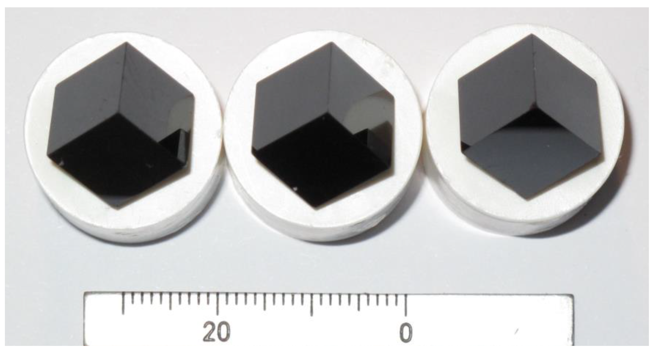
3. X-ray Diffraction Measurements and Density Determination

Already, X-ray studies and density measurements performed for highly doped STO crystals (here 5% La) shed light on the existence of inhomogeneities in La distribution in the crystal matrix. Despite the very good crystallographic quality and stoichiometry of the La-doped crystal used (see Figure 1 and Figure 2a–c), we observed that as the level of La doping gradually increases from 0.1% to 1% and 5%, the discrepancy between the theoretical density and the experimental density determined by the Archimedes method increases. It is important to highlight that, for the sake of precision in the density studies, we utilized crystals of substantial volume. Each doped crystal in our research possessed a cubic shape of 1 cm3 volume with epi-polished surfaces ({100}), as illustrated in Figure 1. A comparison of results between Archimedes density measurements and X-ray density is presented in Table 1. The comparison shows that the LSTO crystal with 0.1% La doping possesses the best density; the experimental density equals the theoretical (here X-ray) density. The further increase in the concentration of La in the matrix (to 1 and 5%) of our La-doped crystals leads to the progression of the density deviation (the Archimedes density shrinks to 98.9% for 5% La in STO). The XRD patterns obtained during our study consistently exhibit the characteristic perovskite structure, with a regular arrangement (Pm3m) across all doping levels, devoid of any foreign patterns. The lattice constants calculated from our XRD analysis are shown in Table 1.
In the first step, we analyzed the crystallographic structure and concentrated on determining the lattice parameters. The XRD measurements revealed that for all doping levels, the patterns were typical for perovskite with the regular system (Pm3m) without a foreign pattern. The lattice constants, which have been calculated from our XRD analysis, are presented in Table 1.
Analysis of the XRD data (see red curve in Figure 3) reveals that the lattice constant, 0.39054 nm, determined for the stoichiometric crystal, is close to the ideal value measured using the precise Bond method (a = 0.3905268 (98) nm [5]). However, already for 0.1% doping of La, our data showed a lattice collapse relative to the reference stoichiometric STO crystal.
The present finding of the LSTO lattice parameters dependence on La doping level stands in contrast to the X-ray measurements reported by Kobayashi, Ikuhara et al. [12] (blue curve in Figure 3). They observed a monotonic lattice expansion as the level of La doping in the STO matrix increased, and they explained this using the electronic compensation mechanism. On the contrary, similar to our 0.1% La-doped STO crystal, Moos et al. [4,5,6] observed a reduction in lattice constants for La-doped STO ceramics and explained it using a mechanism specifically in terms of “vacancy compensation”.
Our crystals, already with 0.1% La doping, changed their color to dark blue, indicating the existence of electronic compensation in the crystal. As expected, for electron compensation in a LSTO crystal, the lattice constant measured by the X-ray technique increased as the doping level increased (from 0.1% to 5%). This is in contrast to the XRD measurements obtained by Kobayashi, Ikuhara et al. [12] and Wang et al. [13] for LSTO with electronic compensation, which revealed a permanent expansion of the lattice with an increase in the doping level of La in the STO matrix only for the range of 0–0.1% La doping. A similar trend in the shrinking of the lattice parameters, as for our LSTO crystal doped with 0.1% La, was described by Moos et al. [4,5,6] for La-doped ceramics with vacancy compensation. Surprisingly, our dark blue crystal with 0.1% La doping (the observed change in the color and the increase in electrical conductivity should indicate the existence of electronic compensation in the crystal) possessed the best agreement between the XRD and Archimedes density. The increase in the concentration of La in the matrix to 1% and 5% led to the progression of the density deviation (the Archimedes density shrank to 98.9% for 5% La in STO). Additionally, an expected dependence between the dimension of the unit cell and doping level for electronically compensated LSTO crystals could be observed. Namely, the X-ray study confirmed that the lattice constant increased. On the one hand, we have a perfect single-crystalline X-ray pattern in our crystal, but on the other hand, the density of crystals with a high doping level shows a quality that is typical for good ceramics [14]. To explain the observed dramatic decrease in crystal density, we can consider two scenarios: either we have a poor-quality crystal with a high density of voids (in STO, this behavior was reported by Battle et al. and Wang et al. [9,13] and by Pilch or Rodenbücher from Prof. Szot’s group [15,16,17]) or the doping compensation mechanism has to be changed from electronic compensation to void compensation. Optical inspection did not show the existence of air bubbles, and the dramatic increase in electrical conductivity (shown in the next section) indicates the irrelevance of the presented scenarios. A third alternative, which questions the concepts of crystallographic structure with voids, may arise from studies of the layered structure of the La4Srn±4 TinO3n+2 family. X-ray diffraction data obtained for a member of this family for n ≥ 12 show a typical pattern for a cubic structure (Pm3m) with a lattice parameter similar to our X-ray data of 5% La (here 3.9065 Å), and in addition, the density of 5.26 g/cm3 is identical to our calculated theoretical density. This behavior can be analyzed in terms of the so-called intergrowth model, which shows that the perfect STO matrix is intergrown with the second phase of the La-reach structure. Unfortunately, the X-ray analysis and density analysis of the crystals we studied do not allow us to confirm which of the presented models is consistent with our experimental data. Nevertheless, these findings clearly show that the simple characterization of the La-doped STO crystal as a pristine perovskite is untenable. Therefore, we expanded our analysis to include a study using TEM methods.

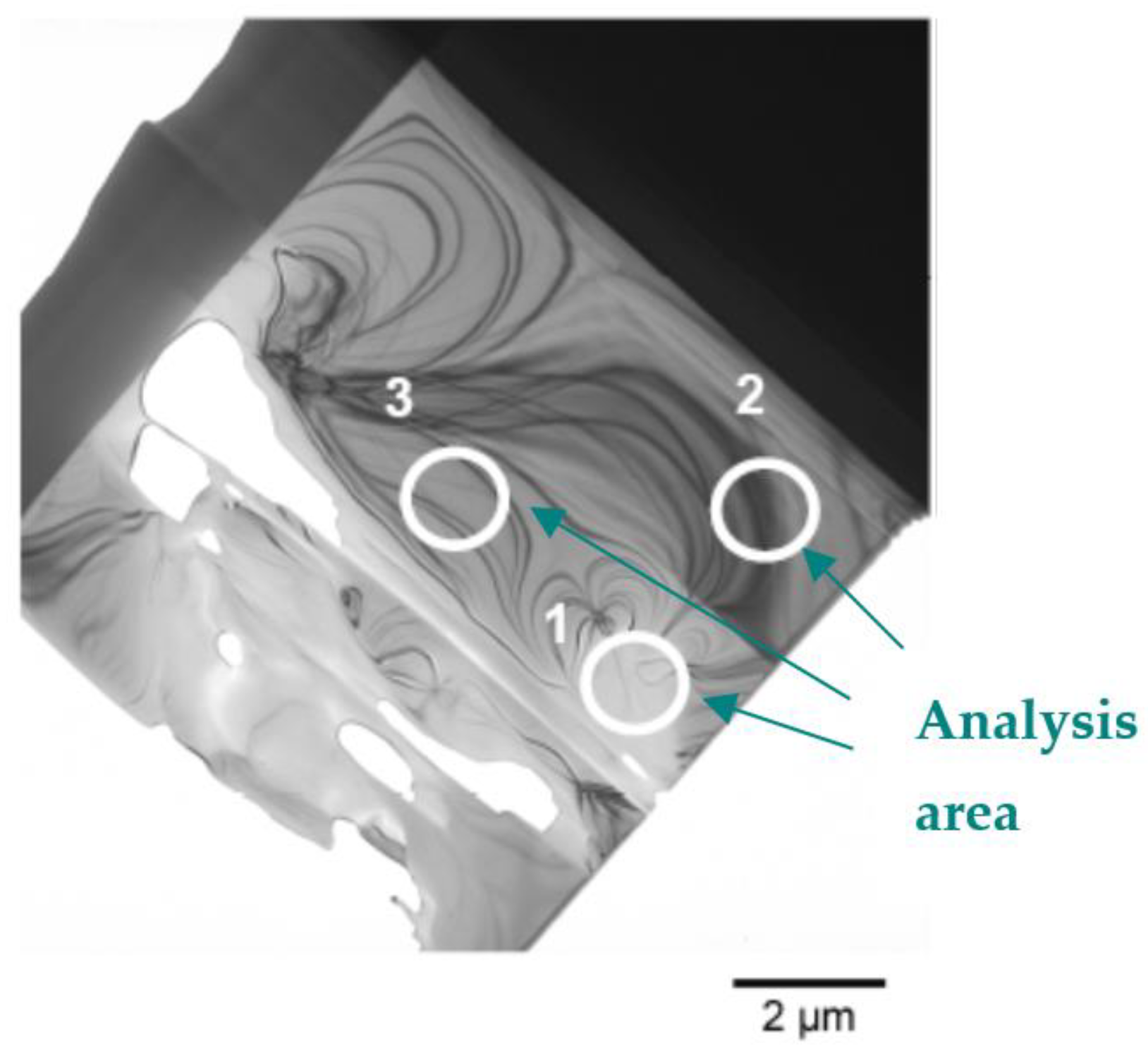
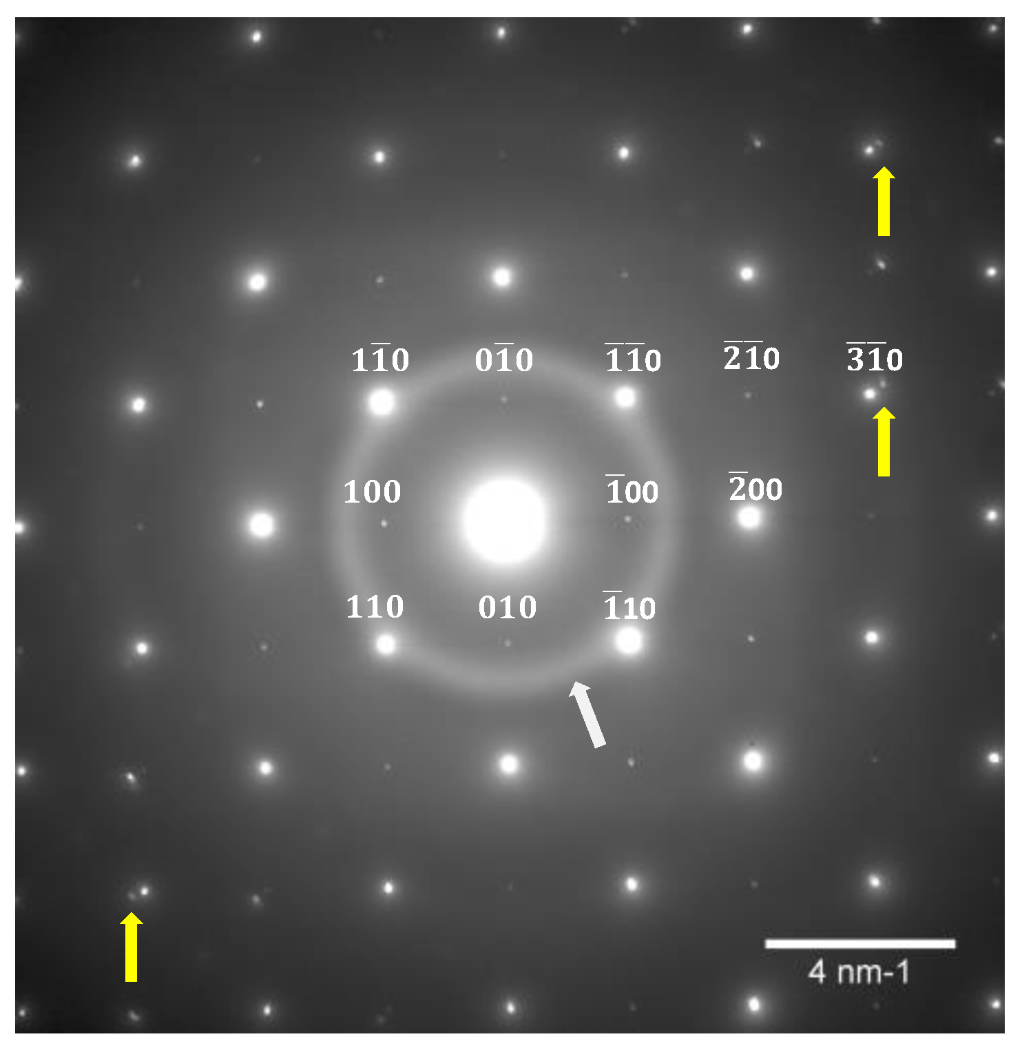
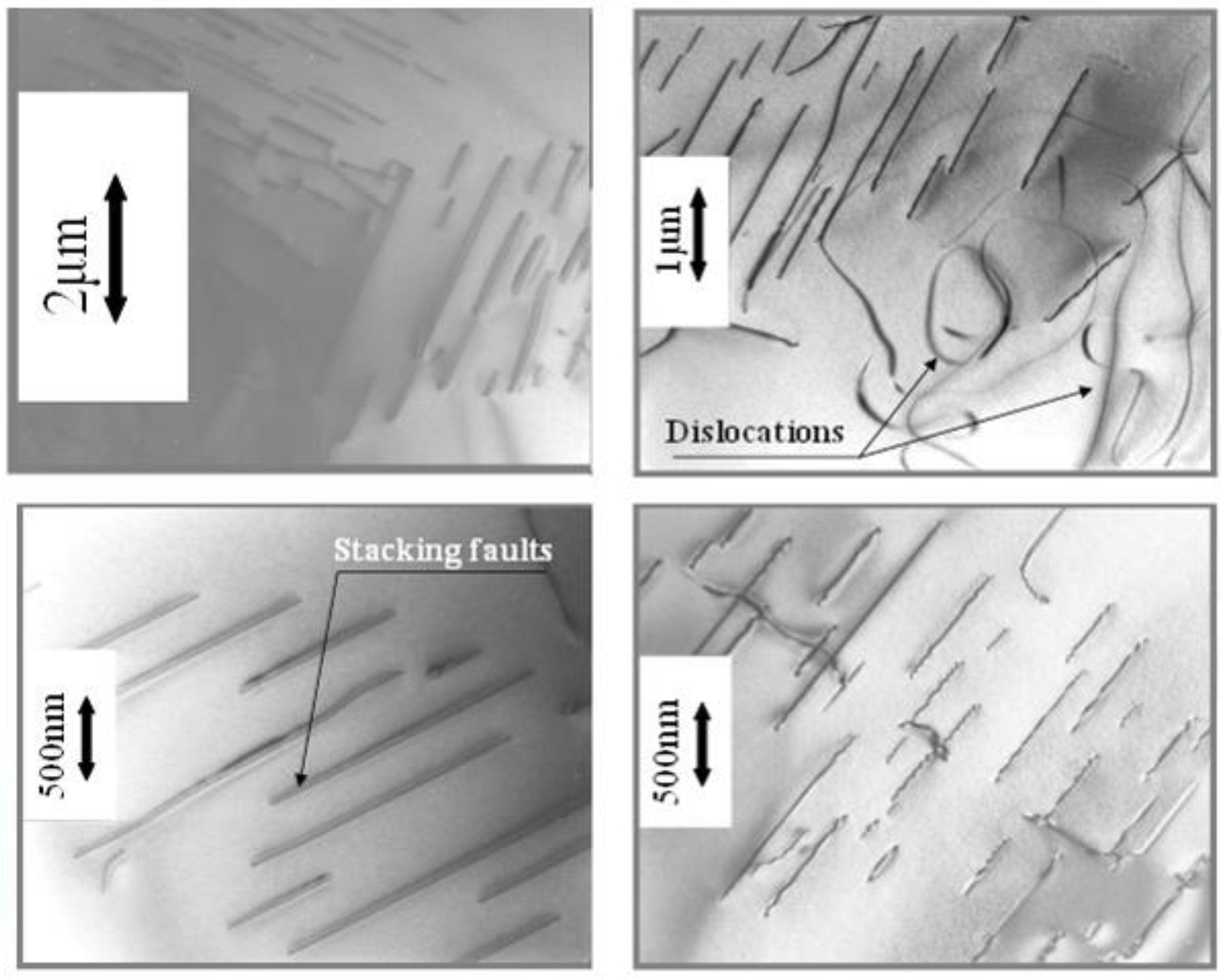
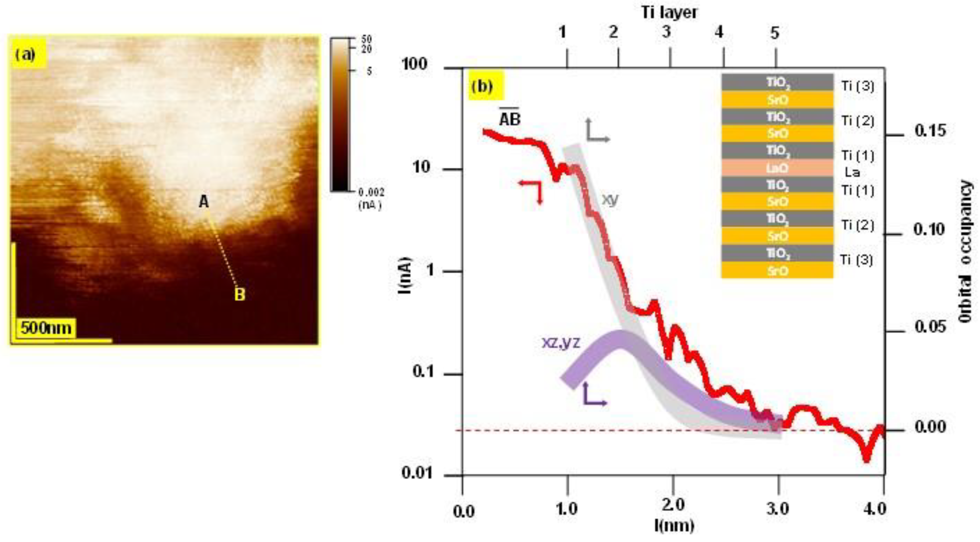
4. TEM, EELS, EDX, and SAD Analysis

Transmission electron microscopy (TEM)-based techniques enable the investigation of both the crystallographic structure and chemical composition of samples at the micro- to nanoscale range These microscopic studies were obtained on a thin lamella produced from the La-doped STO crystal by the Focus ion beam (FIB) process. In contrast to EDX measurements on bulk materials, the lateral resolution of the elements for thin foils is much better, so it was possible to check the exact concentration of Sr, Ti, and La doping cations on a small area of the lamella. EDX measurements on STO with a nominal 5% La doping, performed in three different areas on the lamella (Figure 4), showed significant variations in chemical composition (see Table 2).
According to EDX measurements, the La concentration in LSTO changed by 50% over a distance of a few micrometers. These results are in line with our previous SIMS studies, in which La distribution (in-plane of a polished surface crystal (100)) showed heterogeneous La doping in the form of bands, with the La enrichment in the center of the band [11]. A consequence of the relative change in the local concentration of dopant cations is a modification of the local electronic structure, which we observed in the electron energy loss spectroscopy (EELS) spectra (Figure 5). Namely, the amount of Ti in the valence 3+ charge state increased with the local La increases. This behavior indirectly confirmed that an additional electron introduced from doped La cations into STO led to electronic compensation, for which extra electrons were transferred to Ti. This finding agrees with our previous fluorescence lifetime study [18], revealing that the mentioned inhomogeneity in the doping of La leads to a variation of the local electronic structure.
The presented microscopic EDX inspection shown in Figure 6 of the significant variation in chemical composition at different locations of LSTO lamellae indicates that the local change in the La concentration cannot just be explained by a modification of the statistical level of doping in the context of classic Schottky disorder. Moreover, this can lead to defect formation of higher dimensionality than the point defect that can modify, e.g., the original crystallographic structure. Finally, a local change in doping levels, at least due to induced lattice expansion, can be expected to cause a change in the lattice constant. At first glance, the SAD diffraction pattern contradicts such an argument; despite this heterogeneous doping level, our structure appears to have a typical pattern for a cubic structure. However, a close analysis of the pattern identifies some deviations from the ideal structure characteristic of cubic systems: a doubling of the lattice constant with an additional reflection that can be attributed to the twisting of the region that was analyzed by SAD and the existence of the amorphous ring, which could indicate “partial crystallographic chaos” on the part of our doped LSTO crystal.
This observation is confirmed by high-resolution TEM measurements (see Figure 7). In fact, different kinds of linear and planar defects, such as dislocations and stacking faults, can be identified in TEM photography. These results align with the previously analyzed modifications of the lattice parameter and the unusual change in the real density of the crystal for a high doping level of La.

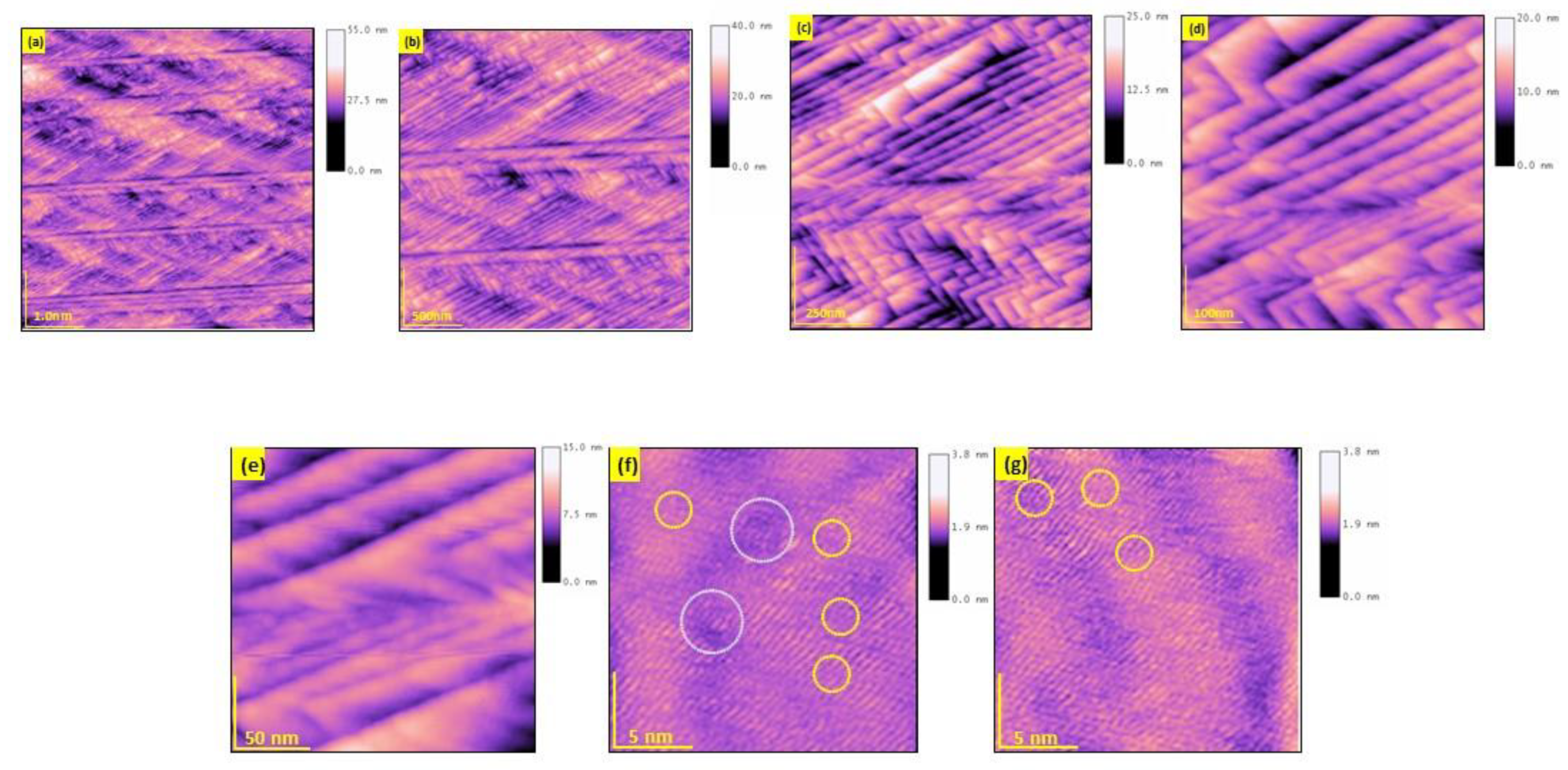
5. Optical Inspections and Morphological Analysis of Cleaved Plane

We have reported that for the high doping level of Nb in a STO crystal, the optical inspection of the thin crystal shows spatial modulation of the local transparency due to the inhomogeneous distribution of dopants [18]. It should be noted that Nb-doped crystals with reasonable homogeneous optical quality can rarely be found. We have obtained similar optical characterizations of La-doped crystals. Unfortunately, the thin crystal with 5% La (0.1 mm) had too low transparency; therefore, we investigated the thin STO crystals with 1% La doping (see Figure 8). Our optical examination revealed a band modulation of local transparency similar to that found in the uneven distribution of La using the SIMS analysis. Since inhomogeneous doping can affect the local mechanical properties, we tried to test the morphology of the crystal cleavage (parallel to the (001) plane). In contrast to the conical shape of the cleavage plane of undoped STO [19] in the case of 5%-doped La crystal, banded ordering of the micro-facets can be observed on such a prepared surface by AFM (see Figure 9a–e).
Atomically resolved AFM topography (Figure 9f,g) shows a high concentration of dislocations (marked by yellow circles). In regions depicted in the gray circle (Figure 9f), the atomic ordering is disturbed, which may explain the existence of an amorphous “halo” in the SAD pattern.

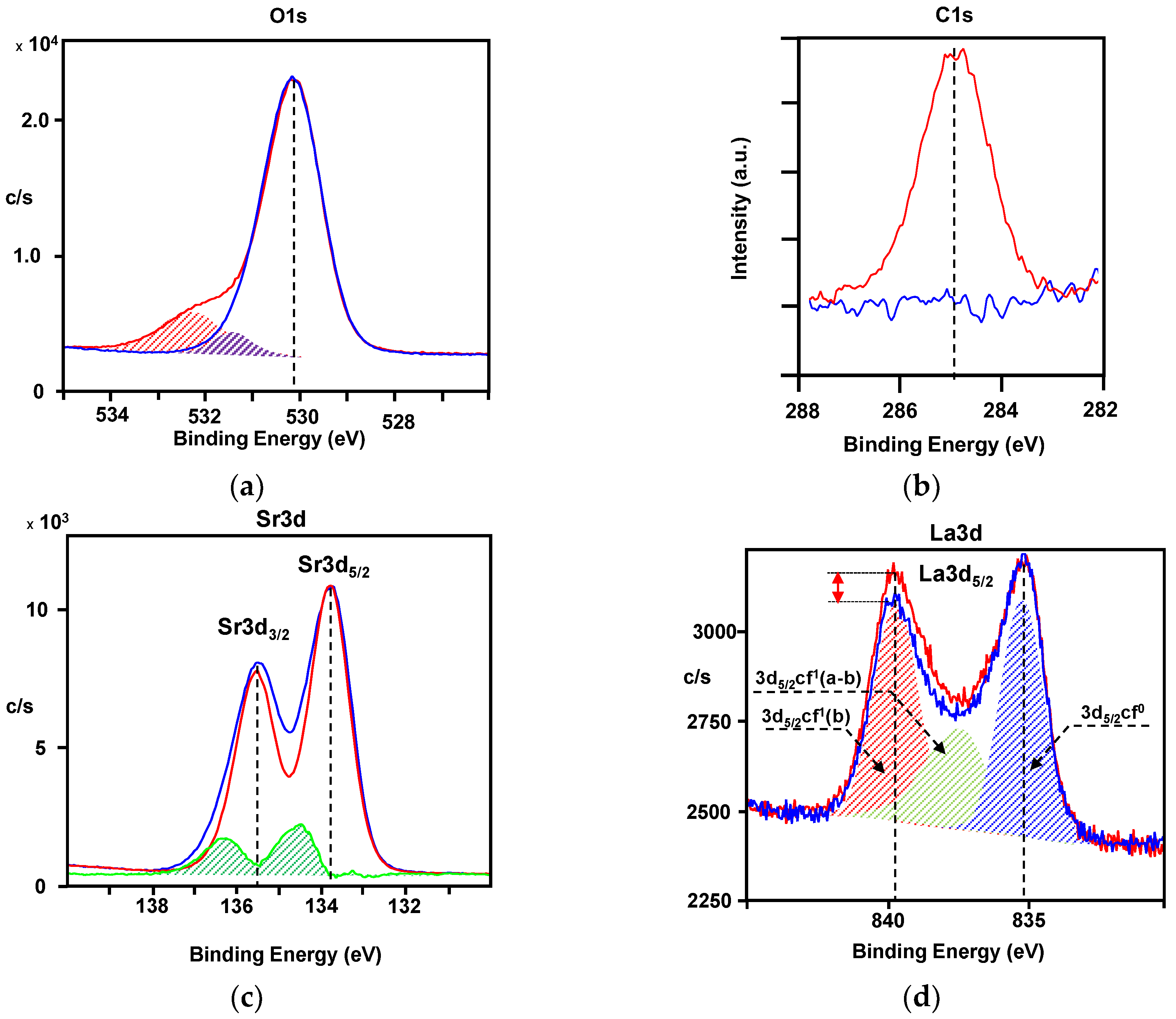
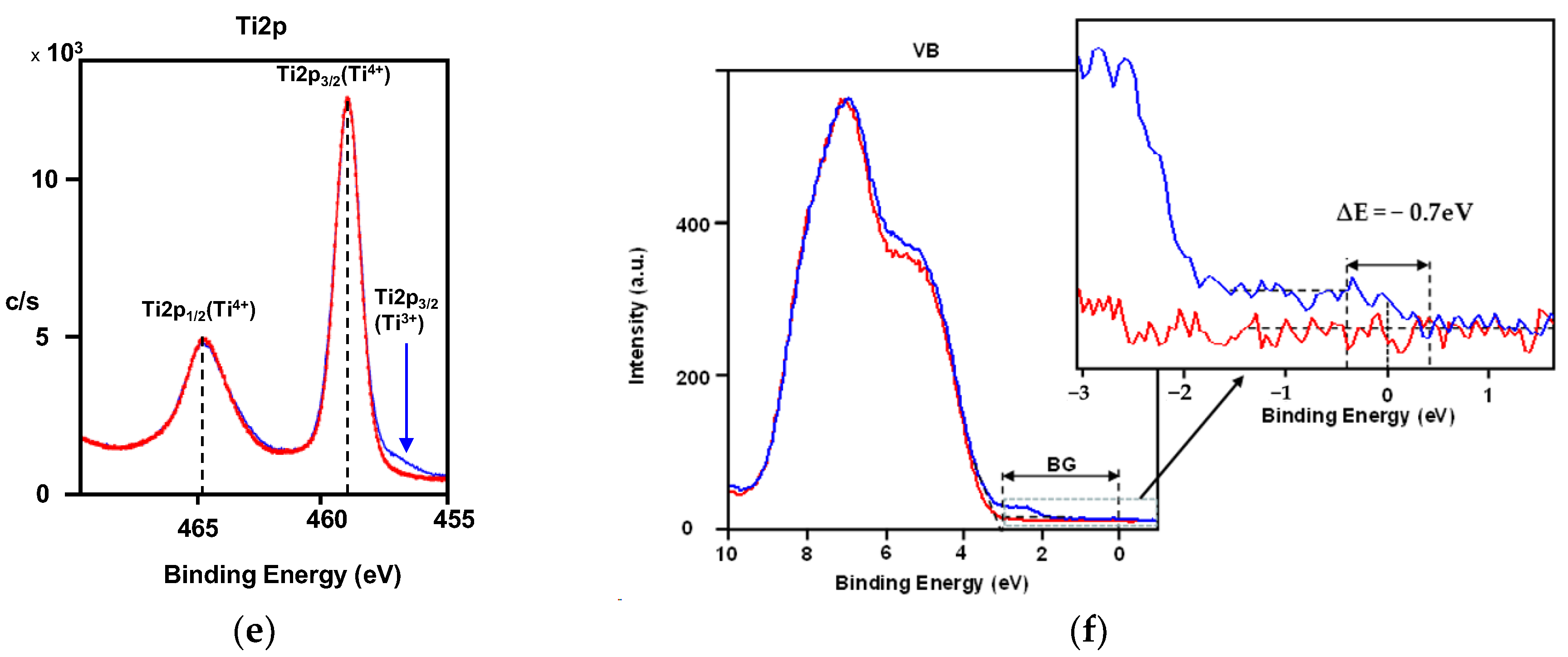
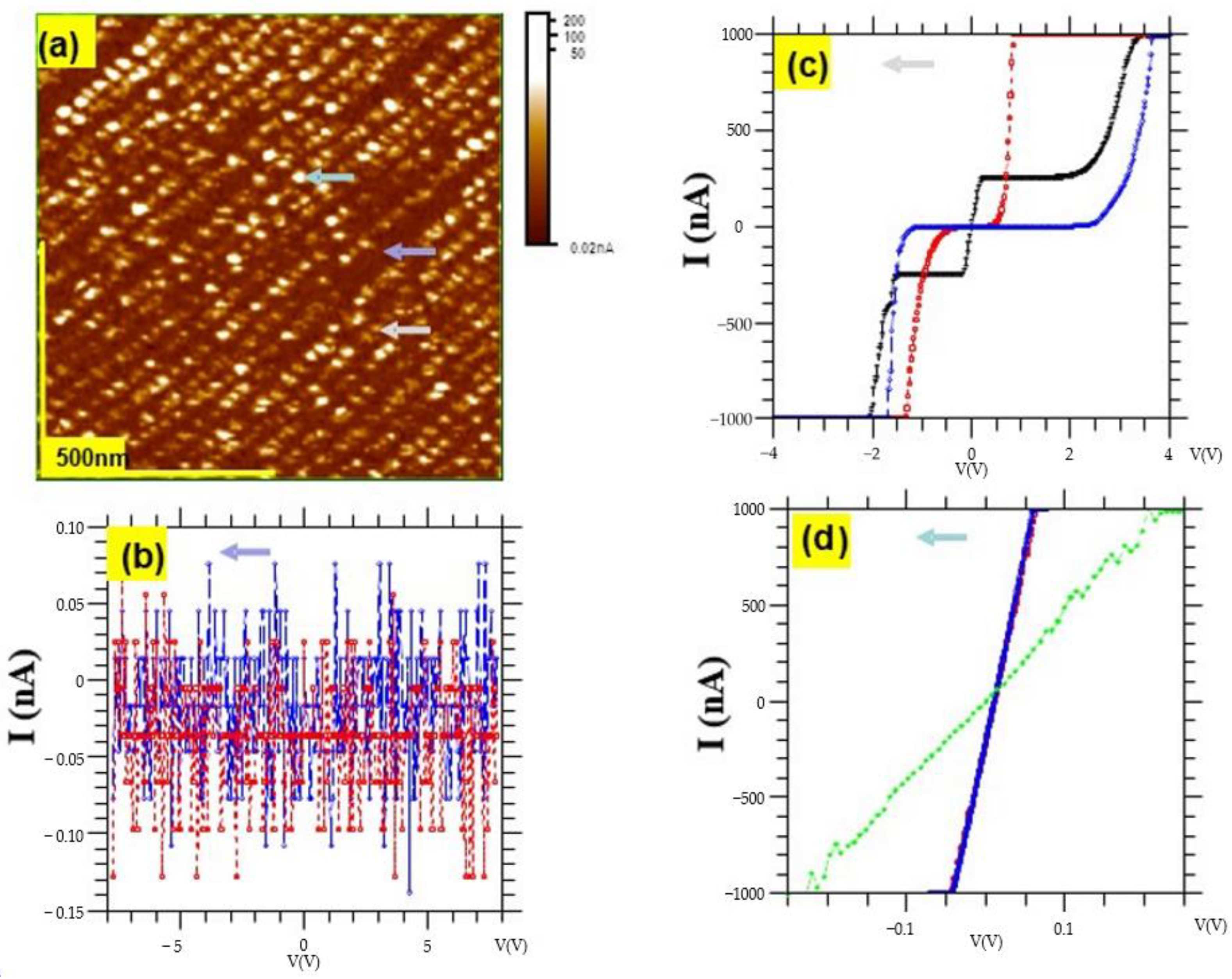
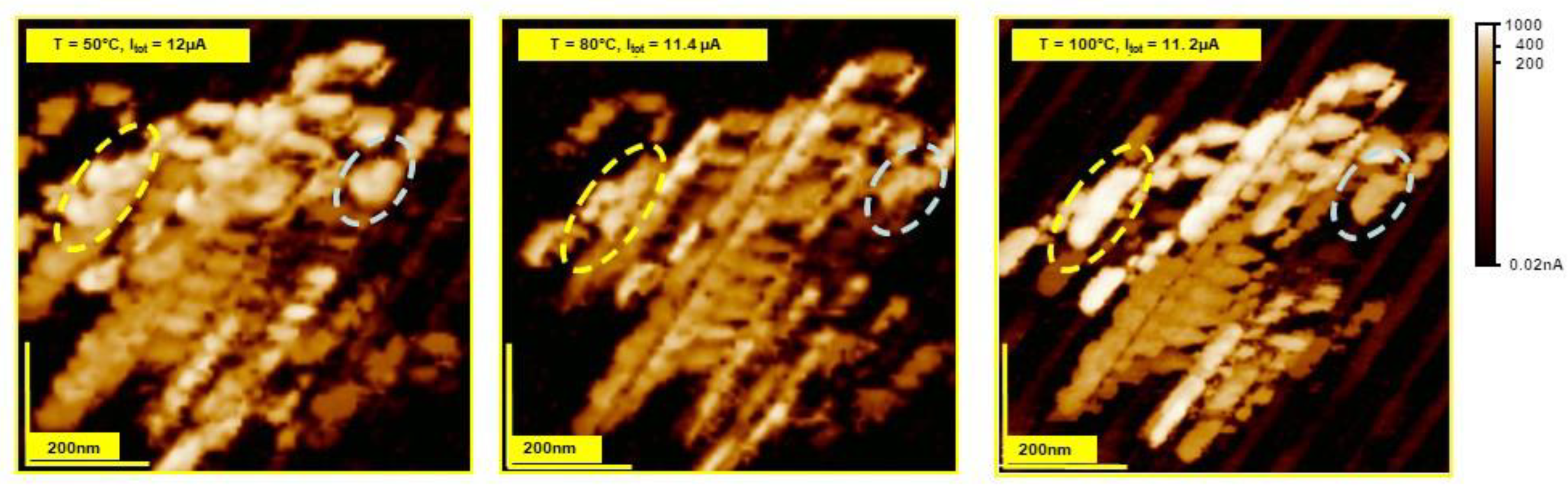
6. Surface-Sensitive Studies of the Electronic Structure and Electrical Conductivity on the Surface of LSTO; XPS and LCAFM Investigation

For electrical compensation, point defect chemistry predicts an increase in the electrical conductivity of La-doped STO with an I/M transition limit at La concentration levels between 0.1–1% La. An ex-situ LCAFM study of the cleaned, epi-polished LSTO surface was carried out to determine the level of electrical conductivity of doped STO and its surface distribution. We observed no surface conductivity in the case of LSTO with a 5% doping level unless a voltage exceeding −3 V was applied (Figure 10). However, when high polarization voltages were applied to the AFM tip, the surface topography exhibited significant changes consistent with the concept of ‘local chemical transformation at the surface,’ as described by Pellegrino et al. [20].
The lack of conductivity on the surface of the studied crystals was due to the presence of a layer of adsorbates. Analysis of the O1s and C1s XPS lines (Figure 11) showed that the LSTO surface was contaminated with water or hydroxyl groups, carbon oxides, and other carbon compounds (e.g., CHx). The concentrations of La in LSTO were obtained from XPS analysis of scrapped in-situ, as-received crystals. The chemical formula for scrapped in-situ crystals is Sr0.97La0.03TiO3 from calculation of the ratio Sr:La.
The chemistry of the contaminated surface layer leads to the formation of a sublayer with dielectric properties. As a result of leaching, the electronic structure of the crystal’s outermost monolayer may undergo modifications, causing the occupied state at the Fermi level, introduced into the system by La doping, to vanish (refer to the VB band gap with LSTO [2,21,22,23,24,25,26] as depicted in the blue curve in Figure 11). Therefore, one should remove this contaminated layer to determine the correlation of La distribution with the local electrical conductivity of LSTO using LCAFM. Scraping it off the crystal surface under ultra-high vacuum (UHV) conditions is a simple possibility. The effectivity of this preparation step can be derived from the XPS spectra (Figure 11; see the red spectra). Namely, in the O1s, any additional compounds typical for the chemical and physical sorbates exist. The disappearance of the C1s line from XPS spectra proves the surface is clean. This preparation step “revealed” the metallic properties of the LSTO surface crystal. Namely, the electronic states can be identified at the Fermi level near the bottom of the conduction band (see the blue spectrum of the VB regions in Figure 11).
Additionally, the Ti2p spectrum shows an appearance of the Ti3+ charge state at lower binding energy. It should be noted that the amount of Ti (of a lower charge state) is proportional to the concentration of La in the matrix; here, 5%. This finding directly proves that the studied doping with La has forced the electronic compensation in the STO crystal. Although the presented cleaning procedure demonstrated its effectiveness for unveiling metallic properties, we should notice that the SrO surface layer on fractured/scraped crystals showed an additional chemical state typical for SrO termination or stacking of SrO on SrO. In the La3d XPS core line, only small modifications of the bounding part of the compound La3d5/2 c1f1 are induced by mechanical preparation in situ.
Having a clean LSTO surface, LCAFM measurements reveal lateral non-uniform conductivity, characterized by high-conductivity regions contrasted with dielectric areas (Figure 12a). This behavior is in line with our EDX and SIMS [11] measurements, which have shown a spectacular modulation of the local doping level of La. The I/V characteristic obtained from the region of good conductivity (Figure 12c,d) showed distinct differences from the regions with a low level of La doping (Figure 12b). The regions of increased metallic conductivity exhibit similar behavior to thermally reduced STO surface crystals. Figure 13 shows LCAFM maps of reduced STO as a function of annealing temperature. Furthermore, atomically resolved LCAFM maps provide a way to determine the spatial modification of electrical conductivity at the boundary between high and low La doping regions (Figure 14). The lateral “decay length” of electrical conductivity between areas with metallic conductivity (see cross-section A–B in Figure 14a,c) and regions without measurable current flow (here, current measurements were obtained with a resolution of a few pA) is 1.5–2 nm, or 4–5 lattice constants. The comparison of measurement decay length of the electrical conductivity is consistent very well with the DFT results of the system LaTiO3 embed in stoichiometric STO [27]. The data are depicted in Figure 14b,c). Results obtained by P. Larson et al. [27] show that after 6 monolayers (out-of-plane), the electronic structure of STO does not “feel” the presence of the donors. Our data from the electrical decay length measurements presented an unexpected effect of the doping with donators (here, La) in the STO; if the distance between donator atoms is smaller than a few lattice constants, the local electronic structure is, per se, modified, but the “information” about the presence of the foreign atoms in the matrix is not exchanged between the doping atoms; therefore, the creation of the doping band is limited [12,27].

7. Summary

Our interdisciplinary investigation of Verneuil-grown La:SrTiO3 crystals has shown that the distribution of La in the crystals is not uniform on the micro- and nano-scale. Moreover, the La doping atoms tend to segregate in bands. Hence, the interaction between the La cations introduced in the matrix should be considered. The creation of a secondary La-rich phase is likely responsible for reducing the crystal density. We have presented that using LCAFM allows a simple way to check the inhomogeneity of the La distribution on the cleaved LSTO crystal. Our LCAFM mapping of the electrical conductivity is, in its character, similar to the band-like distribution of La, which was proven by SIMS analysis. A significant result of our LCAFM studies with atomic resolution is the determination of the spatial spreading of the electrons introduced by La on the regions with reduced concentration of La; this decay length is comparable to the DFT calculation of modification of the stoichiometric STO structure by La doping.

Author Contributions

Conceptualization, M.M.P.; Validation, C.R., F.K. and K.S.; Writing—original draft, M.M.P.; Writing—review & editing, C.R., F.K. and K.S.; Supervision, K.S. All authors have read and agreed to the published version of the manuscript.

Funding

The research activities were co-financed by the funds granted under the Research Excellence Initiative of the University of Silesia in Katowice.

Data Availability Statement

The data presented in this study are available in the article.

Acknowledgments

The authors are thankful to H. J. Penkalla for the HRTEM measurements of LSTO crystals and M. Zubko for discussion.

Conflicts of Interest

The authors declare no conflict of interest.

References

  1. Yu, K.; Zhang, C.; Chang, Y.; Feng, Y.; Yang, Z.; Yang, T.; Lou, L.-L.; Liu, S. Novel three-dimensionally ordered macroporous SrTiO3 photocatalysts with remarkably enhanced hydrogen production performance. Appl. Catal. B Environ. 2017, 200, 514–520. [Google Scholar] [CrossRef]
  2. Su, K.; Liu, X.; Zhang, T.; Li, J.; Luo, F.; Yuan, C.; Liu, F. Effect of Cr and La co-doping on the photocatalytic hydrogen production performance of Sr1-xLaxTi1-xCrxO3 nanofibers. Catal. Commun. 2023, 175, 106601. [Google Scholar] [CrossRef]
  3. Sikam, P.; Thirayatorn, R.; Kaewmaraya, T.; Thongbai, P.; Moontragoon, P.; Ikonic, Z. Improved Thermoelectric Properties of SrTiO3 via (La, Dy and N) Co-Doping: DFT Approach. Molecules 2022, 27, 7923. [Google Scholar] [CrossRef]
  4. Moos, R.; Härdtl, K.H. Electronic transport properties of Sr1−xLaxTiO3 ceramics. J. Appl. Phys. 1996, 80, 393–400. [Google Scholar] [CrossRef]
  5. Moos, R. Donatordotierungen im Strontiumtitanat: Elektrische Eigenschaften und modellhafte Beschreibung. Ph.D. Thesis, VDI GmbH, Alexisbad, Germany, 1994. (In German). [Google Scholar]
  6. Moos, R.; Bishoff, T.; Menesklu, W.; Hardtl, K.H. Solubility of lanthanum in strontium titanate in oxygen-rich atmospheres. J. Mater. Sci. 1997, 32, 4247–4252. [Google Scholar] [CrossRef]
  7. Menesklou, W. Kompensationsmechanismen der Überschlußladung im lanthandotiertem Barium- und Strontiumtitanat. Ph.D. Thesis, VDI GmbH, Alexisbad, Germany, 1997. (In German). [Google Scholar]
  8. Canales-Vázquez, J.; Smith, M.J.; Irvine, J.T.; Zhou, W. Studies on the Reorganization of Extended Defects with Increasing n in the Perovskite-Based La4Srn–4TinO3n+2 Series. Adv. Funct. Mater. 2005, 15, 1000–1008. [Google Scholar] [CrossRef]
  9. Battle, P.D.; Bennett, J.E.; Sloan, J.; Tilley, R.J.D.; Vente, J.F. A-site cation-vacancy ordering in Sr1−3x/2LaxTiO3: A study by HRTEM. J. Solid State Chem. 2000, 149, 360–369. [Google Scholar] [CrossRef]
  10. Ruiz-Morales, J.; Canales-Vázquez, J.; Savaniu, C.; Marrero-López, D.; Zhou, W.; Irvine, J.T. Disruption of extended defects in solid oxide fuel cell anodes for methane oxidation. Nature 2006, 439, 568–571. [Google Scholar] [CrossRef]
  11. Pilch, M. Rola Domieszki La w Monokryształach SrTiO3. Ph.D. Thesis, University of Silesia, Katowice, Poland, 2010. (In Polish). [Google Scholar]
  12. Kobayashi, S.; Ikuhara, Y.; Mizoguchi, T. Lattice expansion and local lattice distortion in Nb-and La-doped SrTiO3 single crystals investigated by x-ray diffraction and first-principles calculations. Phys. Rev. B 2018, 98, 134114. [Google Scholar] [CrossRef]
  13. Wang, Z.; Okude, M.; Saito, M.; Tsukimoto, S.; Ohtomo, A.; Tsukada, M.; Kawasaki, M.; Ikuhara, Y. Dimensionality-driven insulator—Metal transition in A-site excess non-stoichiometric perovskites. Nat. Commun. 2010, 1, 106. [Google Scholar] [CrossRef]
  14. Bäurer, M. Kornwachstum in Strontiumtitanat Karlsruhe. Ph.D. Thesis, Institut für Keramik im, Maschinenbau Universität Karlsruhe (TH), Berlin, Germany, 2009. [Google Scholar]
  15. Pilch, M.; Szot, K. Resistive Switching in Sr1−0.05La0.05TiO3. In Proceedings of the ISAF-ECAPD-PFM 2012, Aveiro, Portugal, 9–13 July 2012; pp. 1–2. [Google Scholar]
  16. Rodenbücher, C.; Speier, W.; Bihlmayer, G.; Breuer, U.; Waser, R.; Krzysztof, S. Cluster-like resistive switching of SrTiO3: Nb surface layers. New J. Phys. 2013, 15, 103017. [Google Scholar] [CrossRef]
  17. Rodenbücher, C.; Menzel, S.; Wrana, D.; Gensch, T.; Korte, C.; Krok, F.; Szot, K. Current channeling along extended defects during electroreduction of SrTiO3. Sci. Rep. 2019, 9, 2502. [Google Scholar] [CrossRef]
  18. Rodenbücher, C.; Gensch, T.; Speier, W.; Breuer, U.; Pilch, M.; Hardtdegen, H.; Mikulics, M.; Zych, E.; Waser, R.; Szot, K. Inhomogeneity of donor doping in SrTiO3 substrates studied by fluorescence-lifetime imaging microscopy. Appl. Phys. Lett. 2013, 103, 162904. [Google Scholar] [CrossRef]
  19. Szot, K.; Speier, W.; Bihlmayer, G.; Waser, R. Switching the electrical resistance of individual dislocations in single-crystalline SrTiO3. Nat. Mater. 2006, 5, 312–320. [Google Scholar] [CrossRef] [PubMed]
  20. Pellegrino, L.; Bellingeri, E.; Pallecchi, I.; Siri, A.S.; Marré, D. Submicrometric SrTiO3-δ based devices realized by an atomic force microscope. Solid-State Electron. 2003, 47, 2193–2198. [Google Scholar] [CrossRef]
  21. Shanthi, N.; Sarma, D.D. Electronic structure of electron doped SrTiO3: SrTiO3−δ and Sr1−xLaxTiO3. Phys. Rev. B 1998, 57, 2153–2158. [Google Scholar] [CrossRef]
  22. Bakhshi, H.; Sarraf-Mamoory, R.; Yourdkhani, A.; Song, S.; Tseng, Y.-C.; Mozharivskyj, Y. Improvements in the thermoelectric efficiency of SrTiO3 through donor doping. Ceram. Int. 2022, 48, 5831–5839. [Google Scholar] [CrossRef]
  23. Guo, X.; Pu, Y.; Wang, W.; Zhang, L.; Ji, J.; Shi, R.; Shi, Y.; Yang, M.; Li, J. High insulation resistivity and ultralow dielectric loss in La-doped SrTiO3 colossal permittivity ceramics through defect chemistry optimization. ACS Sustain. Chem. Eng. 2019, 7, 13041–13052. [Google Scholar] [CrossRef]
  24. Marshall, M.S.J.; Newell, D.T.; Payne, D.J.; Egdell, R.G.; Castell, M.R. Atomic and electronic surface structures of dopants in oxides: STM and XPS of Nb-and La-doped SrTiO3 (001). Phys. Rev. B 2011, 83, 035410. [Google Scholar] [CrossRef]
  25. Matsushima, S.; Kohiki, S.; Oku, M. Effect of La Doping on the Electronic Structure of SrTiO3. J. Ceram. Soc. Jpn. 2000, 108, 518–520. [Google Scholar] [CrossRef]
  26. Shan, K.; Dastan, D.; Yi, Z.Z.; Mohammed, M.K.A.; Yin, X.T.; Timoumi, A.; Weidenbach, A.S. Conductivity and aging behavior of Sr (Ti0.6Fe0.4)1−xO3−δ mixed conductor materials. RSC Adv. 2023, 13, 8683–8691. [Google Scholar] [CrossRef] [PubMed]
  27. Larson, P.; Popović, Z.S.; Satpathy, S. Lattice relaxation effects on the interface electron states in the perovskite oxide heterostructures: LaTiO3 monolayer embedded in SrTiO3. Phys. Rev. B 2008, 77, 245122. [Google Scholar] [CrossRef]
Figure 1. LSTO crystal (0.1% La—left, 1% La—middle, and 5% La—right) with perfect cubic shape of volume 1 cm3 used for density determination (the surfaces of the cubes belong to the {100} family).
Crystals 13 01552 g001
Figure 2. X-ray patterns of powdered LSTO with: (a) 0.1% doping of La; (b) 1% doping of La; (c) 5% doping of La.
Crystals 13 01552 g002
Figure 3. Change in the lattice parameters of LSTO as a function of the concentration of La in the matrix. The blue curve represents the lattice parameter change for a single crystal with electronic compensation (data adapted from [5]). The modifications of the lattice parameters obtained from our XRD measurement are depicted as the red curve. Data of lattice constant, presented as a dark curve, are typical for LSTO with vacancy compensation mechanism (these XRD studies were obtained for ceramic materials) [4,5,6]).
Crystals 13 01552 g003
Figure 4. TEM brightfield image of LSTO of 5% La doping, magnification 5000×, V-200 kV. The circles indicate the size and position of the selector bevels used for SAD diffraction and the spot during EDX and EELS spectra acquisition.
Crystals 13 01552 g004
Figure 5. A set of three EELS spectra of the Ti L2,3 line measured for position marked in Figure 4. The relative difference between the spectra (related to the existence of Ti with valence of 3+) is shown at the bottom of the graphs for LSTO-5%La.
Crystals 13 01552 g005
Figure 6. Selected area electron diffraction pattern (SAD) showing a typical distribution of reflections for a primitive structure (the image was obtained for area No. 1 marked in Figure 4) for the LSTO-5%La sample. (camera length 135 cm, HV 200 kV). The arrows mark the additional elements of the patterns that do not correspond to the regular structure: the white arrow indicates the doubling of the elementary cell; the yellow one marks an amorphous ring; and the white one indicates the distortion and local change in the lattice parameters.
Crystals 13 01552 g006
Figure 7. TEM images with different magnifications show the existence of extended defects in 5%-doped La STO crystals.
Crystals 13 01552 g007
Figure 8. Optical microscope image (transmitted light) of 1%-doped STO with La shows a stripe-like structure, in which the difference in absorption is caused by higher local doping level of La.
Crystals 13 01552 g008
Figure 9. AFM topography (tapping mode) of the fractured surface (cleavage was obtained orthogonal to surface (001)) of 5%-doped LSTO shows a complicated stripe-like morphology (ae). The micro-facets are arranged parallel to the [210] direction or create rows along [100]. The magnifications with atomic resolution (f,g) show a high concentration of dislocations (the exits were marked via yellow circles) and regions with chaotic arrangement of atoms (gray circle). The step height varies from 2–7 nm.
Crystals 13 01552 g009
Figure 10. LCAFM mapping of the electrical conductivity (in-plane) of the epi-polished surface of 5%-doped STO (100) crystal. The polarization voltage of the tip was −3 V. The contamination of the crystal surface, generated by polishing, was removed in an ultrasonic cleaner.
Crystals 13 01552 g010
Figure 11. (a) O1s, (b) C1s, (c) Sr3d, (d) La3d, (e) Ti2p core lines, and (f) the valence band (VB) obtained from XPS measurements for a LSTO-5%La surface of the crystal as received (red spectra) and surface obtained in-situ by scraping (blue spectra).
Crystals 13 01552 g011aCrystals 13 01552 g011b
Figure 12. (a) LCAFM mapping of the cleaved surface of 5% LSTO (fractured surface was obtained orthogonal to the (001) original surface). The polarization voltage of the cantilever tip (PPP-contPt-W, Nanosensors) was 50 mV. Examples of the different I/V characteristics determined on non-conducting areas of the surface are presented in (b). For the conducting regions of the surface, two types of characteristic non-linear (c) and linear (d) were observed.
Crystals 13 01552 g012
Figure 13. Thermal dependence of the electrical conductivity (represented by the total/integrated current) of the region with enhanced conductivity of the fractured surface; LCAFM mapping was performed for crystals annealed at temperatures of 50, 80, and 100 °C. The measured global current (integrated over the whole conductivity map) decreased with increasing annealing temperature Moreover, the electrical conductivity of some regions exhibited metallic behavior (marked by yellow line) or semiconducting dependence (depicted by the grey line).
Crystals 13 01552 g013
Figure 14. (a) LCAFM mapping with atomic resolution of the interface between regions with enhancement electrical conductivity and parts of surface without measurable conductivity (fractured surface of 5% La: STO, polarization voltage was only 1 mV). The decay of the electrical conductivity along the AB cross-line (b) shows an analogy to the reduction of the occupation of the orbitals (here, a schematic presentation adapted from [27]) calculated for the Ti layer (of STO) as a function of distance from the LaO plane. The reference mentioned above presents the exact DFT data for such a layered system [27].
Crystals 13 01552 g014
Table 1. Theoretical and experimental density (g/cm3) vs. lattice constant (nm) for pure STO and STO-doped La.
Chemical CompositionLattice Constant
(nm)
Theoretical Density
(X-ray), (g/cm3)
Experimental Density
(g/cm3)
SrTiO30.39054 (±0.00002)5.115 (±0.002)5.112 (99.99%)
Sr0.999La0.001TiO30.39027 (±0.00001)5.116 (±0.001)5.116 (100%)
Sr0.99La0.01TiO30.39037 (±0.00002)5.137 (±0.002)5.128 (99.82%)
Sr0.95La0.05TiO30.39073 (±0.00002)5.235 (±0.002)5.180 (98.9%)
Table 2. EDX—chemical analysis of the LSTO-5% sample performed at three locations on the lamella marked in Figure 4.
ElementEDX 1EDX 2EDX 3
Ti (% at.)52.3747.9457.73
Sr (% at.)44.9349.4337.17
La (% at.)2.702.635.10
Disclaimer/Publisher’s Note: The statements, opinions and data contained in all publications are solely those of the individual author(s) and contributor(s) and not of MDPI and/or the editor(s). MDPI and/or the editor(s) disclaim responsibility for any injury to people or property resulting from any ideas, methods, instructions or products referred to in the content.

