Article

The Influence of Different Focusing Currents on the Microstructure Evolution and Wear Properties of a Scanning Electron Beam Modified Inconel 625 Nickel Base Alloy Surface

1
Engineering Research Center of Ministry of Education of Heavy Machinery, Taiyuan University of Science and Technology, Taiyuan 030024, China
2
Shanxi Provincial Key Laboratory of Metallurgical Device Design Theory and Technology, Taiyuan 030024, China
*
Author to whom correspondence should be addressed.
Crystals 2023, 13(2), 325; https://doi.org/10.3390/cryst13020325
Submission received: 28 January 2023 / Revised: 9 February 2023 / Accepted: 13 February 2023 / Published: 15 February 2023
(This article belongs to the Special Issue Advances in Laminated Metallic Composites)

Abstract

:
The surface of Inconel 625, a nickel-base alloy, was strengthened by vacuum electron beam scanning technology. The evolution of its microstructure was analyzed by electron backscatter diffraction (EBSD) and the friction and wear tester (RETC). The results show that the FCC phase in the microstructure of Inconel 625 nickel-base alloy is stripped and islanded after electron beam scanning treatment. The austenite texture type changes and finally forms a typical cubic texture with a certain strength of S texture. With the increase in temperature of the focusing current, the wear resistance of nickel-base alloy plates first increases and then decreases. Under a 720 mA focusing current, the wear volume and wear rate are the lowest, which are 0.141525 mm3 and 1.41525 × 10 5   mm 3 /N∙m, respectively. The wear rate decreases by 26.64%, which may be related to the columnar crystals produced in the melting area. After electron beam surface modification, the oxidation wear and adhesive wear are relatively smaller than the original materials.

1. Introduction

Inconel 625 is a nickel-based superalloy that is formed by the solid solution of elements such as C, Cr, Mo, and Nb. Because of its excellent mechanical properties and high-temperature creep [1,2,3], it has been widely used in aerospace, marine, chemical, nuclear, and other industries. However, due to its low hardness and wear resistance, Inconel 625 cannot be used in environments where wear and corrosion combine [4]. Therefore, improving the surface hardness and wear resistance of stone Inconel 625 is of great significance for its application in the rotary support and bearing parts of the mechanical transmission system of a nuclear power plant.
High-energy beam surface modification technology, as a new technology with remarkable achievements in recent years, has attracted the attention of many researchers [5,6,7]. High-energy beams include laser beams, ion beams, and electron beams [8,9]. Electron beam welding is a kind of high-energy beam welding that uses a high-energy density electron beam to bombard the metal at the welded joint to melt it quickly so as to achieve the welding purpose [10]. The heating and cooling speeds of scanning electron beam surface modification treatment technology can reach 10 8 °C/s. This great temperature gradient can change the microstructure and chemical characteristics of the workpiece, thus improving its mechanical properties [11,12,13]. During welding, the accelerated electron beam speed can reach 0.3–0.7 times the speed of light, and the welding energy density can reach 10 7   W / cm 2 , which enables the electron beam to produce a deep and narrow hole cavity when hitting the metal workpiece, known as the “keyhole.” Electron beam welding (EBW) is widely used in aviation, aerospace, automobiles, electronics, and other industries because of the “keyhole” effect, which can transfer the welding heat to the inside of the workpiece and form welds with a large depth-to-width ratio, small deformation, and few defects. Many scholars have studied EBW thick-plate welding. Vivek et al. [14] studied the electron beam welding of Inconel 718 and analyzed the influence of different heat inputs on the weld. Zhang Jianxiao et al. [15] studied the electron beam welding of Incoloy 825 and explored the microstructure and mechanical properties of electron beam welding of nickel-base superalloys. Y. F. Ivanov et al. [16] applied a pulsed electron beam to treat T15K6 (WC-15TiC-6Co) cemented carbide tools. At the same time, the cutting ability of the tool was improved, and the durability of the blade was increased by three times by electron beam irradiation. Shuda et al. [17] prepared Ni60 coatings with different contents of nanoWC on the surface of 42CrMo steel by using semiconductor lasers. The experiment showed that the surface of the Ni60 coating reinforced by nanoWC was well formed, and the microstructure of the cladding layer was strip, dendritic, fishbone, massive, and granular. Jisoo Kim et al. [18] used a continuous electron beam to treat the surfaces of SM20C, SUS303, and Al6061. The research found that the surface roughness of SM20C and SUS303 had been significantly improved, but the lower melting point of Al6061 led to a reverse increase in the roughness. Yulei Fu et al. [19] used a continuous electron beam to modify the surface of 30Cr Mn Si A, and the surface microstructure changed from the original ferrite and troostite to acicular upper bainite, feathery lower bainite, and some lath martensite, leading to a significant increase in hardness. The depth of the modified layer increased with the increase in irradiation time.
At present, the research on the surface modification of workpieces mostly uses the method of laser beam surface modification, while the research on electron beam technology is less. The laser beam energy conversion rate is low, the controllability is poor, the processing process needs shielding gas, and the material performance is slightly improved [20,21,22]. However, electron beam technology has the advantages of high energy density, controllable local treatment, and no pollution discharge during processing. In this paper, the surface of Inconel 625, a nickel-base superalloy, was modified by electron beam welding. By means of SEM, EBSD, and friction and wear tests, the microstructure evolution and surface friction evolution of nickel-base superalloys by electron beam welding were investigated, which provided an experimental basis for improving the wear properties of Inconel 625 and its application in a high-temperature wear environment.

2. Experimental Materials and Processes

2.1. Sample Preparation

The main components of Inconel 625 nickel-base alloy are shown in Table 1. The nickel-base alloy wire was cut into a 100 mm × 100 mm × 10 mm alloy plate. In consideration of the error caused by the inconsistent surface roughness, the sample surface was polished step by step with sandpaper before the experiment and then cleaned and dried with absolute ethanol and an ultrasonic cleaner.

2.2. Electron Beam Surface Strengthening Treatment

The experimental equipment is a SEBW80KV/12KW vacuum electron beam welding machine of Guilin Shichuang Vacuum CNC Equipment Co., Ltd. In this test, Inconel 625 nickel-base alloy was surface-modified by an annular scanning beam. The scanning process is shown in Figure 1. As shown in Table 2, these are the process parameters of electron beam welding. Keeping the beam accelerating voltage and scanning speed unchanged, the focusing current was changed to explore its effect on the microstructure and mechanical properties of nickel-base alloys. According to the different focusing currents, the samples were marked as 700 mA, 720 mA, 740 mA, and 760 mA.

2.3. Friction and Wear Test

Using wire cutting, the sample was cut to a 20 mm × 20 mm × 10 mm square for the friction and wear test. The friction and wear test was conducted at dry room temperature using the reciprocating sliding friction and wear module of the American RTEC (MFT-5000) friction and wear tester. The silicon nitride ceramic ball with a diameter of 6.35 mm was selected as the friction pair. The test frequency was 10 HZ, the normal load was 20 N, the contact mode of the friction pair was ball surface point contact, and the friction mode was linear reciprocating dry friction motion, as shown in Figure 1. The sliding time and reciprocating stroke were 30 min and 5 mm, respectively. Before and after each test, the sample and test platform were cleaned with absolute ethanol to avoid the impact of wear debris left from the previous test on the subsequent test results.
After the friction and wear test, a three-dimensional (3D) surface profiler based on white light interferometer scanning was used to measure the three-dimensional morphology of the wear surface of the sample, and the wear volume was calculated using Gwyddion image analysis software. In order to reduce the error, each group of tests was repeated three times, and the results were taken as the average. The wear rate was calculated using the formula W = V/F·S. W was the wear rate ( mm 3 /(N·m)), V was the wear volume (mm3), F was the normal load (N), and S was the sliding distance (m).

2.4. Microstructure Characterization Test

For samples used for electron backscatter diffraction (EBSD), the cross-section was polished with metallographic abrasive paper and mechanically polished. Then, the sample was electropolished for 60 s in 10% perchloric acid alcohol solution under 20 V voltage. The scanning electron microscope (SEM, Zeiss 300, Jena, Germany) equipped with an EBSD sensor (Oxford Instrument, Oxford, UK) was used to capture the original data in 0.4 μ m steps, and the commercial Channel 5 software was used to analyze the data. The (ZIESS SIGMA FE-SEM) scanning electron microscope and the equipped X-ray energy spectrometer (EDS) were used to observe and analyze the morphology and chemical composition of the Inconel 625 wear surface.

3. Results

3.1. Macromorphology of Electron Beam Cladding

Figure 2 shows the surface morphology of Inconel 625, a nickel-base alloy, after electron beam surface strengthening with different process parameters. It can be seen from Figure 2 that the surface roughness of the area scanned by the electron beam is significantly reduced. Moreover, with the increase in focusing current, the surface roughness becomes lower and lower. The electron beam will melt the metal surface and solidify rapidly. Due to the increase of the focusing current, the base metal is farther away from the energy source, the metal surface receives less energy, and the formation of the melting zone is shallower, leading to the weakening of the metal surface flow during the melting process and resulting in lower surface roughness. The cross-section of the 700 mA sample shows a T-shaped melting zone. The deepest melting zone is 5 mm. With the increase of the focusing current, the deepest melting zone gradually decreases. The deepest melting zone of the 760 mA sample is 1 mm. Starting from the sample with the focused current of 720 mA, the T-shaped section in the melting zone disappears and becomes a flat section. The width of the cladding changes little for those without focusing current, remaining roughly 5–6 mm wide.
The electron beam forms an annular lower beam through the joint action of the magnetic lens and the deflection coil. Through the movement of the electron gun, the electron beam can be surface-treated at a preset scanning track and scanning speed. The depth of the deepest melting zone decreases with the increase in focusing current. Therefore, the 700 mA focused current sample has the deepest melting zone, and the 760 mA sample has the shallowest melting zone.

3.2. Microstructure Evolution

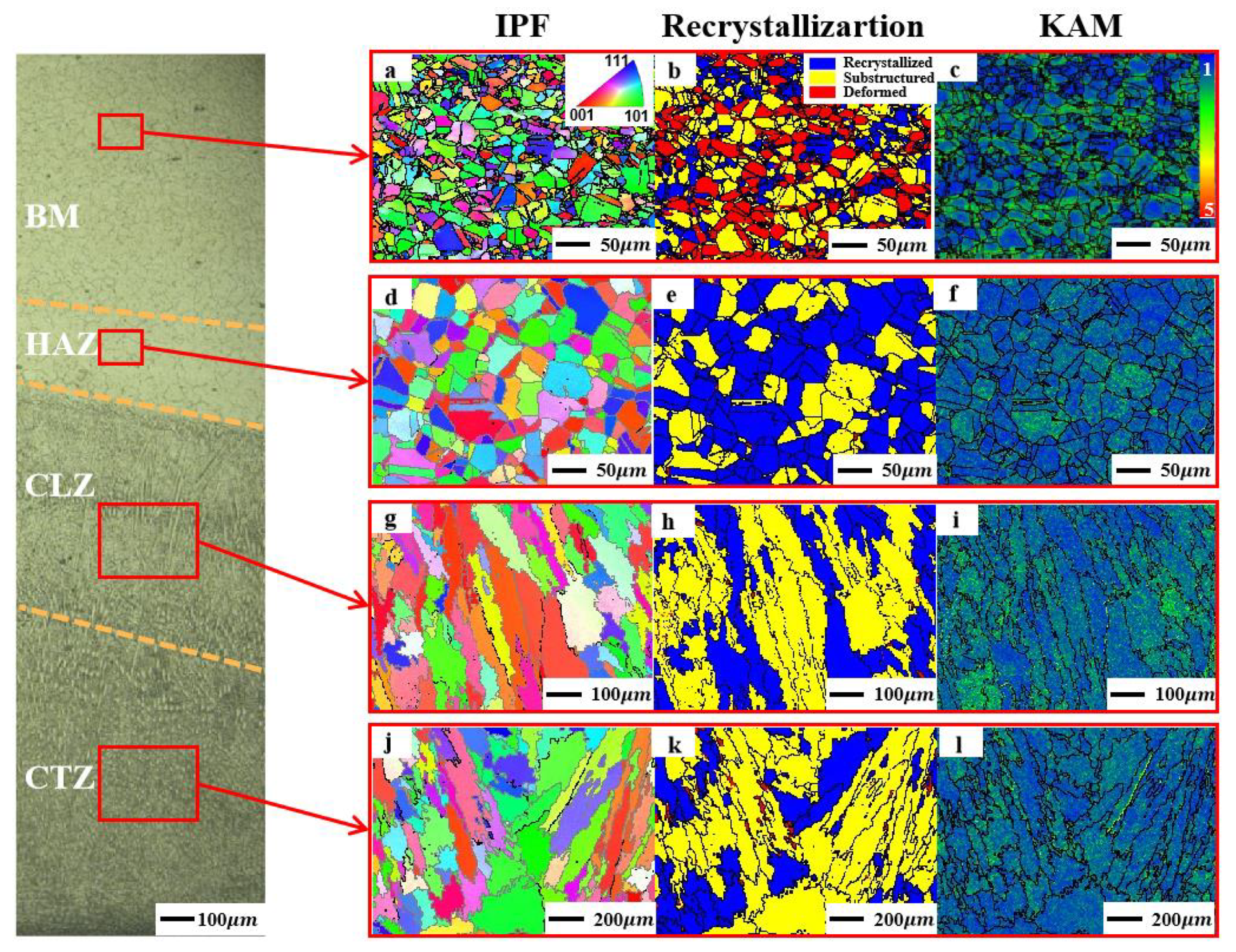
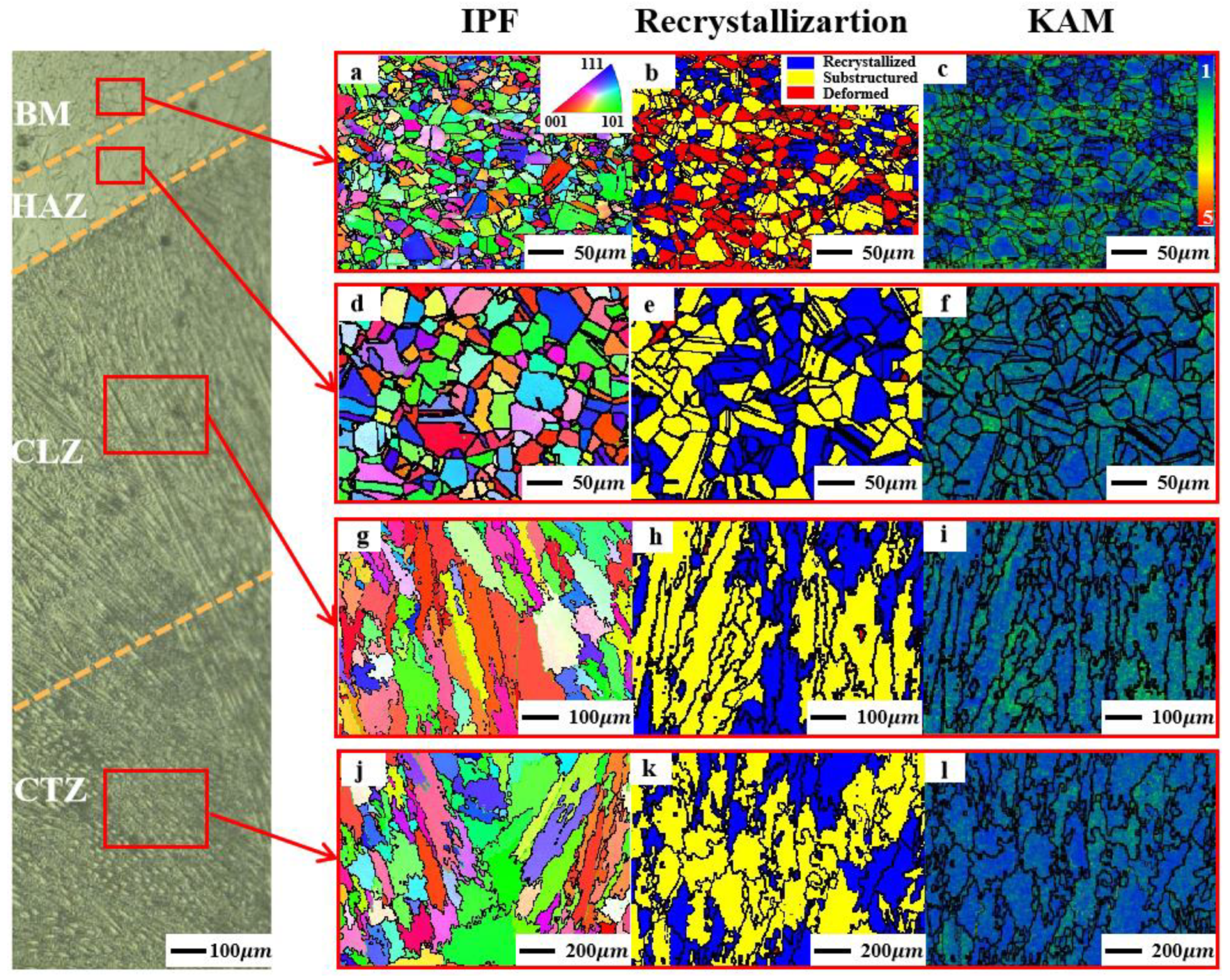
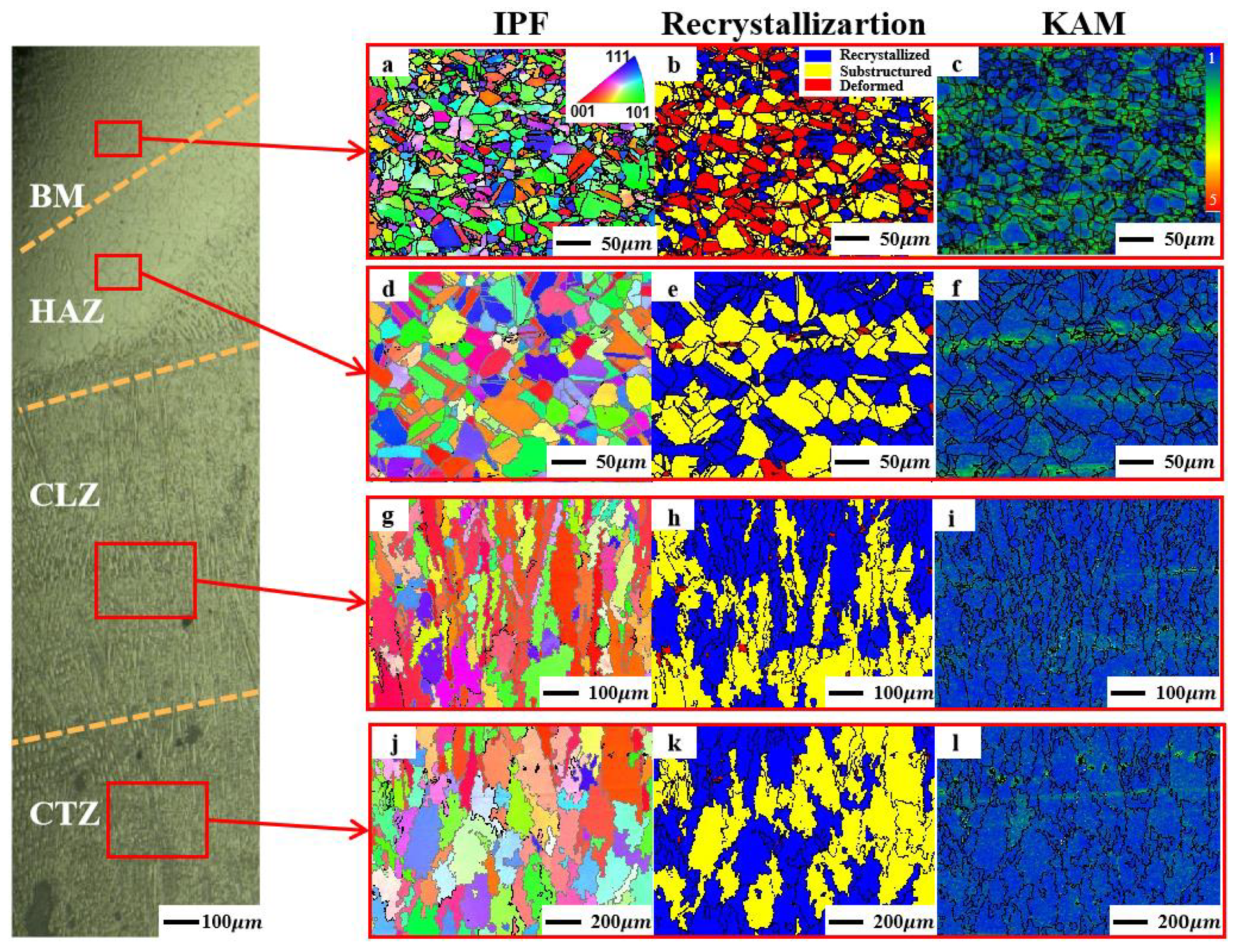
Figure 3, Figure 4, Figure 5 and Figure 6 show the IPF, recrystallization diagram, and kernel average misorientation (KAM) diagram of Inconel 625 nickel-base alloy samples in different areas under different focusing currents. Figure 3, Figure 4, Figure 5 and Figure 6a–l show the overall structural change of the austenite phase from BM to complete FZ. On the macroscale, the microstructure morphology of the Inconel 625 sample along the vertical direction is listed. Specifically, three subregions are selected, as shown on the left side of Figure 3, Figure 4, Figure 5 and Figure 6, including base metal (BM), heat affected zone (HAZ), and melting zone (FZ) [23]. In addition, considering the changes in growth and structural characteristics, the FZ is subdivided into the columnar zone (CLZ) and the central zone (CTZ) [23].
In Figure 3, Figure 4, Figure 5 and Figure 6, the horizontal direction is the same area, and different microstructure pictures, from left to right, are IPF pictures (a, d, g, j), Recrystallization diagram (b, e, h, k), and KAM diagram (e, f, i, l). In the vertical direction, from top to bottom, are the base metal area (BM) (a, b, c), the heat-affected zone (HAZ) (d, e, f), the melting columnar zone (CLZ) (g, h, i), and the melting center zone (CTZ) (g, h, i).
It can be seen from Figure 3, Figure 4, Figure 5 and Figure 6 that the austenite grains of Inconel 625 base metal (BM) are mainly equiaxed grains with an average grain size of 18 μ m and that there are a large number of twins. The grain orientation is mainly green {101} crystal plane and purple {111} crystal plane. Due to overheating of the high-energy electron beam molten pool, grain coarsening occurs in the melting zone (FZ) [24]. Partially melting characteristics are observed in the vicinity of FZ under the potential functions of the channeling effect and eutectic reaction [25]. CLZ presents strip grains, and CTZ presents island grains. In addition, the grain size of HAZ is obviously smaller than that of FZ, but the grains larger than those of the BM area are also equiaxed grains.
(b, e, h, k) in Figure 3, Figure 4, Figure 5 and Figure 6 are the recrystallization diagrams of microstructures in different regions. From the recrystallization diagram (b, e, h, k) in Figure 3, Figure 4, Figure 5 and Figure 6, it can be seen that there are a lot of red deformation areas in the original matrix structure and deformed grains. After electron beam surface modification, the heat-affected area and melting area become a yellow substructure area and a blue area, and the melting area has more yellow areas. When the focusing current is 700 mA~760 mA, there is little difference between the blue recrystallization area and the yellow substructure area in the melting column area (CLZ) and the melting center area (CTZ).
(c, f, i, l) in Figure 3, Figure 4, Figure 5 and Figure 6 shows the kernel average misorientation (KAM) diagram of microstructures in different regions. The KAM diagram is a qualitative representation of the degree of non-uniformity of material molding deformation and defect density distribution with the help of the Kernel Average Misorientation algorithm in EBSD. The recrystallization diagram (c, f, i, l) in Figure 3, Figure 4, Figure 5 and Figure 6 shows that after electron beam surface modification, the sample’s local orientation difference becomes relatively uniform, with only a few places showing high KAM values on the local grain boundary or in a small number of grains. From BM to CTZ, the KAM value of the microstructure of Inconel 625 nickel-base alloy tends to be more uniform. With the increase in electron beam focusing current (from 700 mA to 760 mA), the distribution of KAM values in the melting column region (CLZ) and the melting center region (CTZ) becomes more uniform. This may be because, with the increase of the focusing current, the melting area decreases and becomes relatively uniform.

3.3. Macroscopic Appearance of Wear Scar and Wear Volume

After the friction and wear test, a three-dimensional (3D) surface profiler based on white light interferometer scanning was used to measure the three-dimensional morphology of the worn surface of the sample. Figure 7 depicts the three-dimensional morphology and wear scar section curve of the Inconel 625 worn surface when subjected to the same load but using different focusing current scanning. It can be seen from Figure 7 that the substrate material is most severely worn, with the largest width and depth of wear marks, reaching 56 μm. After the electron beam strengthening treatment, the sample’s wear improved. According to the different wear macromorphologies, the process parameters have a greater impact on the wear scar. With the increase in electron beam focusing current, the maximum wear depth decreases first and then increases. The depth of the wear scar in a 720 mA sample is the minimum, and the depth of the wear scar is 43 μm. The depth of the wear scar in the 760 mA sample is the greatest, with a depth of 50 μm.
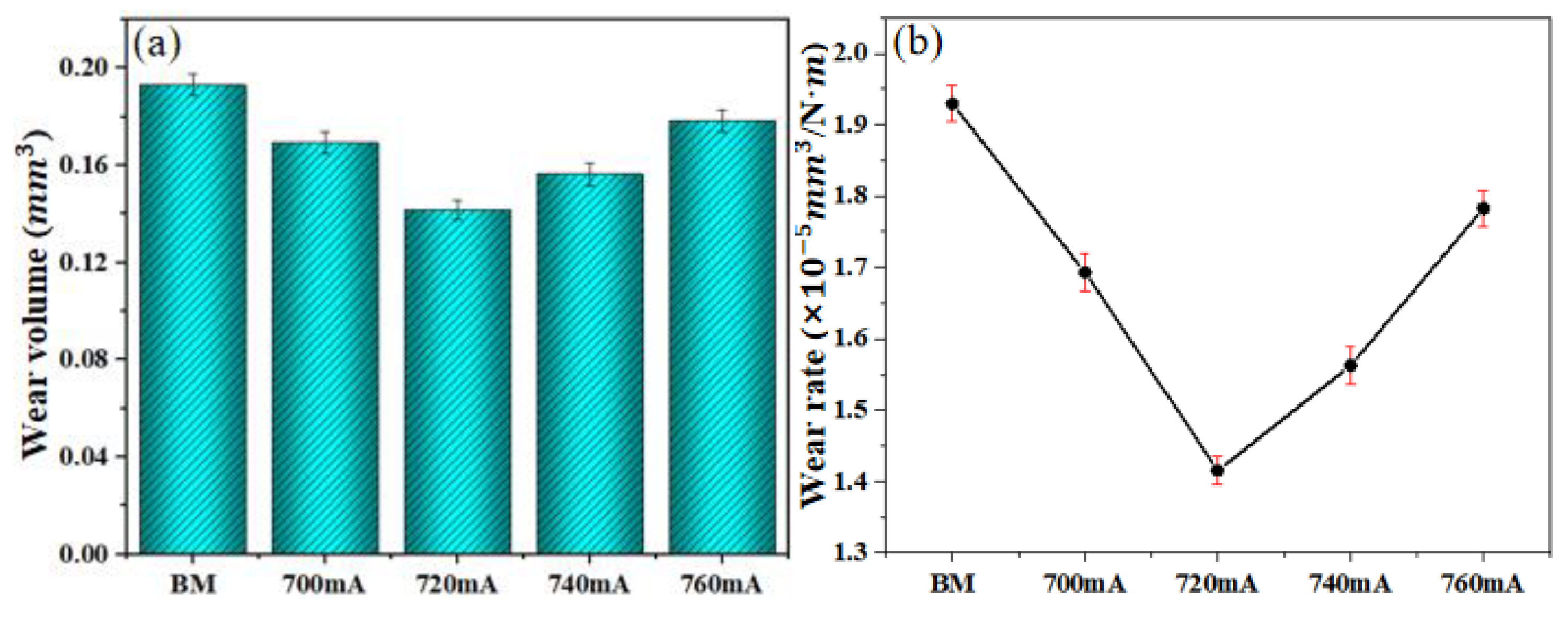
The wear volume was calculated by Gwyddion image analysis software. As shown in Figure 8, the minimum wear volume at 720 mA is 0.141525 mm 3 , and the maximum wear volume at the matrix is 0.192925 mm 3 . Compared with the Inconel 625 base metal, the 720 mA wear volume decreases by 26.64%. At 720 mA, the minimum wear rate is 1.41525 × 10 5   mm 3 / N · m , but the maximum wear rate of the Inconel 625 base metal is 1.92925 × 10 5   mm 3 / N · m . At 720 mA, compared with the Inconel 625 base metal, the wear rate decreased by 26.64%. Therefore, vacuum electron beam scanning treatment can improve the wear resistance of nickel-base alloys.

4. Discussion

4.1. Effect of Different Focusing Currents on Microstuction

Figure 9 shows the IPF, recrystallization, and KAM diagrams of the original Inconel 625. It can be seen from Figure 9 that the austenite grains of the original sample after thermal deformation mainly present equiaxed grains, with an average grain size of 18 μm, and there are a large number of twins. The grain orientation is mainly green {101} crystal plane and purple {111} crystal plane. This is because the {101} and {011} crystal planes of Inconel 625 have large energy storage during deformation and are easy to recrystallize and grow up during heating. This exactly corresponds to the recrystallization region and substructure region in Figure 9c.
According to Schwartz et al. [26], the kernel average misorientation (KAM) diagram can be used to determine the local strain level of grains. The blue trace of the KAM map represents the wrong supporting role of 0° (the lowest deformation degree), and the red map represents the wrong supporting role of 5 ° (the highest deformation degree). EBSD analysis can clearly identify the mechanism of microstructure change [27]. It can be seen from Figure 9d that after the original Inconel 625 sample is deformed, there is a large amount of dislocation defect density locally. There is a greater KAM color difference at the grain boundary. Compared with Figure 9c, it can be seen that the KAM value in the blue recrystallization area is smaller, and the KAM value in the red deformation area is larger. This is mainly because, for materials with low stacking fault energy, the dislocation density difference between grains is the driving force for recrystallization nucleation [28].
Figure 10 shows the IPF, recrystallization, and KAM diagrams of the thermal melting area of Inconel 625 under different focusing current scans. Different colors are used to indicate the grain orientation in the IPF diagram. It can be seen from Figure 10a,d,g,j that after electron beam scanning treatment of the original sample, the grains grow up, showing elongated grains and island grains. Under 720 mA to 760 mA focusing current, the melting zone presents an arc shape, while under 700 mA focusing current, the melting zone presents an inverted convex shape. This may be caused by the excessive electron beam energy breakdown of the substrate due to the small focusing current. It can be seen from the IPF diagram in Figure 10a,d,g,j that the austenite grain orientation in the melting area is mainly the red {001} crystal plane and the green {101} crystal plane.
Figure 10b,e,h,k shows the recrystallization diagram of the microstructure of the Inconel 625 hot melting area under different conditions. From Figure 10b,e,h,k, it can be seen that after electron beam scanning, the red deformation area of the matrix structure disappears, a large area of blue recrystallization area and yellow substructure area appear, and a local red deformation area exists. With the increase in focusing current, the blue recrystallization area decreases (700~740 mA). At 740 mA and 760 mA focusing current, the blue recrystallization region is stable. This is mainly due to the decrease of electron beam input energy with the increase of focusing current, which leads to a decrease in the driving force of grain boundary migration in the heat input process with the decrease of energy, thus slowing down the occurrence of recrystallization. Yaohui Song et al. [29] found similar findings in the influence of temperature on the thermal deformation and recrystallization behavior of nickel-base superalloys.
Figure 10c,f,i,l shows the KAM diagram of Inconel 625 microstructure under different conditions. The local orientation difference of the sample becomes relatively uniform after electron beam scanning, as shown in Figure 10a,c,f,i,l, with only a few exceptions, such as a small amount of high KAM values on the local grain boundary or in a small number of grains. With the decrease of the focusing current, the KAM value becomes more and more uniform.
The original Inconel 625 sample structure presents equiaxed austenite grains with an average grain size of about 18 μ m (Figure 9). It can be seen from Figure 10a,d,g,j that after electron beam scanning treatment of the original sample, the grains grow up, showing elongated grains and island grains. Under a 700 mA focused current, the melting zone presents an inverted convex shape, and the columnar grains in the melting zone are coarse, showing coarse columnar crystals. The maximum columnar crystal size is 400 μ m in long diameter and 150 μ m in short diameter. Under a 720 mA focused current, the columnar crystals in the melting zone become fine, showing slender columnar crystals. The average diameter of columnar crystals is about 300 μ m long and 60   μ m short. Under a 740 mA–760 mA focusing current, the length of columnar crystal in the melting zone becomes shorter, and the average length diameter of columnar crystal is about 150 μ m , and the short diameter is about 60 μ m . The grain size decreases with the increase of electron beam focusing current, which is mainly due to the decrease in energy input due to the increase in focusing current.
After the electron beam strengthening treatment, the sample’s wear improved. This may be related to the columnar crystals produced in the melting area. In particular, the depth of wear scar in the 720 mA sample is the smallest, and the depth of wear scar is 43 μ m . The minimum wear volume at 720 mA is 0.141525 mm 3 , and the maximum wear volume at the base is 0.192925. Compared with the original sample, the wear volume at 720 mA decreases by 26.64%. This is a relatively fine columnar crystal in the melting zone when 720 mA of focusing current is applied.
In other papers, columnar crystals have a great influence on wear resistance. Helin studied the wear resistance of 28% Cr cast iron in different directions in the columnar grain zone using abrasives of different hardness [30]. When a medium-hard abrasive was used, the carbide fibers arranged perpendicular to the wear surface would reduce the wear resistance of cast iron. When a low-hardness abrasive was used, the carbide fibers arranged perpendicular to the wear surface significantly improved the wear resistance of cast iron. Jianxun Mu prepared biocompatible TiZrNb films on biomedical Ti6Al4V substrates by DC magnetron sputtering [31]. TiZrNb thin films were deposited from hexagonal-phase and cube-phase columnar crystals by optimizing the sputtering power, effectively improving their wear resistance and corrosion resistance. The films deposited at 120 W with the largest grain size had the lowest wear loss and wear rate, which were 1.2 mg and 7.5 × 10 4 mm 3 / Nm , respectively, compared with the uncoated substrate, and were effectively reduced by 65.7% and 34.2%, respectively.

4.2. Effects of Different Focusing Currents on Texture

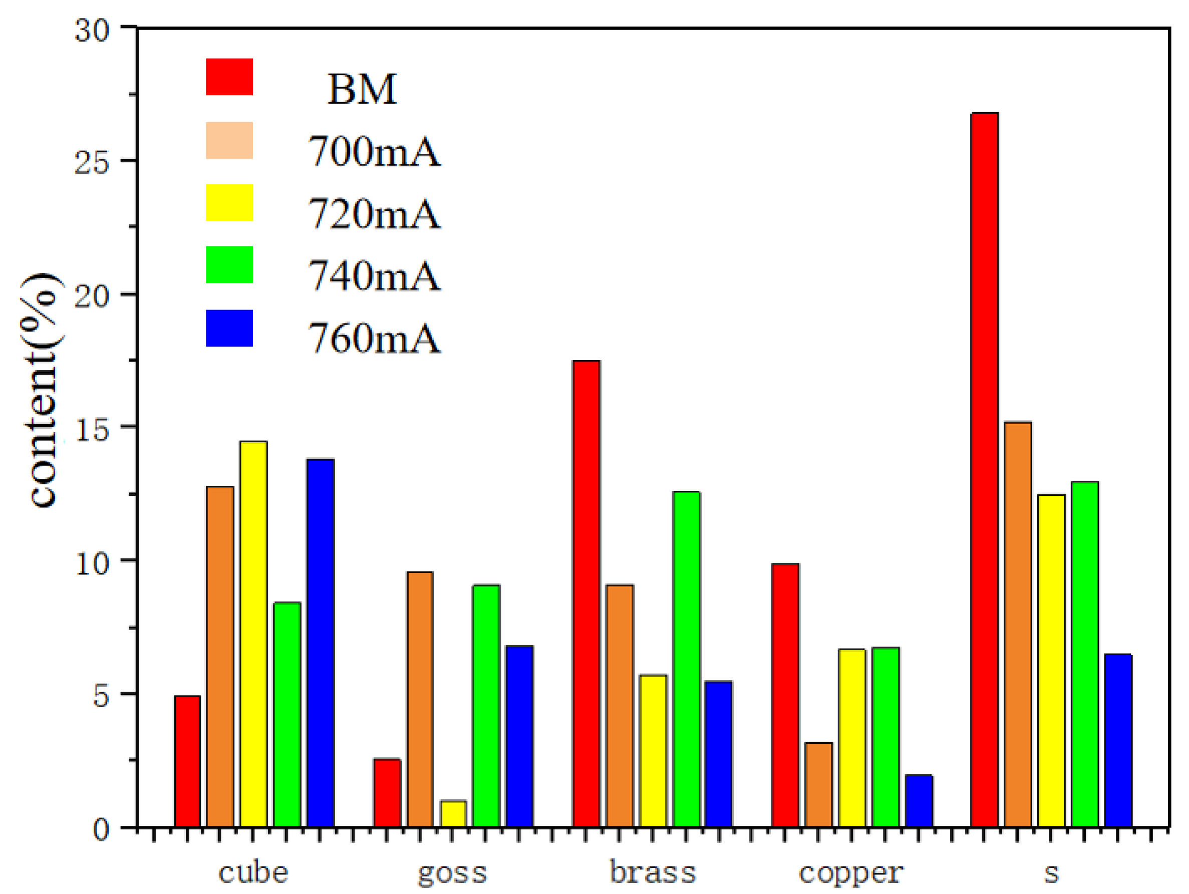
Figure 11 shows an ODF screenshot of the original Inconel 625 sample and the sample after the electron beam strengthening treatment ( φ 2 = 0°, 45°, 60°). The Euler angle is obtained from the ODF intercepted graph and then converted to the corresponding plate texture representation. It can be seen from Figure 11 that the austenite texture in its original state is concentrated in the Brass {110}<112> and S {123}<634>texture orientations. When the focusing current is 700 mA, the texture orientation becomes dispersed, and most grains are closer to <001> in the rolling direction, that is, closer to the Cube {001}<100> orientation. With the increase of the focusing current to 720 mA, the preferred orientation of grains is further enhanced, and the textures are concentrated in the Cube {001}<100>and S {123}<634> textures. When the focusing current is 740 mA, the Cube {001}<100> texture weakens, the Brass {110}<112> texture and the S {123}<634> texture increase, and there is some Goss {110}<001> texture and Copper {112}<111> texture. At 760 mA, the texture is concentrated in Cube {001}<100>, with minor amounts of Goss {110}<001>, Brass {110}<112>, and S {123}<634>. In general, electron beam scanning improves the Cube {001}<100> texture while weakening the Brass {110}<112> texture and the S {123}<634> texture. When the focusing current is 720 mA, the texture intensity of Cube {001}<100> reaches its highest value.
Figure 12 shows the content statistics of austenite texture of Inconel 625 original sample and sample in melting area after 700 mA to 760 mA electron beam scanning. The original samples are primarily S {123}<634> and Brass {110}<112>. S {123}<634> was the most common, accounting for 26.4% of them. The texture types of the melting zone in Inconel 625 changed to some extent under different focusing currents, but eventually, they all form a typical cubic texture; that is, the Cube {001}<100> texture and the S {123}<634> texture are the main textures (the content is about 10%), accompanied by a small amount of Brass {110}<112> and Copper {112}<111> textures. The content of the Cube {001}<100> texture in the melting area reaches 14.7% under 720 mA focusing. The <001> axis of the crystal usually grows along the direction of the maximum temperature gradient. The molten metal was prone to producing the Cube {001}<100> texture, and the S {123}<634> texture was a stable texture [32]. Therefore, after electron beam surface melting modification, the main textures are the Cube {001}<100> texture and S {123}<634> texture.
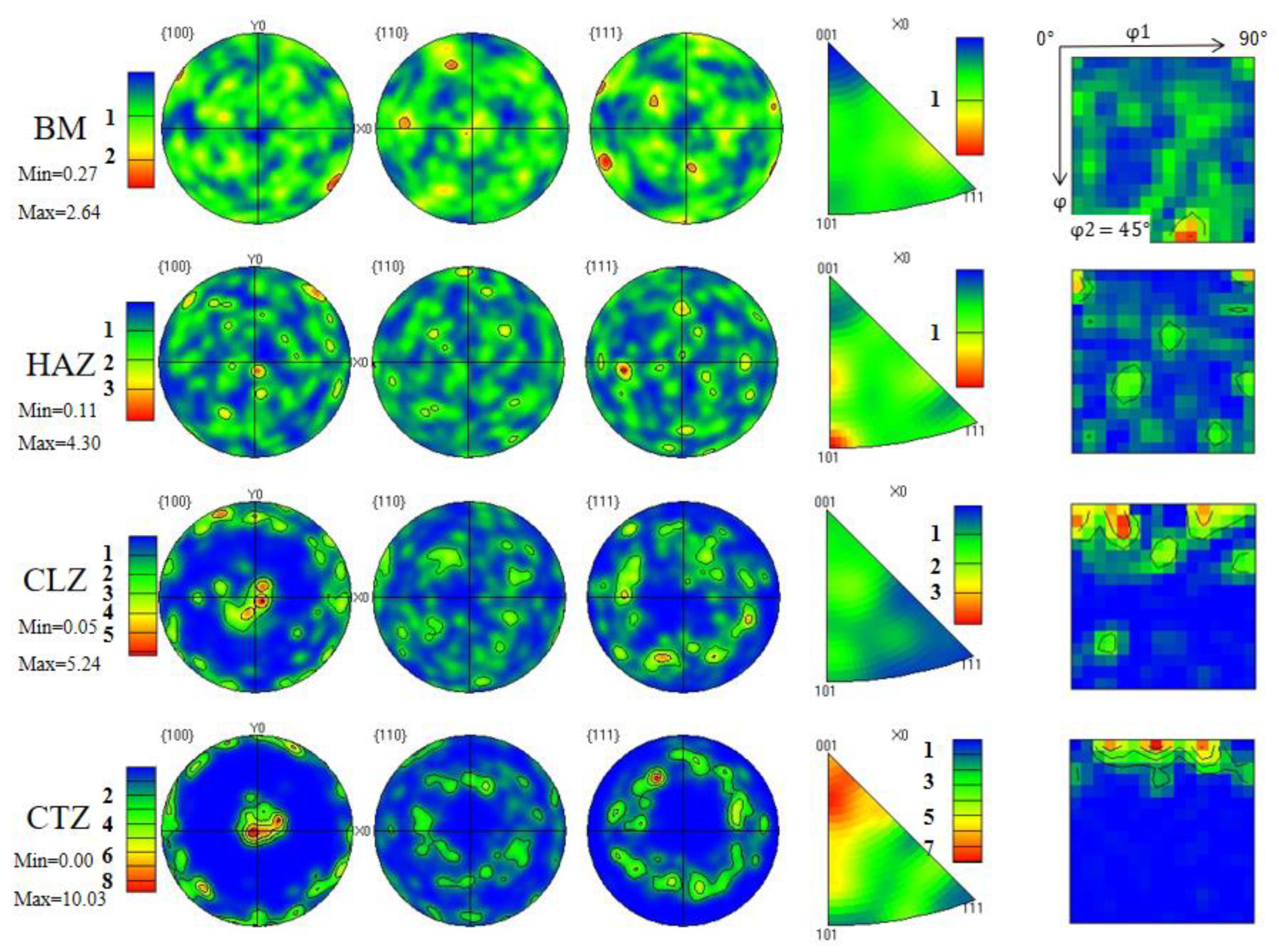
The orientation of different areas of the 720 mA sample was analyzed. The texture changes from the matrix to the melting zone were studied. Figure 13 depicts the corresponding pole diagram, reverse pole diagram, and ODF diagram for each area of the sample after scanning with a 720 mA electron beam ( φ 2 = 45°). It can be seen from the figure that FCC also has some textures in the BM part of Inconel 625, mainly Brass {110}<112>. In the HAZ region, the same texture is relatively dispersed. However, compared with BM, the FCC phase texture changes to {110} plane. In the CLZ region, a strong texture is formed in the austenite. The main components of these texture components are the Cube {001}<100> texture, and there is a trend of transformation to the rotted Cube {001}<110> texture. In the CTZ region, the texture of Cube {001}<100> is enhanced, which is the main texture.

4.3. Observation and Analysis of Wear Morphology

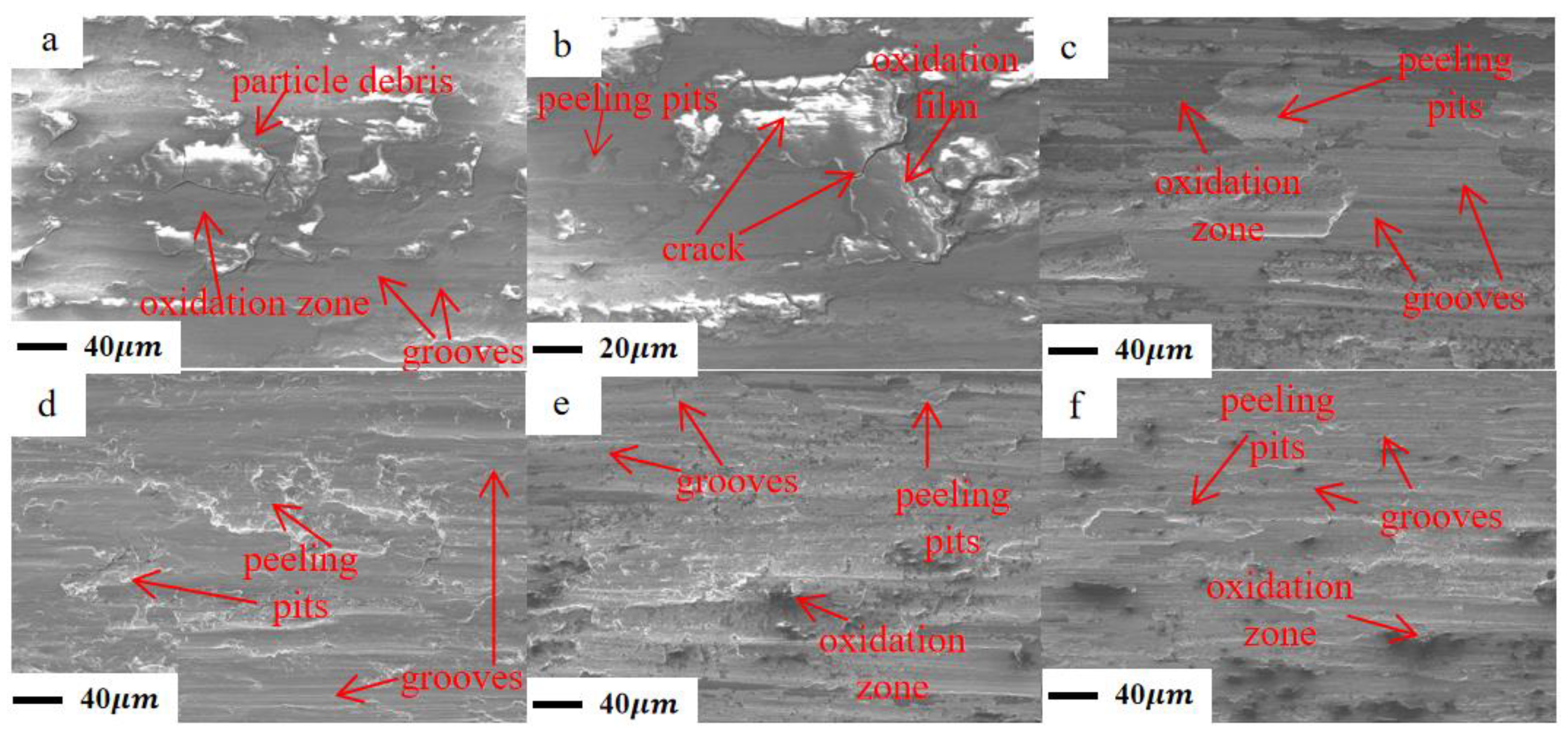
Figure 14 shows SEM images of worn surfaces under different specimens. It can be seen from Figure 14 that the wear surface of the sample is distributed with peeling pits of different depths and areas, reflecting the fatigue wear mechanism. The thin and shallow furrows parallel to the sliding direction indicate that there is weak abrasive wear. With the increase of friction time, the new surface produced by the peeling off of the wear oxidation area expands, the peeling pits and cracks on the surface increase, and the oxidation wear intensifies, resulting in the reduction of the distribution of oxygen elements in Figure 15.
The wear debris particles around the peeling pit increase, and the wear of the abrasive particles increases. Obvious cracks and peeling pits can be observed in Figure 14a,b, and the surface roughness increases. The wear surface in Figure 14a,b is covered with a layer of scale layer oxide film, which is formed by the rolling and fusion of flaky wear debris generated by intensified fatigue wear. Some flaky edges are raised under the action of alternating contact stress, and obvious cracks are generated. The wear debris particles scatter on the surface and participate in the three-body wear, making the furrow marks more obvious. The main wear mechanisms of nickel-base alloys under dry friction are adhesive wear, fatigue wear, and oxidation wear. However, in Figure 14c–f, the pear groove is more obvious, and no large-area oxidation area or crack are observed, indicating that the fatigue wear and oxidation wear of the material are reduced after electron beam scanning treatment.
Figure 15 shows the element distribution of the worn surface of the original material and the 720 mA surface-strengthened material under dry friction conditions. From Figure 15, it can be seen that the wear surface is covered with a large number of oxygen and silicon elements, indicating that the wear surface has oxidation behavior, which is consistent with the dark area in the electronic image. The surface oxygen element of the material treated by a 720 mA electron beam is slightly lower than that of the original Inconel 625 material, indicating that the surface oxidation wear is reduced after strengthening. The presence of silicon indicates that there is material migration between the nickel-base alloy and ceramic ball, which is a typical adhesive wear feature. Additionally, the surface silicon element after 720 mA electron beam scanning is obviously less than that of the original Inconel 625 material, indicating that the surface adhesion wear is reduced after strengthening. This is consistent with the findings in Figure 14.

5. Conclusions

The surface modification of Inconel 625 nickel-base alloy by vacuum electron beam scanning with different focusing currents was carried out, and the effect of focusing current on the microstructure and wear properties were studied. The results were as follows:
(1)
The austenite grains of the original sample after hot deformation mainly showed equiaxed grains with an average grain size of 18 μm, and there were a large number of twins. The grain orientation was mainly green {101} crystal plane and purple {111} crystal plane. After electron beam scanning, the grains of the original sample grew up, showing long strip grains and island grains. The melting zone was arc-shaped under a 720 mA to 760 mA focusing current. Under a 700 mA focused current, the melting zone presented an inverted convex shape. This was due to the small focusing current, which led to excessive electron beam energy breakdown of the substrate. The austenite grain orientation in the melting region was mainly red {001} crystal plane and green {101} crystal plane.
(2)
The wear volume of the original sample was the largest, 0.1929 mm 3 , and the wear rate was also the largest, 1.9292 × 10 5 mm 3 / N · m . After the electron beam strengthening treatment, the sample’s wear improved. With the increase in focusing current, the wear resistance decreased at first and then increased. At a 720 mA focusing current, the wear volume reached the minimum value of 0.1415 mm3, and the wear rate was also the minimum, which was 1.4153 × 10 5 mm 3 / N · m . Compared with the original sample, the 720 mA wear volume decreased by 26.64%. This may be related to the columnar crystals produced in the melting area. When a 720 mA focusing current was applied, relatively fine columnar crystals were found in the melting zone. After the electron beam scanning treatment, the fatigue wear, adhesive wear, and oxidation wear of the samples were improved to varying degrees.
(3)
The original Inconel 625 samples were mostly S {123}<634> and Brass {110}<112>. S {123}<634> was the most common, accounting for 26.4% of them. The texture types of the melting zone in Inconel 625 had changed to some extent under different focusing currents. However, they eventually all formed a typical cubic texture, the Cube {001}<100> texture and the S {123}<634> texture (the content was about 10%), accompanied by a small amount of Brass {110}<112> and Copper {112}<111> textures. The melting area contained 14.7% Cube {001}<100> texture under a 720 mA focusing current.

Author Contributions

J.L. (Juan Li): Conceptualization, Validation, Investigation, Writing—review and editing, Visualization, Supervision. J.Y.: Conceptualization, Methodology, Investigation, Writing—original draft. G.Z.: Investigation, Writing—review and editing, Supervision. H.L.: Conceptualization, Writing—review and editing, Visualization. Y.L.: Investigation, Writing—original draft, Formal analysis. J.L. (Jie Liu): Investigation. All authors have read and agreed to the published version of the manuscript.

Funding

The project was supported by the Fundamental Research Program of Shanxi Province (20210302123207 and 20210302124009), Scientific and Technological Innovation Programs of Higher Education Institutions in Shanxi (2021L292), Taiyuan University of Science and Technology Scientific Research Initial Funding (20212026), Taiyuan University of Science and Technology Graduate Innovation Project (BY2022004 and SY2022088) and the Coordinative Innovation Center of Taiyuan Heavy Machinery Equipment.

Institutional Review Board Statement

Not applicable.

Informed Consent Statement

Not applicable.

Data Availability Statement

All the data corresponding to the research are presented in the articles in Tabular or in graphical form.

Acknowledgments

All authors have read and agreed to the published version of the manuscript.

Conflicts of Interest

The authors declare no conflict of interest.

References

  1. Paul, C.P.; Ganesh, P.; Mishra, S.K.; Bhargava, P.; Negi, J.; Nath, A.K. Investigating laser rapid manufacturing for Inconel-625 components. Opt. Laser Technol. 2007, 39, 800–805. [Google Scholar] [CrossRef]
  2. Zhang, Y.; Jiang, Y.; Hu, X. Microstructure and high temperature creep properties of laser welded joints of Inconel 625 alloy formed by selective laser melting. J. Weld. 2020, 41, 78-84, 101–102. [Google Scholar]
  3. Kulka, M.; Makuch, N.; Dziarski, P. A study of nanoindentation for mechanical characterization of chromium and nickel borides’ mixtures formed by laser boriding. Ceram. Int. 2014, 40, 6083–6094. [Google Scholar] [CrossRef]
  4. Ueda, N.; Mizukoshi, T.; Demizu, K.; Sone, T.; Ikenaga, A.; Kawamoto, M. Boriding of nickel by the powder-pack method. Surf. Coat. Technol. 2000, 126, 25–30. [Google Scholar] [CrossRef]
  5. Deng, T.; Zheng, Z.; Li, J.; Xiong, Y.; Li, J. Surface polishing of AISI 304 stainless steel with micro plasma beam irradiation. Appl. Surf. Sci. 2019, 476, 796–805. [Google Scholar] [CrossRef]
  6. Qu, W.; Yang, B.; Liu, Y.; Yuan, K.; Kong, H.; Song, Y. Development and status quo of laser surface processing technology. Hot Work. Proc. 2017, 46, 38–41. [Google Scholar]
  7. Wang, J. Microstructure and Properties of 304 Austenitic Stainless Steel Modified by Electron Beam; Chongqing University of Technology: Chongqing, China, 2019; p. 8. [Google Scholar]
  8. Won, S.J.; Kim, H.S. Effects of laser parameters on morphological change and surface properties of aluminum alloy in masked laser surface texturing. J. Manuf. Proc. 2019, 48, 260–269. [Google Scholar] [CrossRef]
  9. Sharma, S.K.; Biswas, K.; Majumdar, J.D. Wear behaviour of Electron beam surface melted Inconel 718. Procedia Manuf. 2019, 35, 866–873. [Google Scholar] [CrossRef]
  10. Yang, S.; Wang, Y.; Shen, D.; Dong, W.; Wang, F. Research status onelectron beam of non-ferrous alloy. Mater. Rep. 2014, 28, 60–63. [Google Scholar]
  11. Liu, J.; Zou, Z.; Su, B. Reject High-Energy Beam Heat Treatment, 1st ed; China Machine Press: Beijing, China, 1997. [Google Scholar]
  12. Cai, J.; Lv, P.; Zhang, C.L.; Wu, J.; Li, C.; Guan, Q.F. Microstructure and properties of low carbon steel after surface alloying induced by high current pulsed electron beam. Nucl. Instrum. Methods Phys. Res. Sect. B Beam Interact. Mater. At. 2017, 410, 47–52. [Google Scholar] [CrossRef]
  13. Yang, S.; Guo, Z.; Zhao, L.; Guan, Q.; Zhao, L.; Liu, Y. Microstructures and corrosion resistance of Zircaloy-4 after surface alloying with copper by high-current pulsed electron beam. Appl. Surf. Sci. 2020, 501, 144222. [Google Scholar] [CrossRef]
  14. Vivek, P.; Akash, S.; James, H.; Mike, C.; David, H.; Wayne, H. Electron beam welding of In-conel 718. Procedia Manuf. 2020, 48, 428–435. [Google Scholar]
  15. Zhang, J.; Guan, Z. Electron beam welding process of Incoloy 825 nickel base superalloy and analysis of joint microstructure and mechanical properties. J. Weld. 2020, 41, 32–37. [Google Scholar]
  16. Ivanov, Y.F.; Ozur, G.E. Pulsed electron-beam treatment of WC–Ti C–Co hard-alloy cutting tools: Wear resistance and microstructural evolution. Surf. Coat. Technol. 2000, 125, 251–256. [Google Scholar] [CrossRef]
  17. Shu, D.; Cui, X.; Li, Z.; Sun, J.; Wang, G.; Si, W.; Dai, S.; Chen, X. Microstructure and friction and wear properties of nano-WC reinforced Ni-based coating. Adv. Laser Optoelectron. Progress. 2020, 57, 1–16. [Google Scholar]
  18. Kim, J.; Kim, J.; Kang, E.; Park, H.W. Surface modification of the metal plates using continuous electron beam process (CEBP). Appl. Surf. Sci. 2014, 311, 201–207. [Google Scholar] [CrossRef]
  19. Fu, Y.; Hu, J.; Shen, X.; Wang, Y.; Zhao, W. Surface hardening of 30CrMnSiA steel using continuous electron beam. Nucl. Instrum. Methods Phys. Res. Sect. B Beam Interact. Mater. At. 2017, 410, 207–214. [Google Scholar] [CrossRef]
  20. Wang, S.; Li, H.; Xu, H.B.; Chen, Y. Research progress on surface alloying based on high energy beams. South. Met. 2013, 5, 1–4+9. [Google Scholar]
  21. Zhang, F.; Wang, F.; Hao, J.; Ma, Y.; Ma, A. Three-beam surface modification technology application and development trends. Hebei Agric. Univ. J. 2003, 26, 260–263,266. [Google Scholar]
  22. Nippes, E.F. The weld heat-affected zone. Weld. J. 1959, 38, 15–185. [Google Scholar]
  23. Savage, W.; Nippes, E.; Szekeres, E. Study of weld interface phenomena in a low alloy steel. Weld. J. 1976, 55, 260. [Google Scholar]
  24. St Węglowski, M.; Błacha, S.; Phillips, A. Electron beam welding—Techniques and trends—Review. Vacuum 2016, 130, 72–92. [Google Scholar] [CrossRef]
  25. Zhu, Z.; Ma, X.; Mi, G.; Wang, C. Electron microscopy study of laser welded GH909 superalloy joint—ScienceDirect. J. Mater. Res. Technol. 2020, 9, 15525–15536. [Google Scholar] [CrossRef]
  26. Schwartz, A.J.; Kumar, M.; Adams, B.L.; Field, D.P. Electron Backscatter Diffraction in Materials Science; Springer: New York, NY, USA, 2009. [Google Scholar] [CrossRef]
  27. Babaniaris, S.; Ramajayam, M.; Jiang, L.; Varma, R.; Langan, T.; Dorin, T. Effect of Al3(Sc,Zr) dispersoids on the hot deformation behaviour of 6 xxx-series alloys: A physically based constitutive model. Mater. Sci. Eng. A 2020, 793, 139873. [Google Scholar] [CrossRef]
  28. Gavard, L.; Montheillet, F.; Coze, J.L. The effect of purity on dynamic recrystallization in austenitic stainless steels. Mater. Trans. JIM 2007, 41, 113–115. [Google Scholar] [CrossRef] [Green Version]
  29. Song, Y.; Li, Y. Hot deformation and recrystallization behavior of a new nickel-base superalloy for ultra-supercritical applications8. J. Mater. Res. Technol. 2022, 19, 4308–4324. [Google Scholar] [CrossRef]
  30. He, L.; Zhang, C. Study on wear resistance of as cast high chromium cast iron in columnar grain zone. Mech. Eng. Mater. 1998, 22, 4. [Google Scholar]
  31. Mu, J.; Wang, H.; Qin, B.; Zhang, Y.; Chen, L.; Zeng, C. Improved wear and corrosion resistance of biological compatible TiZrNb films on biomedical Ti6Al4V substrates by optimizing sputtering power. Surf. Coat. Technol. 2021, 428, 127866. [Google Scholar] [CrossRef]
  32. Zhao, G.; Sun, M.; Li, J.; Li, H.; Ma, L.; Li, Y. Study on quasi-in-situ tensile microstructure evolution law of 5052-O aluminum alloy based on EBSD. Mater. Today Commun. 2022, 33, 104572. [Google Scholar] [CrossRef]
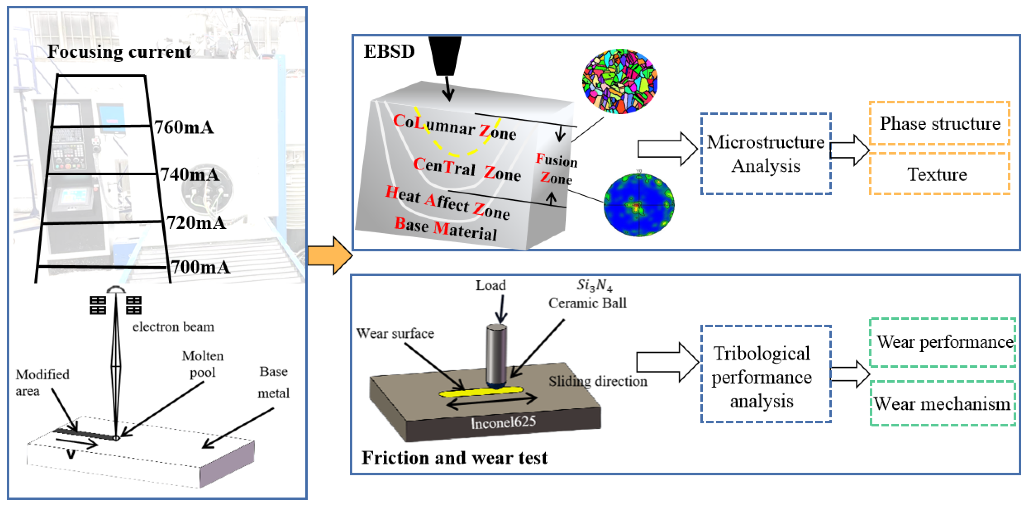
Figure 1. Experimental Flow Chart.
Crystals 13 00325 g001
Figure 2. Surface morphology of Inconel 625 nickel-base alloy after electron beam surface strengthening with different process parameters: (a) 700 mA, (b) 720 mA, (c) 740 mA, (d) 760 mA.
Crystals 13 00325 g002
Figure 3. The IPF, recrystallization diagram, and kernel average misorientation (KAM) diagram of different areas of the sample after 700 mA electron beam scanning: (ac) BM, (df) HAZ, (gi) CLZ, (jl) CTZ.
Crystals 13 00325 g003
Figure 4. The IPF, recrystallization diagram, and kernel average misorientation (KAM) diagram of different areas of the sample after 720 mA electron beam scanning: (ac) BM, (df) HAZ, (gi) CLZ, (jl) CTZ.
Crystals 13 00325 g004
Figure 5. The IPF, recrystallization diagram, and kernel average misorientation (KAM) diagram of different areas of the sample after 740 mA electron beam scanning: (ac) BM, (df) HAZ, (gi) CLZ, (jl) CTZ.
Crystals 13 00325 g005
Figure 6. The IPF, recrystallization diagram, and kernel average misorientation (KAM) diagram of different areas of the sample after 760 mA electron beam scanning: (ac) BM, (df) HAZ, (gi) CLZ, (jl) CTZ.
Crystals 13 00325 g006
Figure 7. Three-dimensional morphology and cross-section curve of the wear surface under different conditions: (a) Base metal, (b) 700 mA, (c) 720 mA, (d) 740 mA, and (e) 760 mA.
Crystals 13 00325 g007
Figure 8. Nickel-base alloy wear results from differently focused current electron beam scanning: (a) Wear Volume, (b) Wear Rate.
Crystals 13 00325 g008
Figure 9. IPF, recrystallization, and KAM diagrams of the original Inconel 625 base metal: (a) BM, (b) IPF, (c) Recrystallizartion, (d) KAM.
Crystals 13 00325 g009
Figure 10. Inconel 625 IPF, recrystallization, and KAM diagrams under different focusing current scanning conditions: (ac) 700 mA; (df) 720 mA; (gi) 740 mA; (jl) 760 mA.
Crystals 13 00325 g010
Figure 11. Distribution of austenite texture of Inconel 625 base material and specimens after 700 mA to 760 mA electron beam scanning.
Crystals 13 00325 g011
Figure 12. Austenite Texture Content of Inconel 625 Original Sample and Sample after Electron Beam Scanning at 700 mA to 760 mA.
Crystals 13 00325 g012
Figure 13. Corresponding pole diagram, reverse pole diagram, and ODF diagram of each area of the sample after 720 mA electron beam scanning ( φ 2 = 45°).
Crystals 13 00325 g013
Figure 14. SEM Image of Wear Surface under Different Specimens: (a) and (b) base metal, (c) 700 mA, (d) 720 mA, (e) 740 mA, (f) 760 mA.
Crystals 13 00325 g014
Figure 15. Dry Friction Surface Scanning Distribution of O and Si Elements on Inconel 625 Wear Surface (ac) base material; (df) 720 mA.
Crystals 13 00325 g015
Table 1. Inconel 625 chemical composition (mass fraction,%).
NiCrMoNbFeCNTiAl
61.922.88.43.42.20.90.10.10.1
Table 2. Electron beam scanning process parameters.
Beam CurrentFocusing CurrentAccelerating VoltageScanning Speed
10 mA700 mA60 KV240 mm/min
10 mA720 mA60 KV240 mm/min
10 mA740 mA60 KV240 mm/min
10 mA760 mA60 KV240 mm/min
Disclaimer/Publisher’s Note: The statements, opinions and data contained in all publications are solely those of the individual author(s) and contributor(s) and not of MDPI and/or the editor(s). MDPI and/or the editor(s) disclaim responsibility for any injury to people or property resulting from any ideas, methods, instructions or products referred to in the content.