Article

Trapped Carrier Recombination in Sb2Se3 Polycrystalline Film

1
College of Physics Science and Technology, Hebei University, Baoding 071002, China
2
Hebei Key Laboratory of Optic-Electronic Information Materials, Baoding 071002, China
3
Hebei Provincial Center for Optical Sensing Innovations, Baoding 071002, China
*
Authors to whom correspondence should be addressed.
Crystals 2023, 13(3), 406; https://doi.org/10.3390/cryst13030406
Submission received: 14 February 2023 / Revised: 22 February 2023 / Accepted: 24 February 2023 / Published: 27 February 2023
(This article belongs to the Topic Optoelectronic Materials)

Abstract

:
Sb2Se3 has recently emerged as a promising material for optic-electronic applications. In this work, trapped carrier recombination in Sb2Se3 was investigated by joint use of time-resolved microwave conductivity (TRMC) and photoluminescence (PL) spectroscopy. trapped carrier thermal excitation into the continuous band was observed in TRMC kinetics. Based on the exponential band tail model, the depth of the trap state, where trapped carriers are released into a continuous band, was estimated to range from 33.0 meV to 110.0 meV at room temperature. Temperature-varying TRMC and PL were further employed to study the influence of temperature on the trapped carrier recombination. Negative thermal quenchings of PL intensity and quantity of thermal emission carriers were observed and can be well explained by the thermal excitation of deep trapped carriers into shallow trap states and the continuous band. Two thermal activation energies of 12.5 meV and 304.0 meV were also revealed. This work is helpful for understanding the trapped carrier recombination process in polycrystalline Sb2Se3 film.

1. Introduction

Sb2Se3 has emerged as an excellent material for applications such as photovoltaic cells, photo detectors, photo-electrochemical water splitting, and phase-change materials [1,2,3,4,5]. The attractive properties of Sb2Se3 for the above applications include a suitable band gap (1.0–1.2 eV) [6], a high absorption coefficient and decent carrier mobility [7,8]. The carrier recombination kinetics in Sb2Se3 intrinsically determine its performance in those applications. It is very important to explore the characteristics of photo-generated carrier recombination in Sb2Se3.The free-carrier lifetime in Sb2Se3 has been reported to be on the order of tens of picoseconds by use of transient absorption spectroscopy, time-resolved terahertz spectroscopy and time- and angle-resolved two-photon photoemission [9,10,11]. Carrier trapping has been viewed as the main mechanism for shortening free-carrier lifetime in Sb2Se3. Recently, self-trapping originating from electron–phonon coupling in Sb2Se3 has also been reported as the explanation of short free-carrier lifetime [12,13]. Though it is a binary semiconductor, Sb2Se3 shows complicated defect chemistry due to its low-symmetry crystal structure [14,15]. Following the free carrier recombination at a time scale of tens of picoseconds, trapped carrier recombination persists on a time scale from nanoseconds to microseconds. Exploring trapped carrier recombination is also important for fully understanding photophysical properties of Sb2Se3. However, the research work focusing trapped carrier recombination is still rare [11,16,17].
In this work, trapped carrier recombination in polycrystalline Sb2Se3 film was studied by use of time-resolved microwave conductivity (TRMC) and photoluminescence (PL). The slow-decay TRMC kinetics at nanosecond to microsecond time scale was attributed to a trapped carrier recombination process with thermal emission into the continuous band mechanism. The depth of the trap state where the trapped carrier was released into the continuous band was estimated through fitting the TRMC kinetics with the exponential band tail model. By use of temperature-varying TRMC and PL spectroscopy, the influence of temperature on trapped carrier recombination was also investigated.

2. Materials and Methods

2.1. Film Preparation

The polycrystalline Sb2Se3 studied in this work was prepared by use of injection vapor deposition (IVD) [18]. Because of the low transmission attenuation of microwaves through fused silica, the fused silica of 0.7 mm thickness was chosen as the substrate. The temperature of fused silica was set at 480 °C. The high-purity Sb2Se3 (99.999%) was kept in a rotating roller of 390 °C. Sb2Se3 vapor was carried to the heated substrate by the injection of argon gas and deposited on the substrate.

2.2. Steady-State Photoluminescence Measurement

In temperature-varying photoluminescence (PL) measurement, Sb2Se3 film was mounted in a closed-cycle cryostat (Janis, CCS-150, USA) with temperature variable from 10 to 300 K. A CW 532 nm laser diode was used to excite Sb2Se3 film, and the emission was detected by a liquid-nitrogen-cooled CCD detector array (Princeton Instrument, PyLoN:1024-1.7, USA) attached to an spectrometer (Acton SP2500, USA).

2.3. Time-Resolved Microwave Conductivity Measurement

The photoconductance kinetics of Sb2Se3 film were measured in the open-cell model. The detailed information on TRMC setup can be found in Ref. [19]. An ITO glass was used as a microwave reflector, which led microwaves to pass the Sb2Se3 film twice. The distance between ITO film and Sb2Se3 film was carefully adjusted to ensure Sb2Se3 film was at the antinode of microwave. The output of Ti: Sapphire laser (800 nm, 100 fs, New Port, Spfire ACE-100F, Spectra Physics, USA) was frequency-doubled to excite free carriers in Sb2Se3 film. For temperature-varying TRMC measurement, Sb2Se3 film was mounted in liquid nitrogen cryostat (Oxford Instrument, UK).

2.4. Femtosecond Time-Resolved Reflectivity Measurement

The surface transient reflectivity of polycrystalline Sb2Se3 film was measured by using a transient absorption setup (Light conversion, Harpia, Lithuania) in the reflectivity mode. The fundamental output of Ti: Sapphire laser (800 nm, 100 fs) was delivered into an optical parameter amplification system (TOPAS Prime-F) to generate 650 nm pump pulse for Sb2Se3 film.

2.5. Structure and Morphology Measurement

The thickness of Sb2Se3 film was measured to be about 600 nm by use of Surface Profiler (Bruker, Dektak XT, USA). The ultraviolet–visible (UV–vis) absorption spectra were recorded by U4100 (Hitachi, U4100, Japan). The morphology of the films was observed by high-resolution field-emission scanning electron microscopy (SEM)(FEI, Nova NanoSEM 450, Czech). The X-ray diffraction (XRD) patterns were measured by a D/max 2400 X-ray diffractometer (Bruker, D8 ADVANCE, Germany) with Cu Kα radiation (λ = 1.54050 Å).

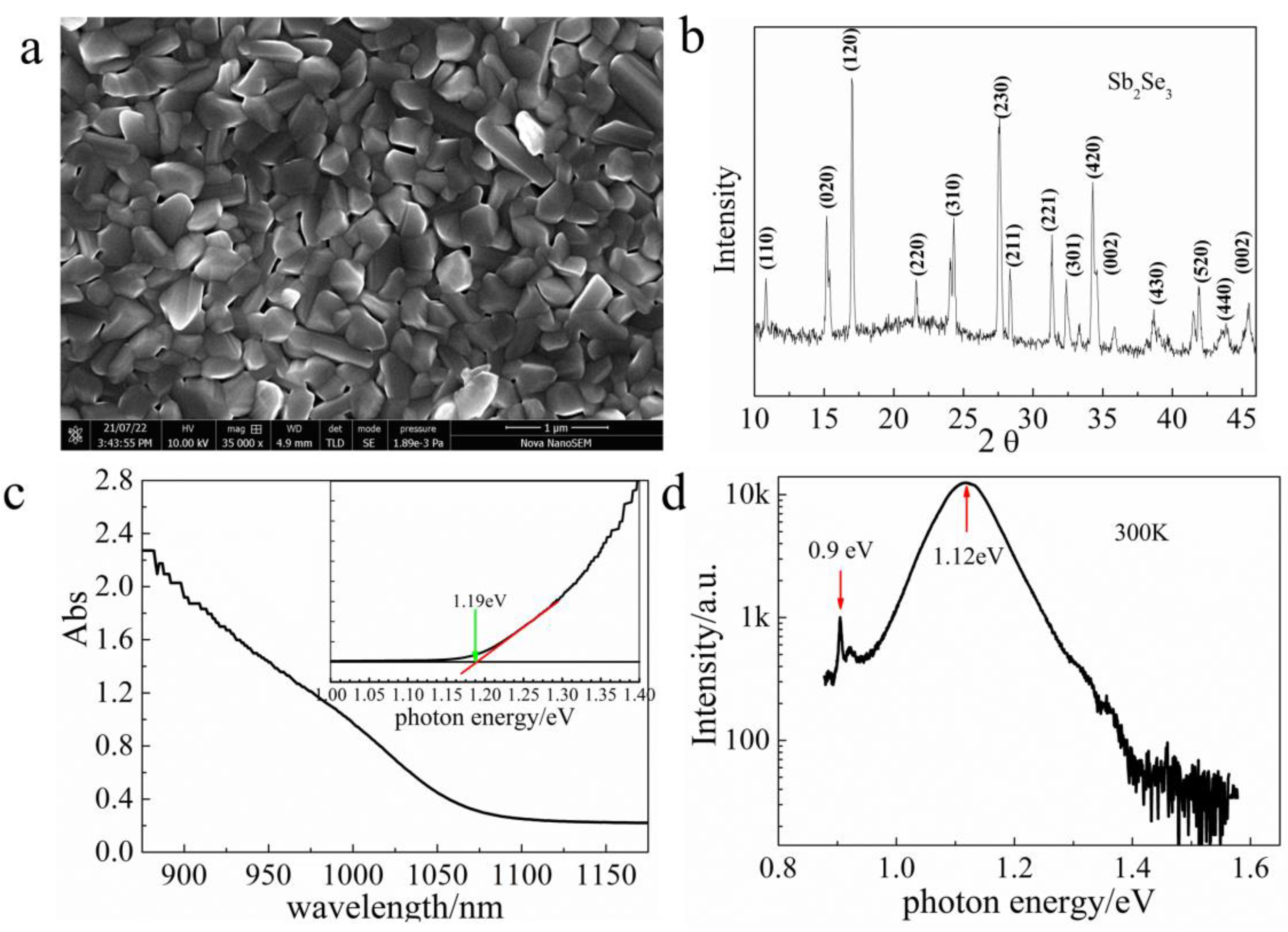
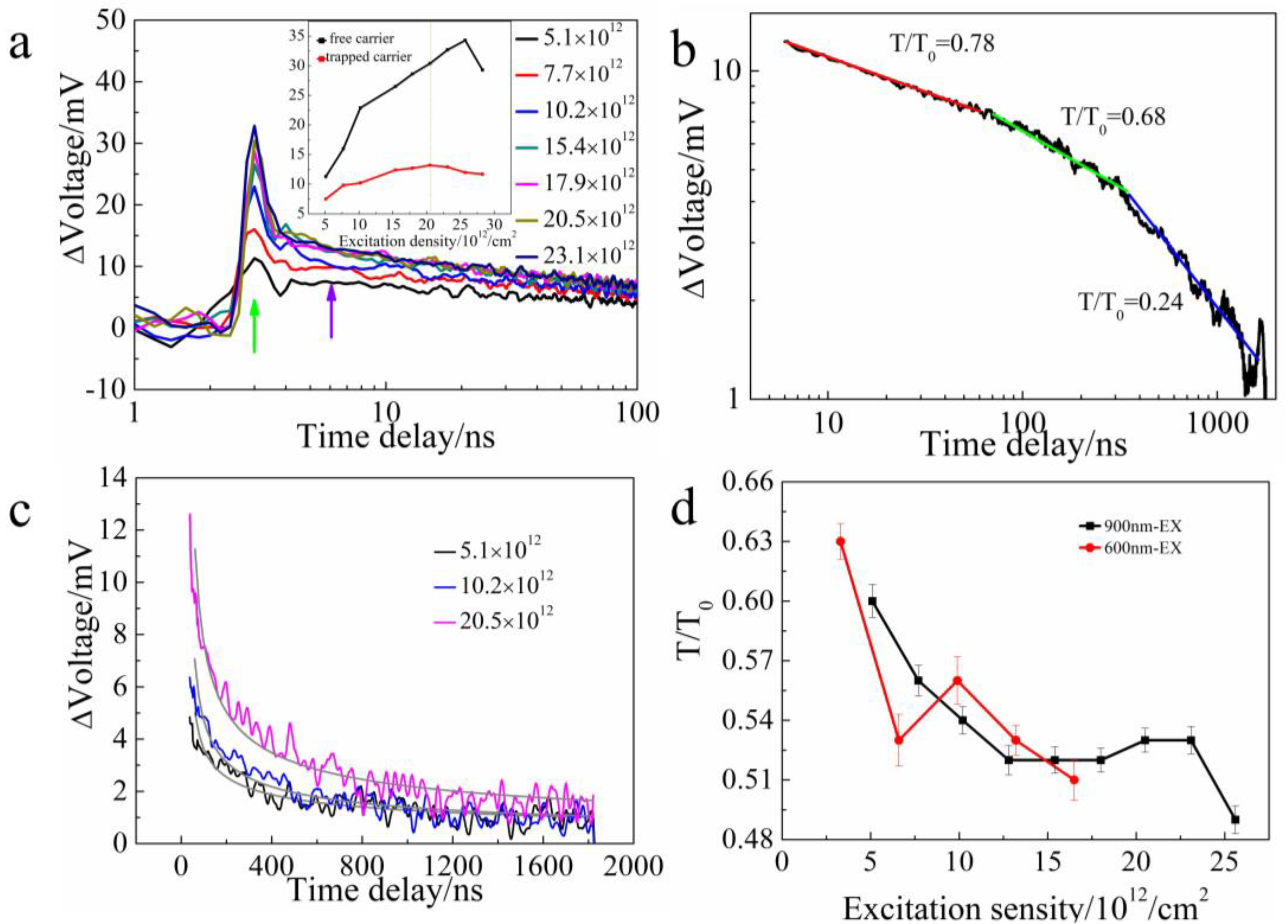
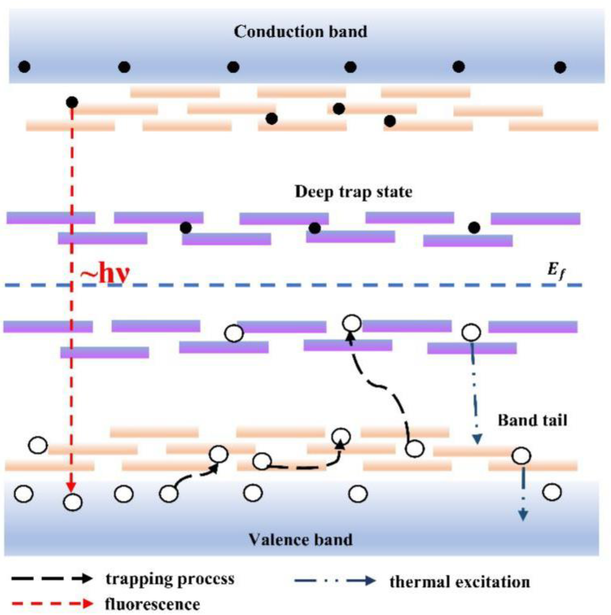
3. Results and Discussions

Top-view SEM (Figure 1a) and cross-section-view SEM (Figure S1 see Supplementary Materials) confirm the polycrystalline characteristic of Sb2Se3 film. Sb4Se6 ribbons randomly align, and the average diameter of ribbon was estimated to be about 100 ~ 200 nm. Figure 1b shows the XRD pattern of Sb2Se3 film. All the diffraction peaks’ positions agree well with the standard diffraction pattern of orthorhombic phase c-Sb2Se3 (JCPDS No: 015-0861). Diffraction peaks (120), (230) and (240) are the strongest among all diffraction peaks, meaning the orientation of quasi-one-dimensional [Sb4Se6]n is preferred to be parallel to the fused silica substrate. The absorbance of Sb2Se3 film is presented in Figure 1c. According to Tauc’s method, the band gap Eg of Sb2Se3 film was calculated to be 1.19 eV, which is close to the reported band gap of Sb2Se3 [6]. The PL spectrum of polycrystalline Sb2Se3 (Figure 1d) shows a main peak at about 1.12 eV and a weaker peak at 0.9 eV. Because of the red shift of the main peak with band-gap decrease (see temperature-varying PL experiment), we attribute the main peak to a free-to-shallow-bound-state recombination or shallow donor and acceptor pair recombination. Meanwhile, the position of the weak peak does not change as the band gap changes, so it possibly originates from a deep trap state. Recently, Zhu et al. attributed this weak peak to carrier self-trapping due to electron and phonon coupling [13].
We investigate the charge recombination kinetics of polycrystalline Sb2Se3 by TRMC technique. In TRMC measurement, free charge carriers are generated in a semiconductor by a short laser pulse, giving rise to a light-induced change in the conductance in the sample. The change in conductance in the sample over time is traced with the power of the reflected microwave and is displayed by the oscillograph. Assuming that the carrier mobility does not change during the time window of our measurement, the decrease in the photoconductance with time is purely due to concentration reduction in mobile carriers in the conduction and valance band.
The TRMC kinetic curves of Sb2Se3 show two parts, i.e., a fast-decay part and a slow-decay part (Figure 2a and Figure S2). This indicates that charge recombination occurs in Sb2Se3 via two different mechanisms. The fast decay meets the instrument response of our TRMC setup. Assuming the instrument response of the TRMC setup is a Gaussian function, the time resolution is characterized as the Full-Width Half-Magnitude (FWHM), which is about 0.3 ns. The reported free carrier lifetime of Sb2Se3 is shorter than the time resolution of the TRMC setup, so the measured kinetics of free carrier recombination are very similar to the instrument response [11,20]. Following the free carrier recombination, a slower recombination process appears with about a 2.0 ns time delay after the carrier generation (marked by green arrow in Figure 2a). The slower recombination process occurs on a nanosecond to microsecond time scale. Considering the very short free carrier lifetime in Sb2Se3, it is reasonable to attribute this slower carrier recombination to the trapped carrier recombination process. Under thermal activation, trapped carriers are released into the conduction band and valance band, inducing a photoconductance response. The TRMC signal amplitude of the slowing decay part is proportional to the thermal emission carrier quantity and also proportional to the trapped carrier quantity. We extracted the free-carrier-related TRMC signal (marked by green arrow) and trapped-carrier-related TRMC signal (marked by purple arrow) from TRMC kinetics curves. The inset of Figure 2a displays their amplitudes at different excitation densities. As excitation density increases, the TRMC signal of thermal emission trapped carriers firstly saturates, confirming the limiting trap state density where trapped carriers thermally release.
The evolution of thermal emission carrier quantity from trap states is determined by the trap state distribution in the forbidden band. According to small stokes shifts of main PL with respect to the band gap Eg of Sb2Se3, the band tail should be present near the conduction band and valance band. The trapped carrier in the band tail should be responsible for slower recombination process revealed by TRMC. To estimate the distribution of trap states where trapped carriers thermally release, we employ an exponential distribution band tail model, where trap state density reduces exponentially with the gap between the trap state and continuous band (Equation (1)) [21].
g ( E ) e x p [ ( E 0 E k B T 0 ) ]
where k B is the Boltzmann constant, T is thermodynamic temperature, E is the energy of the trap state, E 0 is the bottom energy of the conduction band (take electron trap state, for example), and k B T 0 is the scale energy of exponential distribution of the band tail. In the case of exponential band tail distribution of the trap state, the evolution of thermal emission carrier quantity n ( t ) with time can be described by Equation (2) [21]:
n ( t ) t ( 1 T T 0 )
Figure 2b presents a TRMC kinetic curve related with a trapped carrier thermal emission process in log–log coordinates, and the slope of the curve would equal ( 1 T T 0 ) if the TRMC kinetic can be well described by Equation (2). However, we found the extracted T T 0 value changes at different time scale, i.e., T T 0 is 0.78 in the range of 2–60 ns time delay, 0.68 in the range of 60–330 ns time delay and 0.24 in the range of 330–1800 ns time delay. With T equal to 300 K, the scale energy of the band tail state k B T 0 was calculated to range from 33.0 meV to about 110.0 meV. Experimental results show that a thermal emission carrier is not released from a sole exponential band tail. Multiple kinds of trap states are involved in the trapped carrier thermal emission process. Here, we use the calculated scale energy k B T 0 to estimate trap state depth. The thermal emission trapped carrier mainly originates from trap states, with depth ranging from 33.0 meV to 110.0 meV.
We further examined the influence of excitation density on the trapped carrier thermal emission process. An averaged T T 0 was used to fit the TRMC kinetic curves with excitation wavelengths 900 nm (Figure 2c) and 600 nm (Figure S3), respectively. The extracted average T T 0 values (Figure 2d) reduce with excitation density increase in both excitation cases. The calculated trap depth extends from 40.0 meV to 51.6 meV as excitation density increases. It indicates that the trapped carrier occupies deeper trap states in a high-excitation-density condition.
To understand the trapped carrier recombination process in further detail, temperature-dependent TRMC kinetic curves of Sb2Se3 were measured. The sensitivity factor of the TRMC setup changes with temperature due to the variations of Sb2Se3 dielectric constant ε . Therefore, both carrier concentration and the sensitivity factor of the setup influence the amplitude of the TRMC signal at different temperatures. To compare the quantity of remaining trapped carriers in the Sb2Se3 film, we normalized the TRMC kinetic curves at different temperatures, and we show them from a 2 ns time delay after excitation in Figure 3a. After normalization, the amplitude of TRMC kinetic curves was proportional to the quantity of remaining trapped carriers or free carriers released from trap states. As shown in Figure 3a, the quantity of thermal emission carriers at 2 ns time delay after excitation obviously changes with temperature, and the minimum appears at about 150 K (inset of Figure 3a).
The quantity of thermal emission carriers is proportional to the product of N ( t ) ν ( T ) , where N ( t ) is trapped carrier concentration and ν ( T ) is the thermal emission probability. The thermal emission probability ν ( T ) is determined by both temperature T and trap depth E T , as shown in Equation (3) [21].
ν ( T ) = ν 0 exp ( E T k B T )
where ν 0 is the crystal lattice vibration frequency, E T is the energy depth of the trap state, and k B is the Boltzmann constant. According to Equation (3), a trapped carrier has a higher probability of being released as temperature increased. In the temperature range from 80 K to 150 K, the reduction in thermal emission carrier quantity should result from the decrease in trapped carrier concentration N ( t ) with temperature. This confirms that temperature increase accelerates the recombination of trapped carriers in the first 2 ns time delay after excitation. As temperature increases further from 150 K to 200 K, the quantity of thermal emission carriers shows a recovery. Despite the increase in thermal emission probability ν ( T ) , trapped carrier concentration N ( t ) is also likely to increase in this temperature range due to the population of trapped carriers from deeper trap states. As temperature exceeds 200 k, trapped carrier concentration N(t) decreases, which counteracts the effect of thermal emission probability ν ( T ) , so the quantity of thermal emission carriers does not show obvious change on the whole.
The effect of temperature on the evolution of the quantity of thermal emission carriers was also investigated. Two TRMC kinetics at 80 K and 120 K are compared in Figure 4. Obviously, the quantity of thermal emission carriers at 120 K decays more slowly with time. We suppose that deep trapped carrier thermal emission into a shallow trap state leads to the slower decay of thermal emission carrier quantity at high temperature. Average scale energy k B T 0 was also extracted by fitting the TRMC kinetics at different temperatures with Equation (2) (black line in Figure 3b). The scale energy k B T 0 can also be used to characterize the depth of the trap state, which involves a trapped carrier thermal emission process. The depth of these trap states is about 10.0 meV at 10 K. As temperature exceeds 250 K, the estimated trap depth shows obvious fluctuations due to a low signal–noise ratio of TRMC kinetics. At 300 K, the estimated depth of the trap state is about 60.0 meV. In a phonon-assisted carrier de-trap model, trapped carriers are released into the conduction band or valance band after receiving energy from thermal lattice vibrations [22,23,24]. The average phonon occupation number increases continuously with temperature, which favors the de-trap process of trapped carriers at deep trap states.
Temperature-dependent steady PL of Sb2Se3 was also measured for comparison with temperature-varying TRMC measurement. With temperature increases, the main peak (1.20 eV at 20 K) red-shifts (inset of Figure 3c), which consists in a change in band gap E g with temperature [25], while the position of the minor peak (0.9 eV at 20 K) does not change with temperature. In addition, the main peak is close to the band gap E g , i.e., 0.07 eV discrepancy at 300 K. Thus, the main peak possibly originates from band–shallow trapped carrier recombination or shallow donor–shallow acceptor pair recombination. In these two radiation mechanisms, the peak of PL correlates with the band gap Eg and the binding energy of the shallow trap state. Thus, the main PL peak red-shifts as the band gap Eg decreases. According to the FWHM of the main PL peak, the extension of radiative trap states into the forbidden band was estimated to be about 130.0 meV at 300 K.
The dependence of main peak intensity on temperature is presented in Figure 3d. As temperature increases from 20 K to 40 K, the PL intensity increases. In the temperature range from 40 K to 140 K, the PL intensity reduces monotonously. While temperature exceeds 140 K, the PL intensity increases again until about 220 K, at which point the PL intensity start to reduce again. The negative thermal quenching of PL in Sb2Se3 (140–220 K) has also been reported in other semiconductors, such as ZnO and FASnI3 [26,27]. In Sb2Se3 film, thermal excitation of a trapped carrier into a continuous band and a shallow trap state is the main mechanism of negative thermal quenching of PL [28]. In polycrystalline Sb2Se3, the negative thermal quenching of PL and TRMC coincides in the same temperature range.
Obviously, the thermal emission trapped carriers contribute to both the PL intensity and photoconductance. This further confirms our attribution of slow-decay TRMC kinetics to trapped carrier release into the conduction (valance) band. The recombination of these thermal emission carriers emits fluorescence photons at around the main PL peak. In further, by use of Arrhenius’ Equation (4), we estimated the thermal activation energy of non-radiative recombination with the main PL peak [28].
I ( T ) = I 0 1 + A e x p ( E T k B T )
where A is the process rate constant, and E T is the thermal activation energy of the non-radiative process. In the temperature ranges from 40 K to 140 K and from 220 K to 300 K, the two thermal activation energies E T are 12.5 meV and 304.0 meV (Figure 3d), respectively. Using temperature-varying femtosecond time-resolved reflectivity spectroscopy, we found the free-carrier recombination rate is independent of temperature (Figure S4). Ghosh also report that changing temperature nearly does not affect free-carrier recombination [29]. It is reasonable to deduce that thermal quenching of the PL peak in Sb2Se3 results from trapped carrier recombination. However, we cannot correlate the two thermal activation energies with trapped electrons or trapped holes directly at present.
PL of Sb2Se3 confirms the band tail near the continuous band. This band tail extends into the forbidden band by about 130.0 meV. The TRMC kinetic curve analysis reveals the trap energy depth ranging from 33.0 meV to 110.0 meV at room temperature. We suppose that TRMC and PL probe the same trapped carrier in this work. The band tail in polycrystalline Sb2Se3 film contains not only disorder-induced potential energy fluctuation but also some point defects. Theoretical calculation shows that SeSb antisites induce shallow acceptor energy [15,30,31], and its trap depth was measured to be 95 ~ 120 meV [7,32], even 53 meV in nanocrystalline-selenium-poor Sb2Se3 film [33]. Se vacancy Vse forms an electron trap state, which is reported to be located 0.4 eV below the conduction band [15,34]. The trap energy distribution revealed in this work is consistent with the reported results on the whole. Considering the complex defect chemistry, other electron defects and hole defects could also be present in polycrystalline Sb2Se3 film. In addition, we also checked the trap station distribution at film surface or bulk. We used the CdS to passivate the polycrystalline Sb2Se3 film. After passivation, the PL intensity increased by about 20 times, while the slower TRMC kinetics still persisted. This means that the trap state from which trapped carrier thermal emission also exists in the bulk of polycrystalline Sb2Se3 film.
We propose the scheme in Figure 4 to explain our experimental results. We take a hole as an example to illustrate carrier recombination. Similar recombination also occurs to electrons. All the photo-generated carriers in polycrystalline Sb2Se3 film would be captured by trap states or recombine radiatively in tens of picoseconds after excitation. The free-carrier recombination process induces the fast decay of our measured TRMC kinetic curves. The radiation recombination between free carriers and trapped carriers results in the main PL peak (1.12 eV at 300 K). A trapped hole can undergo uphill and downhill relaxation. The trapped hole recombination is thermally activated in temperature ranges of 40 K~140 K and 220 K~300 K. In the temperature range of about 140~220 K, the thermal excitation of trapped holes into the continuous band and shallow trapped states, leading to negative thermal quenching of PL and quantity of thermal emission carriers.

4. Conclusions

In this work, TRMC and PL were jointly used to study the trapped carrier recombination process in polycrystalline Sb2Se3 film. The same trap states in the forbidden band were probed by these two techniques. trapped carrier thermal excitation into a continuous band or more shallow trapped state is one important channel for trapped carrier recombination. Trapped carriers thermally excited into a continuous band lead to the slow decay of TRMC kinetics on a nanosecond to microsecond time scale. Based on the exponential band tail model, we estimated the depth of the trap state where trapped carriers are thermally excited into a continuous band. Our experimental results show that increasing the excitation density or increasing temperature enables more deep trapped carrier thermal emission into a continuous band. The trapped carrier thermal emission mechanism can also explain well the negative thermal quenching of PL intensity and quantity of thermal emission carriers in the temperature range from 140 K to 220 K. With temperature-varying PL measurement, we also observe two thermal activation energies of 12.5 meV and 304.0 meV for trapped carrier recombination. The free-carrier lifetime is short in Sb2Se3 film, and it is sensible to explore performance of trapped carriers in applications. Understanding trapped carrier recombination is vital to this aim. Our work provides insight into trapped carrier recombination in Sb2Se3 film.

Supplementary Materials

The following supporting information can be downloaded at: https://www.mdpi.com/article/10.3390/cryst13030406/s1, Figure S1: Cross section SEM of polycrystalline Sb2Se3 film; Figure S2: TRMC kinetic curves of Sb2Se3 under different excitation density (photons/cm2), excitation wavelength 600 nm; Figure S3: TRMC kinetic curves related with trapped carrier thermal emission process in microsecond timescale under different excitation density (photons/cm2) and their fittings (excitation wavelength 600 nm); Figure S4: Femtosecond surface transient reflectivity of polycrystalline Sb2Se3 film at some typical temperatures.

Author Contributions

Conceptualization, W.D. and Z.L.; methodology, W.D. and B.L.; software, W.D.; validation, W.D. and Y.G.; formal analysis, K.W. and X.Z.; investigation, T.T. and J.S.; resources, T.T. and J.S.; data curation, T.T. and J.S. and W.D.; writing—original draft preparation, W.D.; writing—review and editing, W.D. and Z.L.; visualization, J.S.; supervision, W.D. and Z.L.; project administration, W.D. and Z.L.; funding acquisition, Z.L. All authors have read and agreed to the published version of the manuscript.

Funding

This research was funded by Hebei Natural Science Foundation Project (F2017201136, F2020201051).

Conflicts of Interest

The authors declare no conflict of interest.

References

  1. Chen, C.; Li, K.; Tang, J. Ten years of Sb2Se3 thin film solar cells. Sol. RRL 2022, 6, 2200094. [Google Scholar] [CrossRef]
  2. Chen, S.; Liu, T.; Zheng, Z.; Ishaq, M.; Liang, G.; Fan, P.; Chen, T.; Tang, J. Recent progress and perspectives on Sb2Se3-based photocathodes for solar hydrogen production via photoelectrochemical water splitting. J. Energy Chem. 2022, 67, 508–523. [Google Scholar] [CrossRef]
  3. Müller, M.J.; Yadav, A.; Persch, C.; Wahl, S.; Hoff, F.; Wuttig, M. Tailoring crystallization kinetics of chalcogenides for photonic applications. Adv. Electron. Mater. 2022, 8, 2100974. [Google Scholar] [CrossRef]
  4. Singh, Y.; Kumar, M.; Yadav, R.; Kumar, A.; Rani, S.; Shashi; Singh, P.; Husale, S.; Singh; V. Enhanced photoconductivity performance of microrod-based Sb2Se3 device. Sol. Energy Mater. Sol. Cells 2022, 243, 111765. [Google Scholar] [CrossRef]
  5. Wan, P.; Jiang, M.; Su, L.; Xia, S.; Wei, Y.; Xu, T.; Liu, Y.; Shi, D.; Fang, X.; Kan, C. Perpendicularly Reversed Polarization Sensitivity of Double-faced Photodetection based on Sb2Se3 Microbelt. Adv. Funct. Mater. 2022, 32, 2207688. [Google Scholar] [CrossRef]
  6. Chen, C.; Li, W.; Zhou, Y.; Chen, C.; Luo, M.; Liu, X.; Zeng, K.; Yang, B.; Zhang, C.; Han, J.; et al. Optical properties of amorphous and polycrystalline Sb2Se3 thin films prepared by thermal evaporation. Appl. Phys. Lett. 2015, 107, 043905. [Google Scholar] [CrossRef]
  7. Chen, C.; Bobela, D.C.; Yang, Y.; Lu, S.; Zeng, K.; Ge, C.; Yang, B.; Gao, L.; Zhao, Y.; Beard, M.; et al. Characterization of basic physical properties of Sb2Se3 and its relevance for photovoltaics. Front. Optoelectron. 2017, 10, 18–30. [Google Scholar] [CrossRef]
  8. Hadke, S.; Huang, M.; Chen, C.; Tay, Y.F.; Chen, S.; Tang, J.; Wong, L. Emerging chalcogenide thin films for solar energy harvesting devices. Chem. Rev. 2021, 122, 10170–10265. [Google Scholar] [CrossRef]
  9. Chen, T.; Cao, R.; Cai, H.; Lian, W.; Tang, R.; Xiang, Y.; Wang, Y. Revealing the chemical structure-dependent carrier trapping in one-dimensional antimony selenide photovoltaic materials. J. Mater. Chem. A 2022, 10, 20482–20488. [Google Scholar] [CrossRef]
  10. Grad, L.; von Rohr, F.; Zhao, J.; Hengsberger, M.; Osterwalder, J. Photoexcited charge carrier dynamics in Sb 2 Se 3 (100). Phys. Rev. Mater. 2020, 4, 105404. [Google Scholar] [CrossRef]
  11. Wang, K.; Chen, C.; Liao, H.; Wang, S.; Tang, J.; Beard, M.C.; Yang, Y. Both free and trapped carriers contribute to photocurrent of Sb2Se3 solar cells. J. Phys. Chem. Lett. 2019, 10, 4881–4887. [Google Scholar] [CrossRef]
  12. Yang, Z.; Wang, X.; Chen, Y.; Zheng, Z.; Chen, Z.; Xu, W.; Liu, W.; Yang, Y.; Zhao, J.; Chen, T.; et al. Ultrafast self-trapping of photoexcited carriers sets the upper limit on antimony trisulfide photovoltaic devices. Nat. Commun. 2019, 10, 4540. [Google Scholar] [CrossRef] [PubMed] [Green Version]
  13. Tao, W.; Zhu, L.; Li, K.; Chen, C.; Chen, Y.; Li, Y.; Li, X.; Tang, J.; Shang, H.; Zhu, H. Coupled Electronic and Anharmonic Structural Dynamics for Carrier Self-Trapping in Photovoltaic Antimony Chalcogenides. Adv. Sci. 2022, 9, 2202154. [Google Scholar] [CrossRef]
  14. Lian, W.; Cao, R.; Li, G.; Cai, H.; Cai, Z.; Tang, R.; Zhu, C.; Yang, S.; Chen, T. Distinctive Deep-Level Defects in Non-Stoichiometric Sb2Se3 Photovoltaic Materials. Adv. Sci. 2022, 9, 2105268. [Google Scholar] [CrossRef] [PubMed]
  15. Huang, M.; Xu, P.; Han, D.; Tang, J.; Chen, S. Complicated and unconventional defect properties of the quasi-one-dimensional photovoltaic semiconductor Sb2Se3. ACS Appl. Mater. Interfaces 2019, 11, 15564–15572. [Google Scholar] [CrossRef] [PubMed]
  16. Prabhakar, R.R.; Moehl, T.; Friedrich, D.; Kunst, M.; Shukla, S.; Adeleye, D.; Damle, V.H.; Siol, S.; Cui, W.; Gouda, L.; et al. Sulfur treatment passivates bulk defects in Sb2Se3 photocathodes for water splitting. Adv. Funct. Mater. 2022, 32, 2112184. [Google Scholar] [CrossRef]
  17. Prabhakar, R.R.; Moehl, T.; Friedrich, D.; Kunst, M.; Shukla, S.; Adeleye, D.; Damle, V.H.; Siol, S.; Cui, W.; Gouda, L. Gouda, Unravelling Defect Passivation Mechanisms in Sulfur-Treated Sb2Se3; Cambridge University Press: Cambridge, UK, 2021. [Google Scholar] [CrossRef]
  18. Duan, Z.; Liang, X.; Feng, Y.; Ma, H.; Liang, B.; Wang, Y.; Luo, S.; Wang, S.; Schropp, R.E.I.; Mai, Y.; et al. Sb2Se3 Thin-Film Solar Cells Exceeding 10% Power Conversion Efficiency Enabled by Injection Vapor Deposition Technology. Adv. Mater. 2022, 34, 2202969. [Google Scholar] [CrossRef] [PubMed]
  19. Xiao, Z.; Tao, T.; Shu, J.; Dang, W.; Pan, S.; Zhang, W. Charge Carrier Recombination Dynamics in MAPb (Br1−yIy) 3 Single Crystals. Crystals 2022, 12, 1425. [Google Scholar] [CrossRef]
  20. Yang, W.; Lee, S.; Kwon, H.-C.; Tan, J.; Lee, H.; Park, J.; Oh, Y.; Choi, H.; Moon, J. Time-resolved observations of photo-generated charge-carrier dynamics in Sb2Se3 photocathodes for photoelectrochemical water splitting. ACS Nano 2018, 12, 11088–11097. [Google Scholar] [CrossRef]
  21. Orenstein, J.; Kastner, M. Thermalization and recombination in amorphous semiconductors. Solid State Commun. 1981, 40, 85–89. [Google Scholar] [CrossRef]
  22. Piana, G.M.; Bailey, C.G.; Lagoudakis, P.G. Phonon-Assisted Trapping and Re-excitation of Free Carriers and Excitons in Lead Halide Perovskites. J. Phys. Chem. C 2019, 123, 19429–19436. [Google Scholar] [CrossRef]
  23. Williams, C. Kinetics of trapping, detrapping, and trap generation. J. Electron. Mater. 1992, 21, 711–720. [Google Scholar] [CrossRef]
  24. Kagawa, T.; Matsumoto, N. Transient photocurrents in a-Si: H and weak electron-phonon coupling processes. Philos. Mag. B 1985, 51, 273–283. [Google Scholar] [CrossRef]
  25. Birkett, M.; Linhart, W.M.; Stoner, J.; Phillips, L.J.; Durose, K.; Alaria, J.; Major, J.D.; Kudrawiec, R.; Veal, T.D. Band gap temperature-dependence of close-space sublimation grown Sb2Se3 by photo-reflectance. Apl. Mater. 2018, 6, 084901. [Google Scholar] [CrossRef] [Green Version]
  26. Kahmann, S.; Nazarenko, O.; Shao, S.; Hordiichuk, O.; Kepenekian, M.; Even, J.; Kovalenko, M.V.; Blake, G.R.; Loi, M.A. Negative thermal quenching in FASnI3 perovskite single crystals and thin films. ACS Energy Lett. 2020, 5, 2512–2519. [Google Scholar] [CrossRef]
  27. Watanabe, M.; Sakai, M.; Shibata, H.; Satou, C.; Satou, S.; Shibayama, T.; Tampo, H.; Yamada, A.; Matsubara, K.; Sakurai, K.; et al. Negative thermal quenching of photoluminescence in ZnO. Phys. B Condens. Matter 2006, 376, 711–714. [Google Scholar] [CrossRef]
  28. Shibata, H. Negative thermal quenching curves in photoluminescence of solids. Jpn. J. Appl. Phys. 1998, 37, 550. [Google Scholar] [CrossRef]
  29. Singh, P.; Ghorai, N.; Thakur, A.; Ghosh, H.N. Temperature-dependent ultrafast charge carrier dynamics in amorphous and crystalline Sb2Se3 Thin Films. J. Phys. Chem. C 2021, 125, 5197−5206. [Google Scholar] [CrossRef]
  30. Savory, C.N.; Scanlon, D.O. The complex defect chemistry of antimony selenide. J. Mater. Chem. A 2019, 7, 10739–10744. [Google Scholar] [CrossRef] [Green Version]
  31. Liu, X.; Xiao, X.; Yang, Y.; Xue, D.-J.; Li, D.-B.; Chen, C.; Lu, S.; Gao, L.; He, Y.; Beard, M.C.; et al. Enhanced Sb2Se3 solar cell performance through theory-guided defect control. Prog. Photovolt. Res. Appl. 2017, 25, 861–870. [Google Scholar] [CrossRef]
  32. Cifuentes, N.; Ghosh, S.; Shongolova, A.; Correia, M.R.; Salomé, P.M.P.; Fernandes, P.A.; Ranjbar, S.; Garud, S.; Vermang, B.; Ribeiro, G.M.; et al. Electronic conduction mechanisms and defects in polycrystalline antimony selenide. J. Phys. Chem. C 2020, 124, 7677–7682. [Google Scholar] [CrossRef]
  33. González, J.C.; Limborço, H.; Ribeiro-Andrade, R.; Silva, B.C.; Krambrock, K. Deciphering the role of defects in the ambipolar electrical transport in nanocrystalline Sb2Se3 thin films. Adv. Electron. Mater. 2022, 8, 2100985. [Google Scholar] [CrossRef]
  34. Dong, S.; Sun, L.; Yue, F. Influence of selenium growth condition on the photovoltaic conversion efficiency of Sb2Se3 as the solar cell absorption layer. J. Mater. Sci. Mater. Electron. 2022, 33, 10335–10342. [Google Scholar] [CrossRef]
Figure 1. (a) Top-view SEM, (b) XRD, (c) optical absorbance and (d) photoluminescence of polycrystalline Sb2Se3 film. The inset of c is the direct band gap Tauc’s plot of Sb2Se3 film, and the red line is used for extrapolation.
Crystals 13 00406 g001
Figure 2. (a) TRMC kinetic curves of Sb2Se3 under different excitation densities (photons/cm2, excitation wavelength 900 nm); the inset of Figure 2a shows the dependence of TRMC signals amplitudes at photoexcitation (green arrow) and 3 ns time delay after excitation (purple arrow) on the excitation density. (b) TRMC kinetic curve related with the trapped carrier thermal emission recombination process (starting from 3 ns delay after excitation) and its fitting at different time scales, excitation density 15.4 × 10¹² photons/cm2. (c) TRMC kinetic curves related with trapped carrier thermal emission process at microsecond time scale under different excitation densities and their fittings (excitation wavelength 900 nm). (d) The dependence of T T 0 on the excitation density, 900 nm excitation–black square, 600 nm excitation–red circle.
Crystals 13 00406 g002
Figure 3. (a) Normalized TRMC kinetic curves of Sb2Se3 at different temperatures. Excitation wavelength 650 nm, excitation density 1.4 × 10 14 photons/cm2, time scale ranges from 2 ns after excitation to 180 ns. The inset of (a) shows the change in amplitude of normalized TRMC kinetic curves at 2 ns after excitation with temperature. (b) Normalized TRMC kinetic curves of Sb2Se3 at 80 K and 120 K and their fittings. The time scale ranges from 30 ns after excitation to 8000 ns after excitation; inset of (b) shows the dependence of scale energy k B T 0 on temperature. (c) Steady PL of Sb2Se3 at different temperatures (94.8W/cm2); the inset of (c) shows the main PL peak shifts with temperature. (d )shows the dependence of main PL integration area on temperature and its Arrhenius equation fitting.
Crystals 13 00406 g003
Figure 4. Schematic of carrier recombination dynamics in polycrystalline Sb2Se3 film. This schematic intentionally illustrates the hole recombination. Theoretically, a similar process also occurs to electrons.
Crystals 13 00406 g004
Disclaimer/Publisher’s Note: The statements, opinions and data contained in all publications are solely those of the individual author(s) and contributor(s) and not of MDPI and/or the editor(s). MDPI and/or the editor(s) disclaim responsibility for any injury to people or property resulting from any ideas, methods, instructions or products referred to in the content.

