Abstract
We report on the epitaxial lateral overgrowth (ELO) of high-quality AlN on stripe-patterned Si(111) substrates with various trench widths. By narrowing down the trench and ridge widths of patterned Si substrates, crack-free, 6-micrometer-thick, high-quality AlN films on Si substrates were produced. The full-width-at-half-maximum values of the X-ray-diffraction rocking curves for the AlN (0002) and (10) planes were as low as 260 and 374 arcsec, respectively, corresponding to a record low dislocation density of 1.3 × 109 cm−2. Through the combination of a micro-Raman study and the X-ray diffraction analysis, it was found that narrowing the stripe width from 5 μm to 3 μm can reduce the vertical growth thickness before coalescence, resulting in a large decrease in the internal tensile stress and tilt angle, and, therefore, better suppression in the cracks and dislocations of the ELO–AlN. This work paves the way for the fabrication of high-performance Al(Ga)N-based thin-film devices such as ultraviolet light-emitting diodes and AlN bulk acoustic resonators grown on Si.
1. Introduction
In recent years, AlN has attracted significant attention due to its excellent properties and potential applications, such as thin-film ultraviolet light-emitting diodes (UV LEDs) and thin-film bulk acoustic resonators [1,2,3,4]. Because of the limited size and extremely high cost of bulk AlN substrates, AlN crystals are always grown hetero-epitaxially on foreign substrates, such as sapphire and silicon (Si) [5,6,7,8]. The partial or full removal of the substrate is an essential step in the fabrication of bulk acoustic-wave devices, as well as thin-film flip-chip-structure UV LEDs, which have much higher light-extraction efficiency than typical UV LEDs [9,10,11]. However, the separation of sapphire substrates with AlN epilayers by the laser-lift-off process remains very challenging due to the laser-induced crystal damage [12,13]. In contrast, Si substrates can be easily removed by wet-chemical etching without damage. Moreover, Si substrates have advantages such as their low cost, large scale, high thermal conductivity, and potential for integration with electronics [14,15,16]. Therefore, the utilization of Si substrates to grow AlN has become one of the most promising approaches to the fabrication of AlN- and AlGaN-based thin-film devices.
However, the growth of high-quality AlN on Si substrates is highly challenging. Firstly, the large lattice mismatch (~19%) between AlN and Si(111) usually leads to a high threading-dislocation density (TDD, 1010~1011 cm−2) and initial tensile stress. Secondly, the huge thermal-expansion-coefficient mismatch (~43%) between AlN and Si results in appreciable tensile stress, which induces crack networks during cooling down to room temperature [17,18,19]. Therefore, the thickness of AlN films grown on Si was always limited to less than 1 μm to prevent cracks, which was insufficient to prevent dislocation and improve the AlN quality [20,21,22].
Epitaxial lateral overgrowth (ELO) has been demonstrated as an effective way to reduce cracks and TDD for AlN growth on Si [23,24,25]. Pioneering work by Zhang et al. demonstrated a 7-micrometer-thick, fully coalesced AlN layer on Si(111) by ELO, and, therefore, a thin-film flip-chip UV LED [26]. Moreover, Tran et al., from Riken, reported an 8-micrometer-thick ELO–AlN on a patterned Si substrate [27]. Nonetheless, the reported full width at half maxima (FWHM) of the X-ray diffraction (XRD) rocking curves for AlN (10) planes are as high as 800 arcsec, which is far from the demands of device-quality AlN on Si [28,29,30,31].
In this work, we carefully studied the ELO of AlN on stripe-period patterned Si(111) substrates with various trench widths. By narrowing down the period width of the patterned Si substrates, crack-free, 6-micrometer-thick, high-quality AlN films on Si substrates was obtained. The FWHM values of the XRD rocking curves for the AlN (0002) and (10) planes were reduced to a record low of 260 and 374 arcsec, respectively. This work paves the way for the fabrication of high-performance thin-film UV LEDs and bulk acoustic-wave devices grown on Si.
2. Materials and Methods
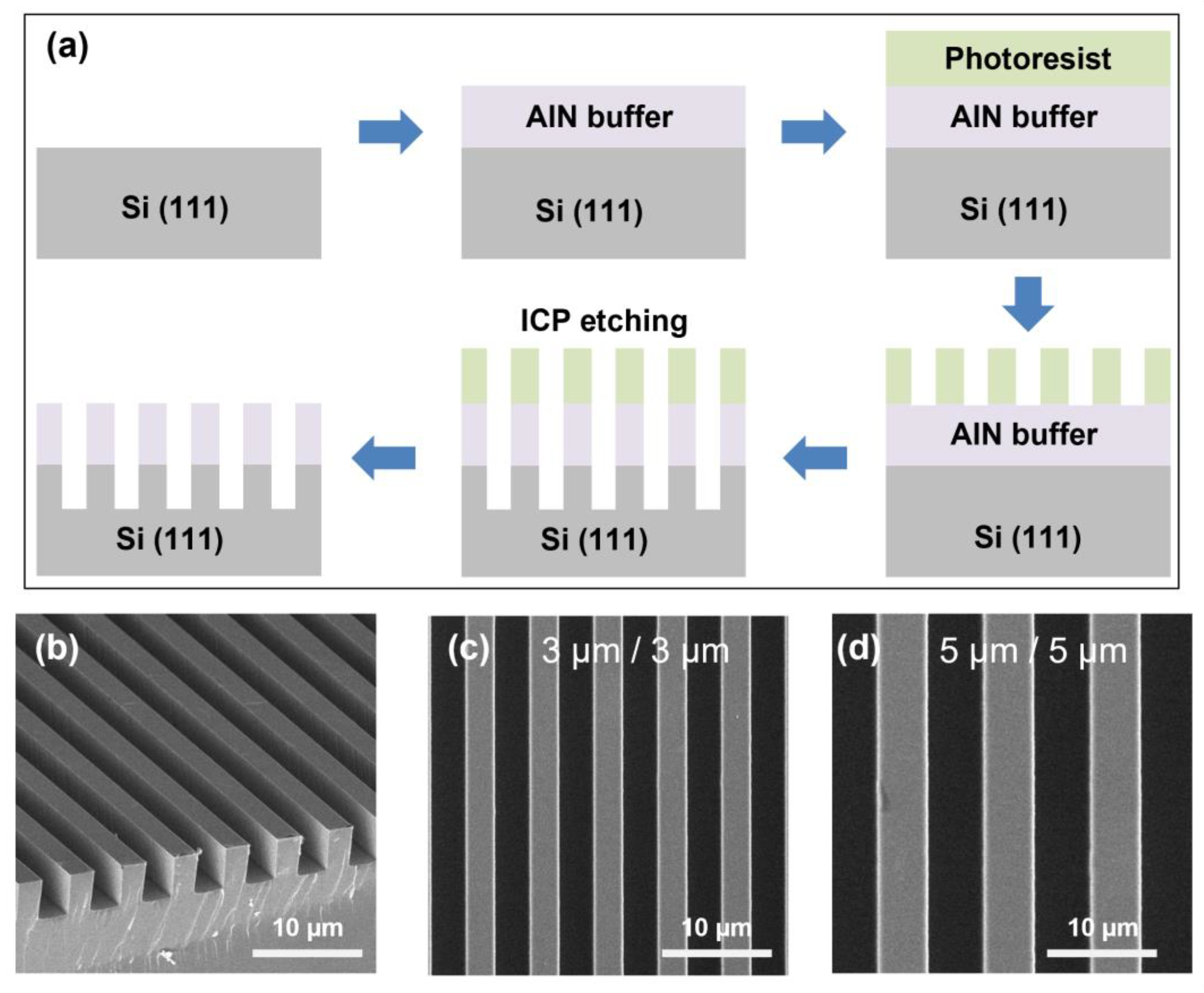
The ELO–AlN samples were grown on a Si(111) substrate by an AIXTRON close-coupled-showerhead metalorganic chemical-vapor-deposition reactor. Trimethylaluminum and ammonia were used as precursors for aluminum and nitrogen, respectively. Firstly, a 200-nanometer-thick AlN buffer layer was grown on the Si substrate. The growth temperature and V/III ratio were 1200 °C and 4000, respectively. The AlN templates were then removed from the reactor and patterned into period stripes by conventional lithography and inductively coupled plasma etching. For template A, 5-micrometer-depth stripes with a nominally 3-micrometer-width ridge/trench (6-micrometer period) were defined along the AlN <10> direction. The reason why the stripe direction was defined along the AlN<10> direction was to encourage the coalescence of ELO and AlN, since AlN is likely to grow laterally along the AlN<11> direction [23]. For template B, the width of ridge and trench were changed to 5 μm with the same strip directions. The schematic fabrication steps for the AlN/Si template are shown in Figure 1a. The perspective and plan views from the scanning electron microscope (SEM) for template A are shown in Figure 1b,c, respectively. The plan view of SEM for template B is shown in Figure 1d.
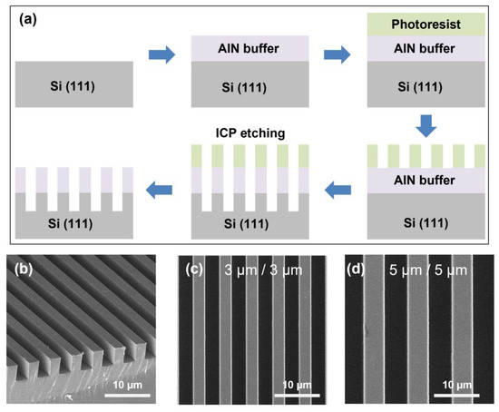
Figure 1.
(a) The fabrication process for the stripe-patterned AlN/Si templates. (b) The SEM perspective-view image for template A. The SEM plan-view images for (c) template A and (d) template B.
Subsequently, both templates A and B were loaded back into the reactor together to regrow 5.8-micrometer-thick AlN film. The regrown samples designed to be 3 μm and 5 μm wide were labeled as sample A and sample B, respectively. Therefore, the total thicknesses of AlN epilayers for both samples were 6 μm. The growth temperature and V/III ratio during the ELO were 1360 °C and 40, respectively, to encourage the lateral growth of AlN by enhancing the Al adatom migration [32,33]. In order to study the coalescence process of ELO–AlN, a control sample (named sample B1) with a regrown AlN thickness of only 3 μm was also grown on another AlN template B.
The surface morphologies of samples were studied by SEM (FEI Quanta 400 FEG) and atomic-force microscopy (AFM, Bruker Dimension Icon). The FWHM values of the X-ray-diffraction scan’s rocking curves were measured by high-resolution XRD (Bruker D8 Discover). The Raman spectra were collected by Horriba-JY LABRAM HR confocal micro-Raman system with 532-nanometer laser. Cross-sectional high-angle annular dark-field (HAADF) scanning transmission electron microscopy (STEM) images and weak-beam transmission electron microscopy (TEM) images were recorded using a 200-kilovolt Talos F200X STEM. The TEM samples were prepared by focused-ion-beam milling. Before milling, 20 nm Au, 20 nm carbon, and 300 nm Pt were deposited on the surfaces of samples in order to improve the conductivity of the material, as well as to prevent surface damage induced by ion beam. The cathodoluminescence (CL) image and spectra were recorded under 10 kV using a Gatan MonoCL3+ system at room temperature.
3. Results and Discussion
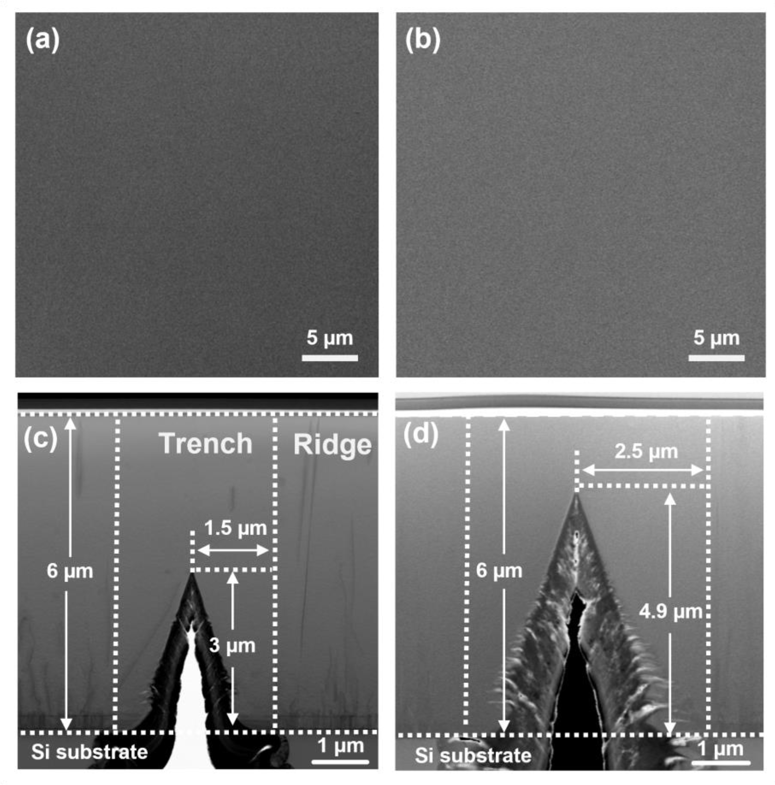
Figure 2a,b shows the SEM micrographs of samples A and B, respectively. The smooth surfaces without noticeable cracks and stripe patterns of both samples indicate that the ELO–AlN layer was fully coalesced. The cross-sectional STEM images provide further information on the coalescence behavior. As shown in Figure 2c, the vertical regrowth of the ELO–AlN for sample A was 2.8 μm when the coalescence is completed, while the lateral growth width was only 1.5 μm. This corresponded to a lateral-to-vertical-growth ratio (LTVGR) of around 1:1.86. For sample B, with a larger strip pattern (5-micrometer period), the ELO–AlN reached complete coalescence after 4.7 μm of vertical growth and 2.5 μm of lateral growth, as shown in Figure 2d, which gives a LTVGR of around 1:1.88, indicating a significantly faster lateral growth rate than that in previous reports [23,24,25,26,30]. The quick coalescence can be attributed to the high growth temperature (1360 °C) and ultralow V/III ratio (40), which enhanced the Al adatom migration [34]. It was noticed that air voids were formed in the trench areas during the AlN–ELO as shown in the cross-sectional STEM. These voids play a key role in the relaxation of tensile stress to suppress crack formation and reduce the TDD of top AlN.

Figure 2.
The SEM plan-view images for (a) sample A and (b) sample B. Cross-sectional STEM images for (c) sample A and (d) sample B.
To study the coalescence process of the AlN–ELO, a cross-sectional SEM was performed for the control sample B1, which was not fully coalesced, as shown in Figure 3a. This revealed an interesting feature of the ELO’s coalescence: two asymmetrical facets were formed during the AlN’s lateral growth. The upper facet had an angle of with respect to the c-plane, corresponding to the AlN {11} plane. The bottom facet had an angle of with respect to the c-plane, corresponding to the AlN {11} plane.
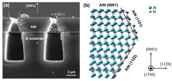
Figure 3.
(a) Cross-sectional SEM image of sample B1. (b) Schematic diagram of the atomic configuration for wurtzite ELO–AlN film grown on Si showing the preferred facets of the AlN {11} and AlN {11} planes.
In order to explain why the two asymmetrical facets were formed, an atomic configuration of the ELO–AlN over the trench area was modeled, and it is shown in Figure 3b. The {11} facet, which corresponded to the +c direction, was mixed with Al and N termination. It appears that the Al atoms exhibited only one dangling bond, while the N atoms exhibited two dangling bonds, corresponding to an Al–N dangling-bond ratio of 0.5. However, the {11} facet had an Al–N dangling-bond ratio equal to 2, which was much higher than that of the {11} facet. We conclude that the crystallographic surfaces with a low Al–N dangling bond ratio tended to be more stable during the ELO under ultra-low V/III (Ga-rich conditions) [35], which would explain the asymmetrical facets shown in Figure 3a. Moreover, in view of growth kinetics, the growth velocity of the {11} plane was higher than that of the {11} plane, as evidenced by the kinetic Wulff plots [36]. Therefore, the lateral growth and coalescence was dominated by the AlN {11} plane and the AlN (0001) plane until the ELO and AlN merged.
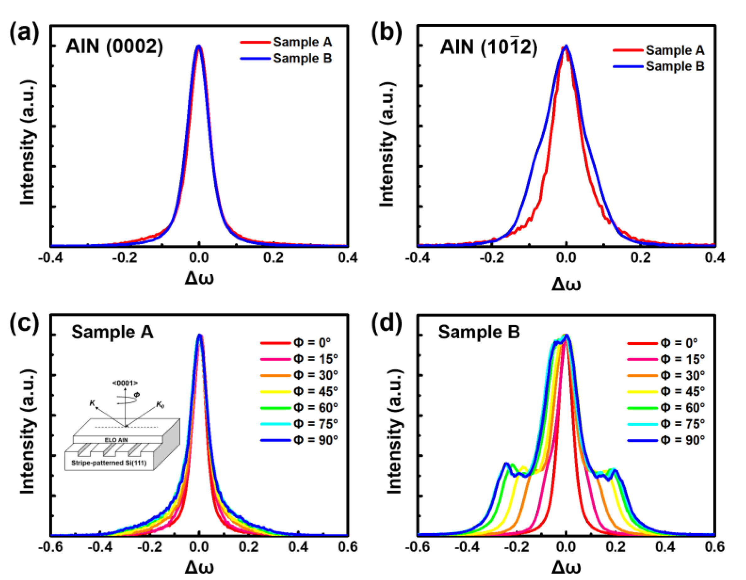
Figure 4 shows the XRD measurements for samples A and B. For sample B, with a 5-micrometer-wide trench, the FWHM values of the XRD rocking curves for the AlN (0002) and (10) planes were 272 and 533 arcsec, respectively. For sample A, with a narrowed trench width of 3 μm, the FWHM values of the AlN (0002) and (10) planes were largely reduced to 260 and 374 arcsec, respectively. The TDD of the ELO–AlN films can be estimated using the classical formulas below [37].
where the and are the FWHM values of the (0002) and (10) planes, respectively. The and are the Burgers vectors of the c-type and a-type TDs, respectively, and the magnitude of the Burgers vectors for the a-type TDs is equal to the lattice parameter (a = 0.3112 nm) along the <11–20> a-axis, while the magnitude of the Burgers vectors for the c-type TDs is equal to the lattice parameter (c = 0.4980 nm) along the <0001> c-axis. The is the lattice plane’s inclination angle ( = 42.757°). The calculated screw- and edge-type dislocation densities for sample A were 1.4 × 108 cm−2 and 1.2 × 109 cm−2, respectively, corresponding to a total TDD of 1.3 × 109 cm−2. It is worth noting that the TDD of the ELO–AlN grown on the Si for sample A was lower than the previously reported values, as shown in Table 1.
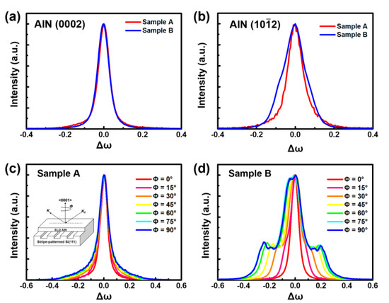
Figure 4.
The typical XRD rocking curves of (a) AlN (0002) plane and (b) AlN (10) plane for samples A and B. The Φ-scan-dependent XRD rocking curves of the AlN (0002) plane for (c) sample A and (d) sample B. The inset is the schematic diagram illustrating the rotation angle Φ. The K is the scattering vector.

Table 1.
The thickness and XRD FWHM of the ELO–AlN film grown on patterned Si substrates reported in the past few years.
In order to further study the crystalline quality of the two samples, the XRD rocking curves of the AlN (0002) were examined along with the increase in the Φ angle every 15 degrees. The Φ angle is defined as the angle between the X-ray-diffraction plane and the stripe direction, as shown in the inset of Figure 4c. For sample A, the rocking curves of the AlN (0002) scans showed a slight broadening of 56 arcsec, revealing a negligible wing-tilt angle. In stark contrast, the rocking curves for sample B presented major broadening, along with several satellite peaks as the Φ angle increased, indicating a large wing tilt of 0.44° in the coalescence area of the ELO–AlN with 5-micrometer-wide trenches. The wing tilt is believed to be the primary origin of the high-density TDD during coalescence, which degrades the crystalline quality of ELO–AlN [34,38,39].
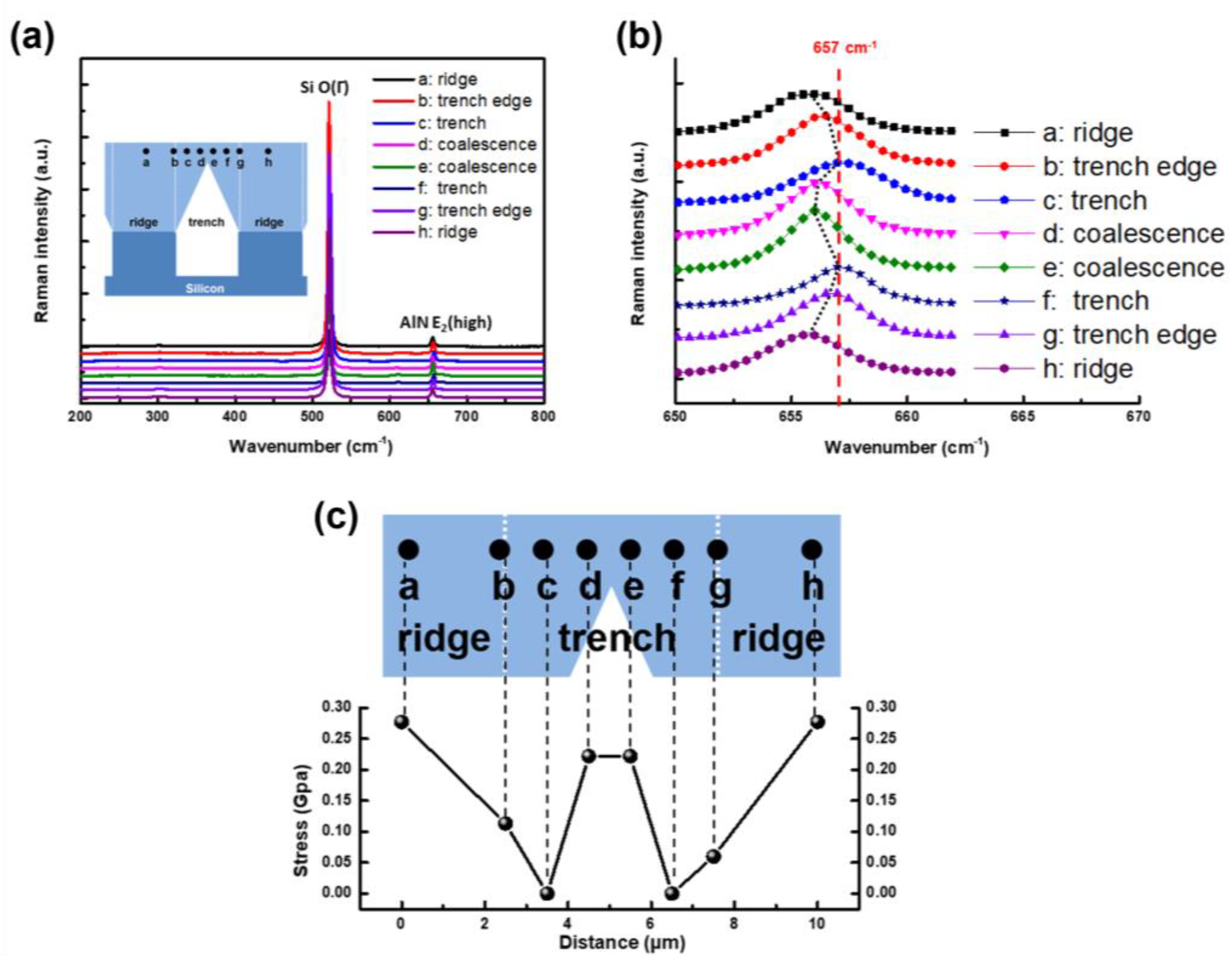
Micro-Raman spectra were then performed for sample B from the surface along the AlN [11] direction to study the origin of the wing tilt in the ELO–AlN, as shown in Figure 5. It was observed that only the Si O(Γ) and AlN E2(h) peaks appeared in the Raman spectra, as shown in Figure 5a. Detailed Raman shifts of the AlN E2(h) along the trench/ridge can be found in Figure 5b. It is worth mentioning that the Raman spectra were calibrated by aligning the Si O(Γ) peaks before analyzing the E2(h) peak positions of the AlN. In fact, the E2(h) shift of AlN is sensitive to the biaxial strain along the c-plane of AlN, which is often used to evaluate the stress in AlN films [16]. Obviously, most of the AlN E2(h) peaks shifted to low wavenumbers compared to those of the bulk AlN value of 657 cm−1, indicating residual tensile stress in the ELO–AlN film. The shift in the AlN E2(h) peak varied along the AlN direction from the ridge to the trench area, demonstrating a non-homogenous strain across the trench region. According to the relationship between the residual stress (σ) and the Raman shift (Δω) of E2(h),
where the value of the stress coefficient K is 4.5 cm−1 GPa−1 for the AlN films grown on the Si [3]. The stress across the trench region can therefore be calculated as shown in Figure 5c. As the tests moved from the ridge center (Position a/h) to the trench center (Position c/f), the thickness of the AlN gradually decreased, with the tensile stress gradually decreasing from 0.27 GPa to almost zero [40]. However, it is worth noting that the residual tensile stress dramatically increased to 0.23 GPa in the coalescence region (Position d/e), further revealing a large wing tilt in sample B. Since the residual stress results from the mismatch in the thermal expansion coefficient and crystal lattice between AlN and Si [41,42,43], the increase in the vertical growth thickness increased the tensile stress in the ELO–AlN films. Therefore, for sample B, with a larger trench width of 5 μm, a longer vertical growth time with a greater thickness would arise before the ELO–AlN coalescence, leading to greater tensile stress and, therefore, a significant wing tilt. Therefore, it can be further concluded that the better crystal quality of sample A (with a narrow trench width of 3 μm) resulted from a smaller wing-tilt angle in the trench area of the ELO–AlN. It is worth highlighting that the tensile stress of the ELO–AlN samples in this work was within 0.27 GPa, which was much lower than the other reported value of 1 GPa for the AlN on Si. The low tensile stress of our ELO–AlN on Si can be attributed to the formation of air voids, which helps to increase the thickness of crack-free AlN and to reduce the TDD.
(Δω) = K · σ
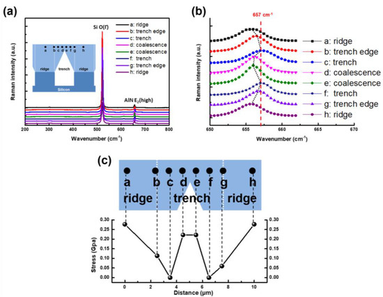
Figure 5.
(a) Surface Raman spectra and (b) details of peak shift of AlN E2(h) mode from ridge to trench areas of sample B. (c) Residual stress as a function of the distance from ridge center of sample B.
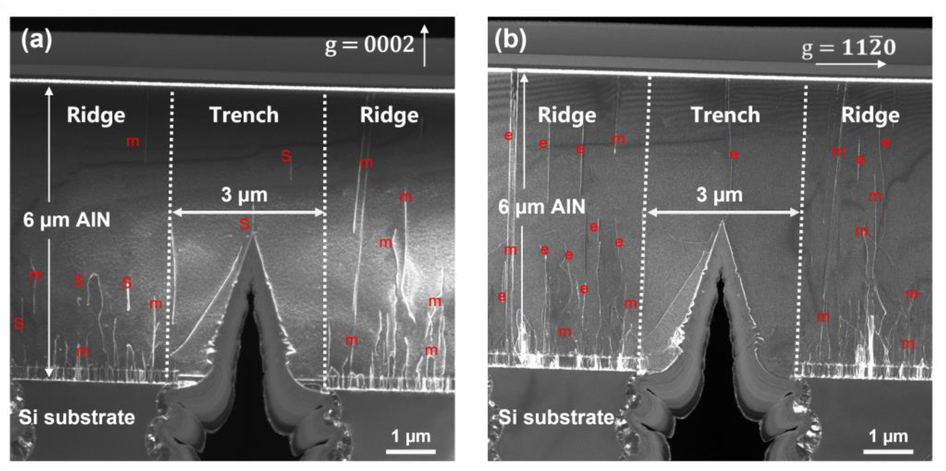
The TEM characterization for sample A, which had better crystal quality, was taken to study the dislocation evolution in the ELO–AlN film. Figure 6a,b shows the weak-beam dark-field TEM images with g = 0002 and g = 11, respectively. In the ridge area, a high TDD at the AlN/Si interface caused by the lattice mismatch can be clearly observed. Next, the TDs bent and were annihilated with each other within about 2 μm of thickness. Furthermore, TD bending induced by the lateral growth facet was also found. Moreover, there were only a few newly generated TDs at the coalescence interface due to the small wing tilt (less than 0.2°, as discussed above) between the two adjacent islands.
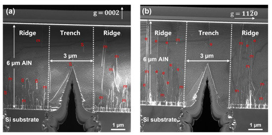
Figure 6.
Cross-sectional TEM images of sample A taken with the diffraction vectors of (a) g = 0002 and (b) g = .
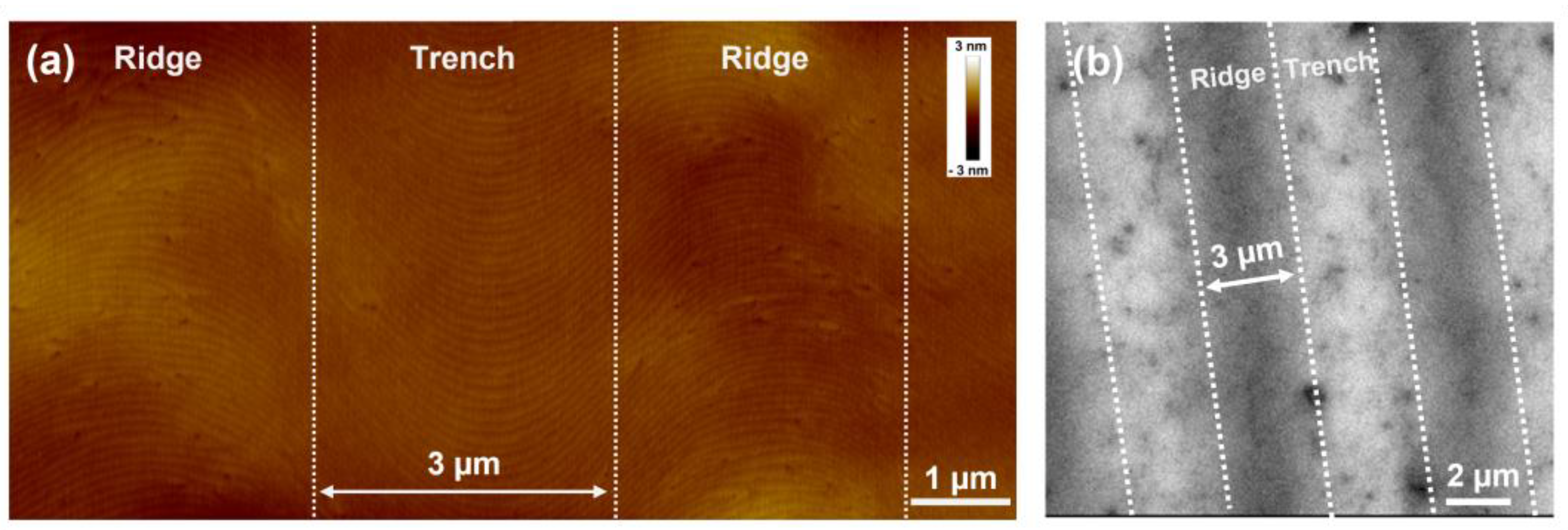
The surface morphology and TD distribution on the coalesced AlN surface of sample A was further investigated by AFM and CL measurement. As shown in Figure 7a, the coalesced ELO–AlN surface presented well-ordered atomic steps on the AFM scan, and the root-mean-square roughness was only 0.18 nm. Moreover, the density of the TDs that pinned the atom steps was about 3 × 108 cm−2, which was much lower than that obtained from the XRD results. One of the plausible reasons for this is that the XRD rocking curve was broadened by the tilt and twist between the adjacent ELO–AlN. Figure 7b shows the panchromatic CL images of sample A. The CL image presented obvious bright and dark stripes, which were correlated with the trench and ridge areas, respectively. The AlN over the trench area had a stronger CL luminescence than the ridge area, indicating a better AlN quality at the trench area. Typically, the dark spots, which represented low CL intensity, were due to the non-radiative TD defects. It is obvious that the dark spots in the ridge area gathered, almost forming a dark band, while the trench area had only a few scattered dark spots, indicating that the AlN over the trench area had a lower TDD than the ridge area, which was consistent with the TEM and AFM results.

Figure 7.
(a) AFM image and (b) CL image of sample A with 3-micrometer-wide trench/ridge.
4. Conclusions
In conclusion, the ELO of the high-quality AlN on the stripe-patterned Si(111) substrate with two trench widths, of 3 μm and 5 μm, was studied. The LTVGRs for the samples patterned with 3-micrometer- and 5-micrometer-wide trenches were 1:1.86 and 1:1.88, respectively, indicating a significantly faster lateral growth rate. The two asymmetrical facets of the AlN (11) and AlN (11) planes were formed during the lateral growth, and the lateral growth and coalescence were finally dominated by the AlN {11} plane and the AlN (0001) plane during the ELO–AlN merger. By narrowing down the stripe width from 5 μm to 3 μm, the vertical growth thickness before the AlN coalescence was reduced from 4.7 μm to 2.8 μm, resulting in a large decrease in the internal tensile stress and tilt angle, thereby contributing to the formation of crack-free, 6-micrometer-thick, high-quality AlN films on the Si substrates. The FWHMs of the XRD curves were as low as 260 and 374 arcsec for the AlN (0002) and (10) planes, respectively, corresponding to a record-low TDD of 1.3 × 109 cm−2. This work paves the way for the fabrication of high-performance Al(Ga)N-based thin-film devices, such as UV LEDs and AlN bulk acoustic resonators grown on Si.
Author Contributions
Conceptualization, Y.H. and J.L.; methodology, Y.H. and X.S.; validation, Y.H., X.Z. and M.F.; formal analysis, Y.H., J.L. and Q.S.; investigation, Y.H., H.G. and Y.Z.; resources, Q.S.; writing—original draft preparation, Y.H.; writing—review and editing, Y.H. and J.L.; visualization, Y.H. and X.Z.; supervision, J.L. and Q.S.; project administration, J.L. and Q.S.; funding acquisition, Q.S. and H.Y. All authors have read and agreed to the published version of the manuscript.
Funding
This research was funded by National Key R&D Program of China (grant nos. 2022YFB3604300, 2022YFB3604800, 2021YFB3601600, and 2022YFB2802801); Guangdong Province Key-Area R&D Program (grant nos. 2019B090917005, 2020B010174004, 2019B090904002, and 2019B090909004); Natural Science Foundation of China (grant nos. 62274177, 62174174, 62074158, 62275263, and 61874131); Jiangxi Double Thousand Plan (grant no. S2018CQKJ0072); Jiangxi Science and Technology Program (grant no. 20212BDH80026); Strategic Priority Research Program of CAS (grant nos. XDB43000000 and XDB43020200); Key Research Program of Frontier Sciences, CAS (grant nos. QYZDB-SSW-JSC014 and ZDBS-LY-JSC040); Bureau of International Cooperation, CAS (grant no. 121E32KYSB20210002); Key R&D Program of Jiangsu Province (grant nos. BE2021051 and BE2020004-2); and Suzhou Science and Technology Program (grant nos. SJC2021002 and SYC2022089).
Data Availability Statement
The data that support the findings of this study are available from the corresponding author upon reasonable request.
Acknowledgments
We are thankful for the technical support from Nano Fabrication Facility, Platform for Characterization and Test, and Nano-X of SINANO, CAS.
Conflicts of Interest
The authors declare no conflict of interest.
References
- Kneissl, M.; Seong, T.-Y.; Han, J.; Amano, H. The emergence and prospects of deep-ultraviolet light-emitting diode technologies. Nat. Photonics 2019, 13, 233. [Google Scholar] [CrossRef]
- Liu, Y.; Cai, Y.; Zhang, Y.; Tovstopyat, A.; Liu, S.; Sun, C. Materials, Design, and Characteristics of Bulk Acoustic Wave Resonator: A Review. Micromachines 2020, 11, 630. [Google Scholar] [CrossRef] [PubMed]
- Dai, Y.; Li, S.; Sun, Q.; Peng, Q.; Gui, C.; Zhou, Y.; Liu, S. Properties of AlN film grown on Si(111). J. Cryst. Growth 2016, 435, 76. [Google Scholar] [CrossRef]
- Zhao, W.; Asadi, M.J.; Li, L.; Chaudhuri, R.; Nomoto, K.; Xing, H.G.; Hwang, J.C.M.; Jena, D. X-band epi-BAW resonators. J. Appl. Phys. 2022, 132, 024503. [Google Scholar] [CrossRef]
- Zhang, Y.; Long, H.; Zhang, J.; Tan, B.; Chen, Q.; Zhang, S.; Shan, M.; Zheng, Z.; Dai, J.; Chen, C. Fast growth of high quality AlN films on sapphire using a dislocation filtering layer for ultraviolet light-emitting diodes. Crystengcomm 2019, 21, 4072. [Google Scholar] [CrossRef]
- Ezubchenko, I.S.; Chernykh, M.Y.; Mayboroda, I.O.; Trun’kin, I.N.; Chernykh, I.A.; Zanaveskin, M.L. High-Quality AlN Layers Grown on Si(111) Substrates by Metalorganic Chemical Vapor Deposition. Crystallogr. Rep. 2020, 65, 122. [Google Scholar] [CrossRef]
- Huang, L.; Li, Y.; Wang, W.; Li, X.; Zheng, Y.; Wang, H.; Zhang, Z.; Li, G. Growth of high-quality AlN epitaxial film by optimizing the Si substrate surface. Appl. Surf. Sci. 2018, 435, 163. [Google Scholar] [CrossRef]
- Tao, T.; Zhang, R.; Zhi, T.; Liu, B.; Lei, J.; Dai, J.; Xie, Z.; Zhou, Y.; Chen, D.; Lu, H. Observation and Modeling of Leakage Current in AlGaN Ultraviolet Light Emitting Diodes. IEEE Photonics Technol. Lett. 2019, 31, 1697. [Google Scholar] [CrossRef]
- Huang, Y.; Liu, J.; Sun, X.; Zhan, X.; Sun, Q.; Gao, H.; Feng, M.; Zhou, Y.; Ikeda, M.; Yang, H. Crack-free high quality 2 μm-thick Al0.5Ga0.5N grown on a Si substrate with a superlattice transition layer. Crystengcomm 2020, 22, 1160. [Google Scholar] [CrossRef]
- Li, Z.; Liu, L.; Huang, Y.; Sun, Q.; Feng, M.; Zhou, Y.; Zhao, H.; Yang, H. High-power AlGaN-based near-ultraviolet light-emitting diodes grown on Si(111). Appl. Phys. Express 2017, 10, 072101. [Google Scholar] [CrossRef]
- SaifAddin, B.K.; Almogbel, A.; Zollner, C.J.; Foronda, H.; Alyamani, A.; Albadri, A.; Iza, M.; Nakamura, S.; DenBaars, S.P.; Speck, J.S. Fabrication technology for high light-extraction ultraviolet thin-film flip-chip (UV TFFC) LEDs grown on SiC. Semicond. Sci. Technol. 2019, 34, 035007. [Google Scholar] [CrossRef]
- Takeuchi, M.; Maegawa, T.; Shimizu, H.; Ooishi, S.; Ohtsuka, T.; Aoyagi, Y. AlN/AlGaN short-period superlattice sacrificial layers in laser lift-off for vertical-type AlGaN-based deep ultraviolet light emitting diodes. Appl. Phys. Lett. 2009, 94, 061117. [Google Scholar] [CrossRef]
- Cho, H.K.; Krüger, O.; Külberg, A.; Rass, J.; Zeimer, U.; Kolbe, T.; Knauer, A.; Einfeldt, S.; Weyers, M.; Kneissl, M. Chip design for thin-film deep ultraviolet LEDs fabricated by laser lift-off of the sapphire substrate. Semicond. Sci. Technol. 2017, 32, 12LT01. [Google Scholar] [CrossRef]
- Sun, Y.; Zhou, K.; Feng, M.; Li, Z.; Zhou, Y.; Sun, Q.; Liu, J.; Zhang, L.; Li, D.; Sun, X.; et al. Room-temperature continuous-wave electrically pumped InGaN/GaN quantum well blue laser diode directly grown on Si. Light Sci. Appl. 2018, 7, 13. [Google Scholar] [CrossRef]
- Feng, M.; Wang, J.; Zhou, R.; Sun, Q.; Gao, H.; Zhou, Y.; Liu, J.; Huang, Y.; Zhang, S.; Ikeda, M.; et al. On-Chip Integration of GaN-Based Laser, Modulator, and Photodetector Grown on Si. IEEE J. Sel. Top. Quantum Electron. 2018, 24, 1. [Google Scholar] [CrossRef]
- Liu, J.; Huang, Y.; Sun, X.; Zhan, X.; Sun, Q.; Gao, H.; Feng, M.; Zhou, Y.; Ikeda, M.; Yang, H. Wafer-scale crack-free 10 µm-thick GaN with a dislocation density of 5.8 × 107 cm−2 grown on Si. J. Phys. D 2019, 52, 425102. [Google Scholar] [CrossRef]
- Sun, Q.; Yan, W.; Feng, M.; Li, Z.; Feng, B.; Zhao, H.; Yang, H. GaN-on-Si blue/white LEDs: Epitaxy, chip, and package. J. Semicond. 2016, 37, 044006. [Google Scholar] [CrossRef]
- Sun, Y.; Zhou, K.; Sun, Q.; Liu, J.; Feng, M.; Li, Z.; Zhou, Y.; Zhang, L.; Li, D.; Zhang, S.; et al. Room-temperature continuous-wave electrically injected InGaN-based laser directly grown on Si. Nat. Photonics 2016, 10, 595. [Google Scholar] [CrossRef]
- Zhang, Z.-Z.; Yang, J.; Zhao, D.-G.; Liang, F.; Chen, P.; Liu, Z.-S. Influence of the lattice parameter of the AlN buffer layer on the stress state of GaN film grown on (111) Si. Chin. Phys. B 2023, 32, 028101. [Google Scholar] [CrossRef]
- Bardhan, A.; Raghavan, S. Growth design for high quality AlxGa(1−x)N layer with high AlN-fraction on Si (1 1 1) substrate by MOCVD. J. Cryst. Growth 2022, 578, 126418. [Google Scholar] [CrossRef]
- Lange, A.P.; Mahajan, S. Influence of trimethylaluminum predoses on the growth morphology, film-substrate interface, and microstructure of MOCVD-grown AlN on (1 1 1)Si. J. Cryst. Growth 2019, 511, 106. [Google Scholar] [CrossRef]
- Radtke, G.; Couillard, M.; Botton, G.A.; Zhu, D.; Humphreys, C.J. Structure and chemistry of the Si(111)/AlN interface. Appl. Phys. Lett. 2012, 100, 011910. [Google Scholar] [CrossRef]
- Mino, T.; Hirayama, H.; Takano, T.; Tsubaki, K.; Sugiyama, M. Realization of 256–278 nm AlGaN-Based Deep-Ultraviolet Light-Emitting Diodes on Si Substrates Using Epitaxial Lateral Overgrowth AlN Templates. Appl. Phys. Express 2011, 4, 092104. [Google Scholar] [CrossRef]
- Cho, C.-Y.; Zhang, Y.; Cicek, E.; Rahnema, B.; Bai, Y.; McClintock, R.; Razeghi, M. Surface plasmon enhanced light emission from AlGaN-based ultraviolet light-emitting diodes grown on Si(111). Appl. Phys. Lett. 2013, 102, 211110. [Google Scholar] [CrossRef]
- Cicek, E.; McClintock, R.; Cho, C.Y.; Rahnema, B.; Razeghi, M. AlxGa1−xN-based solar-blind ultraviolet photodetector based on lateral epitaxial overgrowth of AlN on Si substrate. Appl. Phys. Lett. 2013, 103, 181113. [Google Scholar] [CrossRef]
- Zhang, Y.; Gautier, S.; Cho, C.-Y.; Cicek, E.; Vashaei, Z.; McClintock, R.; Bayram, C.; Bai, Y.; Razeghi, M. Near milliwatt power AlGaN-based ultraviolet light emitting diodes based on lateral epitaxial overgrowth of AlN on Si(111). Appl. Phys. Lett. 2013, 102, 011106. [Google Scholar] [CrossRef]
- Tran, B.T.; Hirayama, H.; Maeda, N.; Jo, M.; Toyoda, S.; Kamata, N. Direct Growth and Controlled Coalescence of Thick AlN Template on Micro-circle Patterned Si Substrate. Sci. Rep. 2015, 5, 14734. [Google Scholar] [CrossRef]
- Demir, İ.; Robin, Y.; McClintock, R.; Elagoz, S.; Zekentes, K.; Razeghi, M. Direct growth of thick AlN layers on nanopatterned Si substrates by cantilever epitaxy. Phys. Status Solidi (A) 2017, 214, 1600363. [Google Scholar] [CrossRef]
- Tran, B.T.; Hirayama, H. Growth and Fabrication of High External Quantum Efficiency AlGaN-Based Deep Ultraviolet Light-Emitting Diode Grown on Pattern Si Substrate. Sci. Rep. 2017, 7, 12176. [Google Scholar] [CrossRef] [PubMed]
- Robin, Y.; Ding, K.; Demir, I.; McClintock, R.; Elagoz, S.; Razeghi, M. High brightness ultraviolet light-emitting diodes grown on patterned silicon substrate. Mater. Sci. Semicond. Process. 2019, 90, 87. [Google Scholar] [CrossRef]
- Shen, J.; Yang, X.; Liu, D.; Cai, Z.; Wei, L.; Xie, N.; Xu, F.; Tang, N.; Wang, X.; Ge, W.; et al. High quality AlN film grown on a nano-concave-circle patterned Si substrate with an AlN seed layer. Appl. Phys. Lett. 2020, 117, 022103. [Google Scholar] [CrossRef]
- Roskowski, A.; Preble, E.; Einfeldt, S.; Miraglia, P.; Davis, R. Maskless pendeo-epitaxial growth of GaN films. J. Electron. Mater. 2002, 31, 421. [Google Scholar] [CrossRef]
- Hirayama, H.; Fujikawa, S.; Norimatsu, J.; Takano, T.; Tsubaki, K.; Kamata, N. Fabrication of a low threading dislocation density ELO-AlN template for application to deep-UV LEDs. Phys. Status Solidi (C) 2009, 6, S356–S359. [Google Scholar] [CrossRef]
- Chen, X.; Yan, J.; Zhang, Y.; Tian, Y.; Guo, Y.; Zhang, S.; Wei, T.; Wang, J.; Li, J. Improved Crystalline Quality of AlN by Epitaxial Lateral Overgrowth Using Two-Phase Growth Method for Deep-Ultraviolet Stimulated Emission. IEEE Photonics J. 2016, 8, 2300211. [Google Scholar] [CrossRef]
- Founta, S.; Bougerol, C.; Mariette, H.; Daudin, B.; Vennéguès, P. Anisotropic morphology of nonpolar a-plane GaN quantum dots and quantum wells. J. Appl. Phys. 2007, 102, 2300211. [Google Scholar] [CrossRef]
- Sun, Q.; Yerino, C.D.; Leung, B.; Han, J.; Coltrin, M.E. Understanding and controlling heteroepitaxy with the kinetic Wulff plot: A case study with GaN. J. Appl. Phys. 2011, 110, 053517. [Google Scholar] [CrossRef]
- Lee, S.R.; West, A.M.; Allerman, A.A.; Waldrip, K.E.; Follstaedt, D.M.; Provencio, P.P.; Koleske, D.D.; Abernathy, C.R. Effect of threading dislocations on the Bragg peakwidths of GaN, AlGaN, and AlN heterolayers. Appl. Phys. Lett. 2005, 86, 241904. [Google Scholar] [CrossRef]
- Hagedorn, S.; Knauer, A.; Mogilatenko, A.; Richter, E.; Weyers, M. AlN growth on nano-patterned sapphire: A route for cost efficient pseudo substrates for deep UV LEDs. Phys. Status Solidi (A) 2016, 213, 3178. [Google Scholar] [CrossRef]
- Mogilatenko, A.; Küller, V.; Knauer, A.; Jeschke, J.; Zeimer, U.; Weyers, M.; Tränkle, G. Defect analysis in AlGaN layers on AlN templates obtained by epitaxial lateral overgrowth. J. Cryst. Growth 2014, 402, 222. [Google Scholar] [CrossRef]
- Pantha, B.N.; Dahal, R.; Nakarmi, M.L.; Nepal, N.; Li, J.; Lin, J.Y.; Jiang, H.X.; Paduano, Q.S.; Weyburne, D. Correlation between optoelectronic and structural properties and epilayer thickness of AlN. Appl. Phys. Lett. 2007, 90, 241101. [Google Scholar] [CrossRef]
- Yu, N.S.; Zhu, X.L.; Peng, M.Z.; Zhou, J.M. Wing tilt investigations on GaN epilayer grown on maskless grooved sapphire by MOCVD. J. Mater. Sci. 2009, 45, 1503. [Google Scholar] [CrossRef]
- Barabash, R.I.; Roder, C.; Ice, G.E.; Einfeldt, S.; Budai, J.D.; Barabash, O.M.; Figge, S.; Hommel, D. Spatially resolved distribution of dislocations and crystallographic tilts in GaN layers grown on Si(111) substrates by maskless cantilever epitaxy. J. Appl. Phys. 2006, 100, 053103. [Google Scholar] [CrossRef]
- Benyoucef, M.; Kuball, M.; Beaumont, B.; Gibart, P. Raman mapping, photoluminescence investigations, and finite element analysis of epitaxial lateral overgrown GaN on silicon substrates. Appl. Phys. Lett. 2002, 80, 2275. [Google Scholar] [CrossRef]
Disclaimer/Publisher’s Note: The statements, opinions and data contained in all publications are solely those of the individual author(s) and contributor(s) and not of MDPI and/or the editor(s). MDPI and/or the editor(s) disclaim responsibility for any injury to people or property resulting from any ideas, methods, instructions or products referred to in the content. |
© 2023 by the authors. Licensee MDPI, Basel, Switzerland. This article is an open access article distributed under the terms and conditions of the Creative Commons Attribution (CC BY) license (https://creativecommons.org/licenses/by/4.0/).

