Article

High-Performance and Flexible Metamaterial Wave Absorbers with Specific Bandwidths for the Microwave Device

1
Department of Physics, Hanyang University, Seoul 04763, Republic of Korea
2
Alpha ADT Co., Hwaseong 18469, Republic of Korea
3
Department of Optical Science and Engineering, Fudan University, Shanghai 200433, China
*
Author to whom correspondence should be addressed.
Crystals 2023, 13(6), 868; https://doi.org/10.3390/cryst13060868
Submission received: 27 April 2023 / Revised: 22 May 2023 / Accepted: 24 May 2023 / Published: 26 May 2023
(This article belongs to the Section Crystalline Metals and Alloys)

Abstract

:
In this paper, we proposed a high-performance electromagnetic-wave metamaterial absorber which can be used directly for 5G technology. The absorber exhibits a high performance in a tailored frequency range of 28 ± 1 GHz. At both transverse-electric and transverse-magnetic polarization, the absorption exceeds 99% when the electromagnetic wave is incident normally, and the absorption keeps being over 97% as the incident angle increases even to 45 degrees. The absorber is flexible, and it is very suitable for mass production because the production process is simple. In addition, the minimum dimension of the meta-structure is only 0.2 mm, and the cost is relatively low. Similarly, another high-performance metamaterial absorber with a tailored bandwidth at the center frequency of 77 GHz, which is relevant to self-driving cars, was also prepared by a minimal adjustment to the original structure.

1. Introduction

Metamaterial (MM) is a kind of artificial material. Simply speaking, metamaterial is composed of dielectric material and periodically pattered metal. The propagation, absorption, and near-field properties of electromagnetic (EM) waves can be controlled well by designing the geometric parameters, such as the shape, size, periodicity of the metallic pattern, and thickness of the dielectric layer. Research on MMs began at the end of the 19th century but did not receive much attention until it was described theoretically by Veselago et al. in 1968 [1]. In 2000, Pendry [2] first proposed the method of realizing double-negative refraction (both negative permittivity and permeability), and the next year, MMs were verified experimentally by Smith et al. [3]. Since then, MMs have penetrated into many fields, such as biosensors [4,5], antennas [6,7], super lenses [8,9], slow light [10,11], meta-surfaces [12,13,14,15], absorbers [16,17,18] and so on.
Electromagnetic (EM)-wave technology has been used widely in our daily life, especially after entering the 4G and 5G era. Meanwhile, the pollution of EM waves has become more and more serious, and one of the effective ways to solve the problem is to absorb the EM wave perfectly. Fortunately, in 2008, Landy et al. [16] proposed a metamaterial (MM)-based nearly perfect EM-wave absorber, which had the advantages of subwavelength size of the unit cells and high performance. Subsequently, a large number of different types of metamaterial absorbers (MMAs) were proposed, such as multi-absorption peaks [19,20], polarization independence [21,22], coverage of wide incident angles [23,24], tunable bandwidth, etc. According to different absorption frequencies, the absorbers were proposed for sensing, thermal imaging, wireless communication and so on.
Generally speaking, absorbers based on MMs have a relatively narrow absorption bandwidth, which limits their application fields, and appropriately widening the absorption bandwidth is still a challenge. So far, various schemes have been proposed to overcome this difficulty, such as the superposition of different resonant modes [25,26], employment of resistors [27,28,29], three-dimentionalization [30,31] and multi-layer superposition [32,33]. However, the structure becomes too complicated to lead to the corresponding preparation process, and the high absorption rate cannot be achieved at some frequencies because of depression induced by the interaction among two or multi-resonance modes. In order to extend the bandwidth of absorption, other materials can be also employed, such as liquid [34,35], graphene [36,37], conductive fibers [38] and resistive sheets [39,40]. Among the literature, Kim et al.’s work [40], in which the connection of each narrow made an ultrabroad and high-absorption band, was given great attention from us.
Typically, an MMA consists of three parts: a metal-pattern layer, a dielectric layer and a continuous metallic layer. The top layer is the part we pay the most attention to; in some cases, it can be considered as a frequency-selective surface (FSS). Here, we would like to introduce a MM-based transmission-enhanced structure [41]. As far as we know, according to the Bethe theory, the transmission efficiency of a hole is quite low if the size of hole is smaller than the wavelength. However, Aydin et al. [42] proposed that the transmission can be enhanced significantly by setting an MM in front of the hole, which has been used in designing the FSS.
The high-performance MMAs we proposed in this paper have the following merits: first of all, as the incident angle changes from 0 to 45°, in both transverse-electric (TE) and transverse-magnetic (TM) mode, absorption maintains ultrahigh absorption in a tailored frequency range of 27–29 GHz, which is good for 5G communication. This frequency band is used in 5G communication. If we cover the neighboring areas of the 5G transmitter and receivers with this developed MMA, then the signal is enhanced by eliminating the spurious ones. In other words, this means the absorption exceeds 99% for the normal incidence and exceeds 97% even at an incident angle of 45°. Furthermore, it should be emphasized that the absorption bandwidth was designed to have no excessive absorption at other frequencies, which is excellent for the minimum noise for communication. Secondly, the MMAs are flexible to accommodate any shape of object body. Thirdly, by considering the practical aspect, all the dimensions of the structure are larger than or equal to 0.2 mm, and the fabrication process is simple and at a low cost. The other system for 76–78 GHz, which can be employed for self-driving-car applications, was also prepared by a minimal adjustment to the original structure for 27–29 GHz, which is another advantage of the MMA.

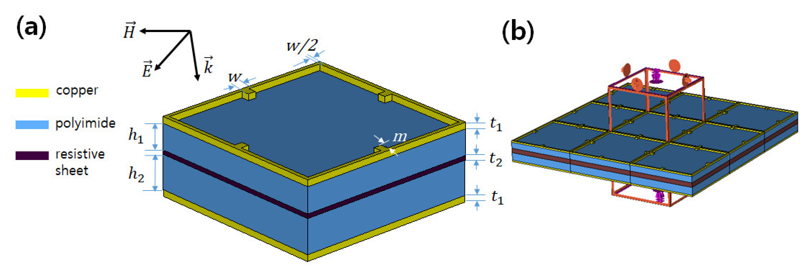
2. Materials, Structure and Methods

The MMAs are composed of 5 layers, as shown in Figure 1a, namely the copper pattern layer, the first polyimide layer, the resistive layer, the second polyimide layer and the copper continuous layer. The conductivity of copper was 5.8 × 10⁸ S/m, the resistance of the resistive sheet was 540 Ω/sq, and the dielectric constant and loss tangle of polyimide were 3.5 and 0.0027, respectively. The periodicity of structure was 4.4 mm, and the other optimized parameters are shown in Table 1.
The absorption was calculated by A = 1 R T = 1 S 11 2 S 12 2 , where R = S 11 2 and T = S 12 2 . S 11 and S12 are the reflection and transmission coefficient, respectively. Because the rear copper layer completely blocks the propagation out of the MMA, there is no transmission, and the absorption is simplified to be A = 1 S 11 2   .
The full-wave EM simulation was performed by using CST Microwave Studio software, version 5.1. The periodic boundary condition was set in the x–y plane and it was open in the z-direction, as shown in Figure 1b. We used the frequency domain solver in the simulation. The optimizing process was as follows. We fixed the resistance of the resistive sheet firstly, then after designing the structure, we checked the EM-field and surface-current distributions at the resonant frequency. Then, we tested each geometric parameter separately to obtain the influence of each on the absorption, including the shift in resonant frequency and the change of absorption. Actually, the perfect absorption in a certain situation was relatively easy to adjust, but in order to match all the conditions, we needed to really compromise among the adjustments. The equivalent-circuit theory was very useful in optimizing the structure.

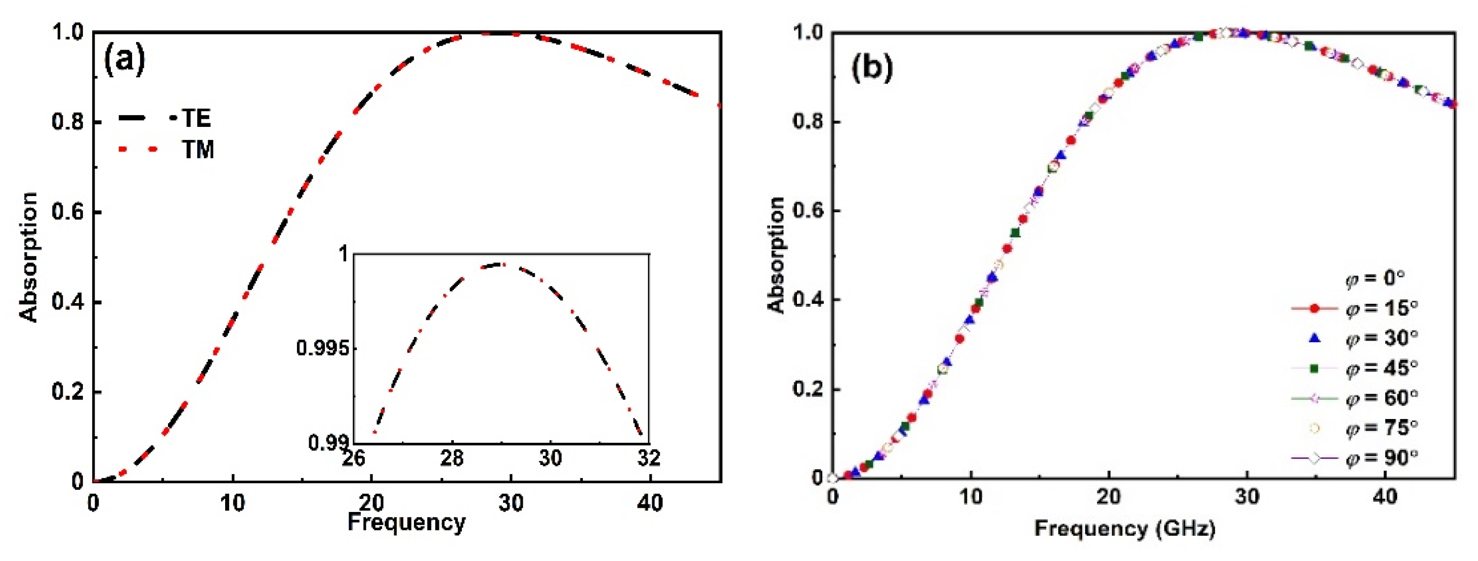
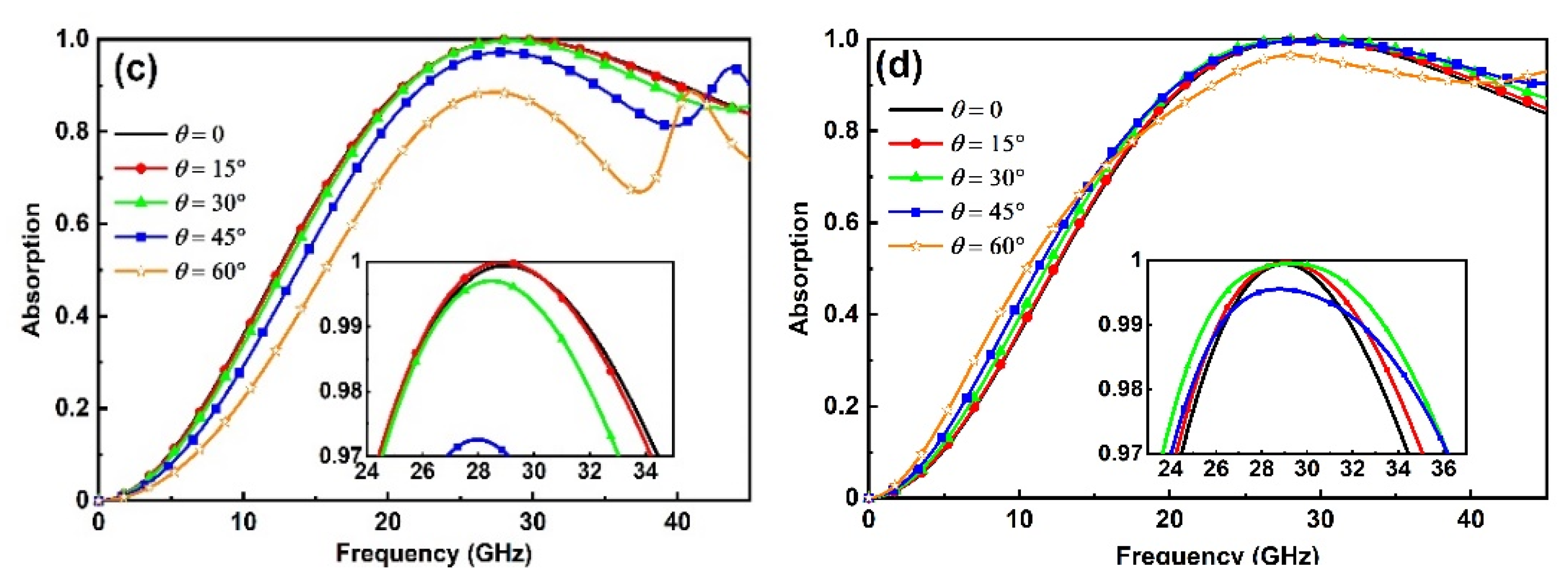
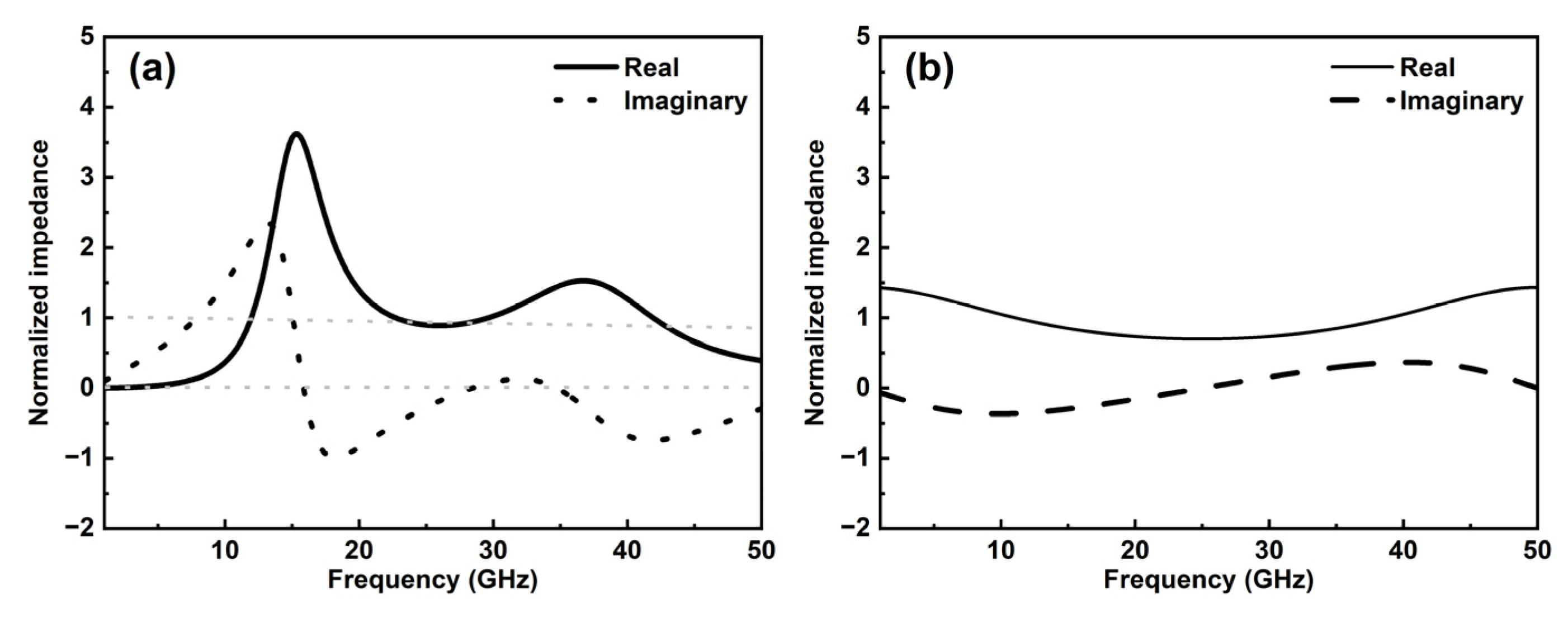
3. Results and Discussion

The simulated absorption spectra of the MMA are shown in Figure 2. Figure 2a presents the TE- and TM-polarized absorption at the normal incidence. The absorption exceeds 99% from 26.35–31.9 GHz, and at 28 GHz it reaches even 99.8%. The absorption turns out to be insensitive to the polarization angle, as shown in Figure 2b, because of the symmetry of the structure. The absorption spectra at oblique incidences are shown in Figure 2c,d. In the case of TE polarization, when the incident angle varies in a range of 0–45°, the absorption is maintained over 97% in a frequency range of 26.86–29 GHz, and it drops obviously when the angle comes to be larger than 45°. The performance in the TM mode is much better than that in TE. The absorption is more insensitive to the angle of incidence, and at frequencies of 24–36.2 GHz, the absorption is revealed to be over 97%. According to the results, the effective frequency range (EFR) is from 26.86 to 29 GHz, which satisfies the requirement for the high performance maintained in a tailored band between 27 and 29 GHz.
The effective impedance [43] of the MMA is shown in Figure 3a. Around 29 GHz, the real part of impedance is observed to be close to 1, and the imaginary part approaches 0, which means the impedance is matched nearly perfectly at that frequency. Figure 3b displays the impedance of the MMA structure without the MM pattern and polyimide-1 layer, which is used in the impedance analysis below.
The equivalent-circuit model of the structure is presented in Figure 3c. The input impedance can be expressed as follows [44,45]:
1 Z i n = 1 Z c + 1 Z d + 1 Z e .  
Here, Z c , Z d and Z e correspond to the MM pattern layer, polyimide-1 one, and the remaining structure, which includes the resistive sheet, polyimide-2 layer and copper continuous layer. Z c , Z d and Z e can be described as follows:
Z c ω = R + j ω L 1 ω C ,
Z d ω = j Z 0 μ r ε r tan β h 1 ,
where β = ω μ r ε r c 0 ; Z 0 = 377   Ω ; j is the imaginary unit; and ε r and μ r are the relative permittivity and permeability of polyimide 1, respectively. From Figure 3b, we can extract Z e at any frequency [43,46]. From the above equations, we can obtain the relationship between L and C , as shown in Figure 3d, which is used for the optimization of structural parameters for high performance.
The distribution of the surface electric field and current in the TE mode at 29 GHz is plotted in Figure 4a. The electric field is located mainly at the top and bottom protrusions. The direction of surface currents on the MM pattern and resistive sheet are the same, which means the resonance is induced mainly by the electric field. We also investigated the distribution of energy loss, as shown in Figure 4b,c. The MMA dominantly harvests the EM wave by the means of resistive sheet, especially at the central part, as seen in Figure 4c.
Figure 5 shows two ways to adjust the absorption bandwidth. As the length m of the bar increases, the EM-wave incident on the MMA comes to be localized more on the MM pattern layer, which leads to a narrower absorption bandwidth. Besides the electric resonance, the multi-reflection between the MM pattern and resistive sheet also affects the absorption. When the multi-reflection is enhanced, the absorption band becomes narrower, as shown in Figure 5b.
We also designed another MMA, which works for 77–78 GHz but fulfills the same performance requirements, based on the original structure. This MMA can be used in enhancing the signal-to-noise ratio in a self-driving-car system. This MMA can minimize noise near various microwave sensors in s self-driving car. As in Figure 6, the constituent materials of the MMA are the same as those for 28 GHz, but the geometrical parameters were adjusted to be smaller through optimization because of the higher frequency. At the normal incidence, the absorption turns out be over 99% in a frequency range of 74.4–87.3 GHz. In the case of oblique incidence to 45°, in the TE mode, it is maintained to be over 97% in a frequency band of 75.9–80.4 GHz, and in TM, the frequency band for this is 71.7–101.25 GHz. The EFR is 75.9–80.4 GHz.
Table 2 summarizes the absorbers that have been proposed in recent years. Usually, the absorption bandwidth is relatively narrow [23,24,47] without high-loss metallic or dielectric materials. In order to broaden the absorption bandwidth, some special materials were used, such as ITO [44,48], resistant sheets [49] or 3D structures [37]. On the other hand, even if the absorption bandwidth is increased, it is difficult to secure a frequency range with high-quality absorption. First of all, the vertical and parallel components of the incident EM field change as the incident angle, which leads to not only a shift in resonance frequency, but also variation in the absorption rate. Secondly, the resonance of the metallic pattern layer, as well as that between the responses of the top and bottom metallic layer, according to the TE- or TM-polarized incident EM wave, are also different [23]. Here, the absorber we propose not only has high-quality absorption in the target frequency band, but it also avoids the influence on other frequencies outside the target band as much as possible compared with other absorbers. Therefore, these kinds of absorbers are naturally harder than those with only broadband. Fractional bandwidth (FBW) in Table 2 is defined as
F B W = 2 × f h i g h   f l o w f h i g h + f l o w ,
where f h i g h and f l o w are the frequencies at which absorption is 90%.
The measurement to confirm the designed absorption spectra was carried out with two horn antennas, which were connected with a network analyzer and set up in front of the sample to radiate and receive the EM wave. Before the measurement, we tested the radiation and receiving of the EM wave with the perfect-reflection copper plate, which fully guaranteed no near-field interaction between the two antennas and the perfect radiation and receiving of EM wave. Figure 7a,b shows the experiment results of absorption for the TE- and TM-polarized EM wave, and those were in near agreement with the corresponding simulated ones. The experimental results are slightly lower than the simulated ones, which might be because of the distance between the sample and antenna. Figure 7c shows the experiment setup. An incident angle of 0 in the figures was actually 5° because the two horn antennas could not be overlapped.

4. Conclusions

We proposed and investigated two kinds of EM-wave MM absorbers with an extremely high performance, including flexibility, for 5G communication and self-driving-car applications, respectively. Both MMAs were designed in the same principle and satisfied the strict requirements simultaneously. For example, in a frequency range of 28 ± 1 GHz, in both TE and TM polarization, the absorption became over 99% at the normal incidence, and it kept exceeding 97% as the incident angle changed from 0 to 45°. The same performance was also secured for the MMA for 77 ± 1 GHz. The minimum dimension of the structure for, for example, 28 ± 1 GHz was only 0.2 mm, and it is easy to prepare the products with current technology. The process of fabrication is simple and low cost.

Author Contributions

H.Z. and Y.L. conceived the ideas. The EM simulations and calculations were carried out by H.Z. and L.C., H.Z. and Y.L. analyzed the data and wrote the article. Y.L. provided important suggestions and made corrections. All of the authors discussed and commented on the manuscript. All authors have read and agreed to the published version of the manuscript.

Funding

This research is funded by the Korea Evaluation Institute of Industrial Technology (Project No. 20016179), and Science and Technology Commission of Shanghai Municipality, No. STCSM_22142200200.

Institutional Review Board Statement

Not applicable.

Informed Consent Statement

Not applicable.

Data Availability Statement

The data presented in this paper are available on request from the corresponding author.

Acknowledgments

We appreciate J. H. Jin at Korea Electromagnetic Research for his help with the measurements.

Conflicts of Interest

The authors declare no conflict of interest.

References

  1. Veselago, V.G. The Electrodynamics of Substances with Simultaneously Negative Values of ε and μ. Phys.-Uspekhi 1968, 10, 509–514. [Google Scholar] [CrossRef]
  2. Pendry, J.B. Negative Refraction Makes a Perfect Lens. Phys. Rev. Lett. 2000, 85, 3966–3969. [Google Scholar] [CrossRef] [PubMed]
  3. Shelby, R.A.; Smith, D.R.; Schultz, S. Experimental Verification of a Negative Index of Refraction. Science 2001, 292, 77–79. [Google Scholar] [CrossRef] [Green Version]
  4. Silalahi, H.M.; Chiang, W.-F.; Shih, Y.-H.; Wei, W.-Y.; Su, J.-Y.; Huang, C.-Y. Folding Metamaterials with Extremely Strong Electromagnetic Resonance. Photon. Res. 2022, 10, 2215. [Google Scholar] [CrossRef]
  5. Salim, A.; Lim, S. Recent Advances in the Metamaterial-Inspired Biosensors. Biosens. Bioelectron. 2018, 117, 398–402. [Google Scholar] [CrossRef]
  6. Ginel-Moreno, P.; Sánchez-Postigo, A.; de-Oliva-Rubio, J.; Hadij-ElHouati, A.; Ye, W.N.; Wangüemert-Pérez, J.G.; Molina-Fernández, Í.; Schmid, J.H.; Cheben, P.; Ortega-Moñux, A. Millimeter-Long Metamaterial Surface-Emitting Antenna in the Silicon Photonics Platform. Opt. Lett. 2021, 46, 3733–3736. [Google Scholar] [CrossRef]
  7. Dong, Y.; Itoh, T. Metamaterial-Based Antennas. Proc. IEEE 2012, 100, 2271–2285. [Google Scholar] [CrossRef]
  8. Aydin, K.; Bulu, I.; Ozbay, E. Subwavelength Resolution with a Negative-Index Metamaterial Superlens. Appl. Phys. Lett. 2007, 90, 254102. [Google Scholar] [CrossRef] [Green Version]
  9. Zhao, F.; Li, Z.; Li, S.; Dai, X.; Zhou, Y.; Liao, X.; Cao, J.C.; Liang, G.; Shang, Z.; Zhang, Z.; et al. Terahertz Metalens of Hyper-Dispersion. Photon. Res. 2022, 10, 886. [Google Scholar] [CrossRef]
  10. Liu, Y.; Ouyang, C.; Xu, Q.; Su, X.; Yang, Q.; Ma, J.; Li, Y.; Tian, Z.; Gu, J.; Liu, L.; et al. Moiré-Driven Electromagnetic Responses and Magic Angles in a Sandwiched Hyperbolic Metasurface. Photon. Res. 2022, 10, 2056–2065. [Google Scholar] [CrossRef]
  11. Wu, C.; Khanikaev, A.B.; Shvets, G. Broadband Slow Light Metamaterial Based on a Double-Continuum Fano Resonance. Phys. Rev. Lett. 2011, 106, 107403. [Google Scholar] [CrossRef] [PubMed] [Green Version]
  12. Omam, Z.R.; Ghobadi, A.; Khalichi, B.; Ozbay, E. Fano Resonance in a Dolomite Phase-Change Multilayer Design for Dynamically Tunable Omnidirectional Monochromatic Thermal Emission. Opt. Lett. 2022, 47, 5781–5784. [Google Scholar] [CrossRef] [PubMed]
  13. Liu, S.; Xu, F.; Zhan, J.; Qiang, J.; Xie, Q.; Yang, L.; Deng, S.; Zhang, Y. Terahertz Liquid Crystal Programmable Metasurface Based on Resonance Switching. Opt. Lett. 2022, 47, 1891–1894. [Google Scholar] [CrossRef] [PubMed]
  14. Pan, Y.; Lan, F.; Zhang, Y.; Zeng, H.; Wang, L.; Song, T.; He, G.; Yang, Z. Dual-Band Multifunctional Coding Metasurface with a Mingled Anisotropic Aperture for Polarized Manipulation in Full Space. Photon. Res. 2022, 10, 416. [Google Scholar] [CrossRef]
  15. Silalahi, H.M.; Shih, Y.-H.; Lin, S.-H.; Chen, Y.-T.; Wei, W.-Y.; Chao, P.-L.; Huang, C.-Y. Electrically Controllable Terahertz Metamaterials with Large Tunabilities and Low Operating Electric Fields Using Electrowetting-on-Dielectric Cells. Opt. Lett. 2021, 46, 5962–5965. [Google Scholar] [CrossRef]
  16. Landy, N.I.; Sajuyigbe, S.; Mock, J.J.; Smith, D.R.; Padilla, W.J. Perfect Metamaterial Absorber. Phys. Rev. Lett. 2008, 100, 207402. [Google Scholar] [CrossRef]
  17. Maier, T.; Brückl, H. Wavelength-Tunable Microbolometers with Metamaterial Absorbers. Opt. Lett. 2009, 34, 3012–3014. [Google Scholar] [CrossRef]
  18. Yu, P.; Besteiro, L.V.; Huang, Y.; Wu, J.; Fu, L.; Tan, H.H.; Jagadish, C.; Wiederrecht, G.P.; Govorov, A.O.; Wang, Z. Broadband Metamaterial Absorbers. Adv. Opt. Mater. 2019, 7, 1800995. [Google Scholar] [CrossRef] [Green Version]
  19. Park, J.W.; Tuong, P.V.; Rhee, J.Y.; Kim, K.W.; Jang, W.H.; Choi, E.H.; Chen, L.Y.; Lee, Y. Multi-Band Metamaterial Absorber Based on the Arrangement of Donut-Type Resonators. Opt. Express 2013, 21, 9691–9702. [Google Scholar] [CrossRef]
  20. Liu, Y.; Ma, W.-Z.; Wu, Y.-C.; Meng, D.; Cheng, Y.-Y.; Chen, Y.-S.; Liu, J.; Gu, Y. Multi-Peak Narrow-Band Metamaterial Absorber for Visible to near-Infrared Wavelengths. Results Phys. 2023, 47, 106374. [Google Scholar] [CrossRef]
  21. Shen, X.; Cui, T.J.; Zhao, J.; Ma, H.F.; Jiang, W.X.; Li, H. Polarization-Independent Wide-Angle Triple-Band Metamaterial Absorber. Opt. Express 2011, 19, 9401–9407. [Google Scholar] [CrossRef] [PubMed]
  22. Wang, B.; Koschny, T.; Soukoulis, C.M. Wide-Angle and Polarization-Independent Chiral Metamaterial Absorber. Phys. Rev. B 2009, 80, 033108. [Google Scholar] [CrossRef] [Green Version]
  23. Amiri, M.; Tofigh, F.; Shariati, N.; Lipman, J.; Abolhasan, M. Wide-Angle Metamaterial Absorber with Highly Insensitive Absorption for TE and TM Modes. Sci. Rep. 2020, 10, 13638. [Google Scholar] [CrossRef] [PubMed]
  24. Nguyen, T.T.; Lim, S. Wide Incidence Angle-Insensitive Metamaterial Absorber for Both TE and TM Polarization Using Eight-Circular-Sector. Sci. Rep. 2017, 7, 3204. [Google Scholar] [CrossRef] [Green Version]
  25. Dao, R.; Kong, X.; Zhang, H.-F.; Tian, X. A Tunable Ultra-Broadband Metamaterial Absorber with Multilayered Structure. Plasmonics 2020, 15, 169–175. [Google Scholar] [CrossRef]
  26. Rahmanzadeh, M.; Rajabalipanah, H.; Abdolali, A. Multilayer Graphene-Based Metasurfaces: Robust Design Method for Extremely Broadband, Wide-Angle, and Polarization-Insensitive Terahertz Absorbers. Appl. Opt. 2018, 57, 959–968. [Google Scholar] [CrossRef]
  27. Chen, H.; Yang, X.; Wu, S.; Zhang, D.; Xiao, H.; Huang, K.; Zhu, Z.; Yuan, J. Flexible and Conformable Broadband Metamaterial Absorber with Wide-Angle and Polarization Stability for Radar Application. Mater. Res. Express 2018, 5, 015804. [Google Scholar] [CrossRef]
  28. Nguyen, T.T.; Lim, S. Design of Metamaterial Absorber Using Eight-Resistive-Arm Cell for Simultaneous Broadband and Wide-Incidence-Angle Absorption. Sci. Rep. 2018, 8, 6633. [Google Scholar] [CrossRef] [Green Version]
  29. Amer, A.A.G.; Sapuan, S.Z.; Alzahrani, A.; Nasimuddin, N.; Salem, A.A.; Ghoneim, S.S.M. Design and Analysis of Polarization-Independent, Wide-Angle, Broadband Metasurface Absorber Using Resistor-Loaded Split-Ring Resonators. Electronics 2022, 11, 1986. [Google Scholar] [CrossRef]
  30. Qu, S.; Hou, Y.; Sheng, P. Conceptual-Based Design of an Ultrabroadband Microwave Metamaterial Absorber. Proc. Natl. Acad. Sci. USA 2021, 118, e2110490118. [Google Scholar] [CrossRef]
  31. Wang, W.; Wang, A.; Liang, J.; Wang, Z.; Jiang, J.; Xu, C.; Li, Y.; Wang, J.; Qu, S. Design and Analysis of a Wideband and Wide Angle 3D Metamaterial Absorber. J. Phys. D Appl. Phys. 2022, 55, 325302. [Google Scholar] [CrossRef]
  32. Khuyen, B.X.; Hanh, V.T.H.; Tung, B.S.; Lam, V.D.; Kim, Y.J.; Lee, Y.; Tu, H.-T.; Chen, L.Y. Narrow/Broad-Band Absorption Based on Water-Hybrid Metamaterial. Crystals 2020, 10, 415. [Google Scholar] [CrossRef]
  33. Yao, X.; Huang, Y.; Li, G.; He, Q.; Chen, H.; Weng, X.; Liang, D.; Xie, J.; Deng, L. Design of an Ultra-Broadband Microwave Metamaterial Absorber Based on Multilayer Structures. Int. J. RF Microw. Comput.-Aided Eng. 2022, 32, e23222. [Google Scholar] [CrossRef]
  34. Jacobsen, R.E.; Arslanagić, S.; Lavrinenko, A.V. Water-Based Devices for Advanced Control of Electromagnetic Waves. Appl. Phys. Rev. 2021, 8, 041304. [Google Scholar] [CrossRef]
  35. Li, H.; Yuan, H.; Costa, F.; Cao, Q.; Wu, W.; Monorchio, A. Optically Transparent Water-Based Wideband Switchable Radar Absorber/Reflector with Low Infrared Radiation Characteristics. Opt. Express 2021, 29, 42863–42875. [Google Scholar] [CrossRef]
  36. Zhang, Y.; Feng, Y.; Zhu, B.; Zhao, J.; Jiang, T. Graphene Based Tunable Metamaterial Absorber and Polarization Modulation in Terahertz Frequency. Opt. Express 2014, 22, 22743–22752. [Google Scholar] [CrossRef]
  37. Long, L.V.; Khiem, N.S.; Tung, B.S.; Tung, N.T.; Giang, T.T.; Son, P.T.; Khuyen, B.X.; Lam, V.D.; Chen, L.; Zheng, H.; et al. Flexible Broadband Metamaterial Perfect Absorber Based on Graphene-Conductive Inks. Photonics 2021, 8, 440. [Google Scholar] [CrossRef]
  38. Kim, Y.J.; Hwang, J.S.; Khuyen, B.X.; Tung, B.S.; Kim, K.W.; Rhee, J.Y.; Chen, L.-Y.; Lee, Y. Flexible Ultrathin Metamaterial Absorber for Wide Frequency Band, Based on Conductive Fibers. Sci. Technol. Adv. Mater. 2018, 19, 711–717. [Google Scholar] [CrossRef]
  39. Sheokand, H.; Ghosh, S.; Singh, G.; Saikia, M.; Srivastava, K.V.; Ramkumar, J.; Anantha Ramakrishna, S. Transparent Broadband Metamaterial Absorber Based on Resistive Films. J. Appl. Phys. 2017, 122, 105105. [Google Scholar] [CrossRef]
  40. Kim, Y.J.; Yoo, Y.J.; Hwang, J.S.; Lee, Y.P. Ultra-Broadband Microwave Metamaterial Absorber Based on Resistive Sheets. J. Opt. 2016, 19, 015103. [Google Scholar] [CrossRef]
  41. Ebbesen, T.W.; Lezec, H.J.; Ghaemi, H.F.; Thio, T.; Wolff, P.A. Extraordinary Optical Transmission through Sub-Wavelength Hole Arrays. Nature 1998, 391, 667–669. [Google Scholar] [CrossRef]
  42. Aydin, K.; Cakmak, A.O.; Sahin, L.; Li, Z.; Bilotti, F.; Vegni, L.; Ozbay, E. Split-Ring-Resonator-Coupled Enhanced Transmission through a Single Subwavelength Aperture. Phys. Rev. Lett. 2009, 102, 013904. [Google Scholar] [CrossRef] [PubMed] [Green Version]
  43. Smith, D.R.; Vier, D.C.; Koschny, T.; Soukoulis, C.M. Electromagnetic Parameter Retrieval from Inhomogeneous Metamaterials. Phys. Rev. E 2005, 71, 036617. [Google Scholar] [CrossRef] [PubMed] [Green Version]
  44. Zhao, Y.; Li, S.; Jiang, Y.; Gu, C.; Liu, L.; Li, Z. An Ultra-Wideband and Wide-Angle Optically Transparent Flexible Microwave Metamaterial Absorber. J. Phys. D Appl. Phys. 2021, 54, 275101. [Google Scholar] [CrossRef]
  45. Nguyen, T.Q.H.; Nguyen, T.K.T.; Cao, T.N.; Nguyen, H.; Bach, L.G. Numerical Study of a Broadband Metamaterial Absorber Using a Single Split Circle Ring and Lumped Resistors for X-Band Applications. AIP Adv. 2020, 10, 035326. [Google Scholar] [CrossRef]
  46. Xiong, H.; Tang, M.-C.; Li, M.; Li, D.; Jiang, Y.-N. Equivalent Circuit Method Analysis of Graphene-Metamaterial (GM) Absorber. Plasmonics 2018, 13, 857–862. [Google Scholar] [CrossRef]
  47. Luo, Z.; Ji, S.; Zhao, J.; Dai, H.; Jiang, C. Design and Analysis of an Ultra-Thin Dual-Band Wide-Angle Polarization-Insensitive Metamaterial Absorber for C-Band Application. Optik 2021, 243, 166785. [Google Scholar] [CrossRef]
  48. Xu, J.; Fan, Y.; Su, X.; Guo, J.; Zhu, J.; Fu, Q.; Zhang, F. Broadband and Wide Angle Microwave Absorption with Optically Transparent Metamaterial. Opt. Mater. 2021, 113, 110852. [Google Scholar] [CrossRef]
  49. Liang, C.; Kong, X.; Wang, F.; Xu, R.; Fu, Y.; Pang, X.; Zhang, S.; Shen, X.; Zhao, L. A Broadband Perfect Metamaterial Absorber with Angle-Insensitive Characteristics. J. Electromagn. Waves Appl. 2022, 37, 401–410. [Google Scholar] [CrossRef]
Figure 1. Schematic of the (a) unit cell and (b) boundary conditions.
Crystals 13 00868 g001
Figure 2. Absorption spectra for the (a) TE and TM polarization at the normal incidence, (b) at various polarization angles, and at various incident angles in (c) TE and (d) TM mode.
Crystals 13 00868 g002aCrystals 13 00868 g002b
Figure 3. (a) Extracted effective impedance of the MMA, (b) that of the structure without MM pattern and polyimide-1 layer. (c) Equivalent-circuit model of the MMA. (d) Calculated L–C relationship.
Crystals 13 00868 g003aCrystals 13 00868 g003b
Figure 4. (a) Simulated distribution of the surface electric field and current. The surface electric field (left) and current (middle) on the MM pattern, and the surface current on the resistive sheet. (b) Absorption in each material. (c) Power-loss density in the MM pattern, polyimide 1, resistive sheet (to right at the top), polyimide 2 and copper continuous layer (to right at the bottom).
Crystals 13 00868 g004
Figure 5. Absorption spectra of the MMA structure according to (a) m and (b) h1.
Crystals 13 00868 g005
Figure 6. (a) Schematic of the unit cell, the unit of dimensions is mm. The absorption spectra for the (b) TE and (c) TM polarization according to different incident angles.
Crystals 13 00868 g006
Figure 7. Experimental absorption spectra of the MMA for 28 GHz in the (a) TE and (b) TM mode. (c) Experimental setup.
Crystals 13 00868 g007
Table 1. Parameters of the structure (mm).
h1h2wt1t2m
0.40.50.20.0350.10.2
Table 2. Comparison of the performance of our MMA with the relevant MMAs.
ReferenceYearFlexibleBandwidth (≥90%) (GHz)FBW (%)ERF (GHz)
[24]2017No9.2–9.310
[23]2020No5.12–5.2225.15–5.17 (0–40°)
[44]2021Yes5.61–29.171350
[47]2021Yes4.47–4.441.60
7.91–7.781.60
[48]2021Yes8–2085.710
[49]2022No4.3–24.5140.313.8–15.77 (0–50°)
[37]2022Yes8.5–10.36910.11–10.2 (0–40°)
this work2023Yes21.15–40.356226.86–29
61.2–104.75275.9–80.4
Disclaimer/Publisher’s Note: The statements, opinions and data contained in all publications are solely those of the individual author(s) and contributor(s) and not of MDPI and/or the editor(s). MDPI and/or the editor(s) disclaim responsibility for any injury to people or property resulting from any ideas, methods, instructions or products referred to in the content.

