Abstract
In this study, a 4H-SiC homoepitaxial layer was grown on a 150 mm 4° off-axis substrate using a horizontal hot-wall CVD reactor. The research aimed to investigate the impact of varying the C/Si ratio and temperature while also changing the N2 flow rate and N2 flow ratio on the growth rate (thickness), doping, surface roughness, and uniformity of the large-size 4H-SiC epitaxial layer. The results indicate that the growth rate and thickness uniformity of the film increases with an increase in the C/Si ratio. Additionally, adjusting the N2 flow rate in a timely manner based on the change in the C/Si ratio is crucial to achieving the best epitaxial layer doping concentration and uniformity. The study found that, as the temperature increases, the film thickness and thickness uniformity also increase. The maximum thickness recorded was 6.2 μm, while the minimum thickness uniformity was 1.44% at 1570 °C. Additionally, the surface roughness reached its lowest point at 0.81 nm at 1570 °C. To compensate for the difference in thickness and doping concentration caused by temperature distribution and uneven airflow, the N2 flow ratio was altered. In particular, at a growth temperature of 1570 °C, a N2 flow ratio of 1.78 can improve the uniformity of doping by 4.12%.
1. Introduction
The 4H silicon carbide (4H-SiC) is one of the leading high-performance semiconductor materials, which has the advantages of a wide band gap, high thermal conductivity, and high saturation drift velocity [1,2]. The 4H-SiC is a typical polytype semiconductor, which is one of the ideal materials for preparing high-temperature, high-frequency, and high-power electronic devices [3,4,5]. Currently, silicon-based power devices are reaching physical limits in their ability to achieve low on-state voltage drop and switch at high frequencies. However, silicon carbide devices can operate under extreme conditions that silicon-based devices are unable to withstand [6,7]. Compared to traditional silicon-based power devices, the use of silicon carbide devices can significantly decrease equipment power consumption, resulting in lower heat generation and reduced equipment volume and maintenance costs [8,9,10].
In the SiC material system, the epitaxial layer plays a crucial role in producing an active layer that meets the design requirements regarding doping concentration and thickness. For the fabrication of SiC power devices, it is necessary to use epitaxial materials with low defect density, low doping concentration, and good surface morphology. Therefore, the preparation of high-quality SiC epitaxial materials is a crucial step in the fabrication of SiC power devices [11]. Chemical vapor deposition (CVD) is a commonly employed method for creating thin films on substrates through the chemical reaction of vapor precursors at elevated temperatures. By adjusting the process parameters, the structure of the films can be modified. Compared to other growth methods, the CVD method offers precise control over the thickness, impurity doping, and uniformity (note uniformity is defined by standard deviation/mean value) of the epitaxial layer. As a result, the 4H-SiC homoepitaxial layer obtained through this method has a higher quality and can be directly used to fabricate SiC devices [12]. In order to solve the polytype mixing problem, a proposed solution is epitaxial growth on the SiC substrate using step-flow growth at a specific angle [4]. The process of growing 4H-SiC on a zero-offset substrate involves two-dimensional nucleation on the platform, which demands a significant amount of activation energy. The growth rate is restricted by surface reactions, specifically silicon adsorption. During the growth process, there are no limitations on the crystal type, resulting in a grown crystal that is not identical to the substrate crystal [13]. The homoepitaxial growth process on an 8° 4H-SiC substrate is hindered by several issues, such as material wastage, increased cost, propagation of basal dislocation, and numerous structural defects [14]. The use of a low deflection angle (≤4°) 4H-SiC substrate for epitaxial growth has become the mainstream in the research and production of large-size 4H-SiC epitaxial materials, leading to rapid development in this field.
However, traditional CVD systems (such as the SiH4-C3H8-H2 gas system) often result in the formation of silicon droplets on the thin films [15,16]. The utilization of precursors containing chlorine can enhance the rate of deposition while reducing the occurrence of silicon droplets [17]. This study examines the impact of different process parameters on the quality of epitaxial growth in a chlorine-based system. Specifically, the study analyzes the effects of the carbon–silicon ratio, growth temperature, and N2 flow ratio on the growth quality. Previous studies have primarily focused on investigating the effects of a high C/Si ratio (≥1) or high growth temperature (≥1600 °C) on the homoepitaxial growth of 4H-SiC [18,19,20]. Optimizing the surface morphology of the epitaxial layer can be achieved by subjecting a small-sized 4H-SiC substrate to high temperatures above 1600 °C [21]. The study investigated the impact of changing the C/Si ratio and H2 flow rate on the doping of the 4H-SiC epitaxial layer. Results showed that the doping concentration increased as the C/Si ratio and H2 flow rate increased [22]. In a previous study, we examined the impact of a high C/Si ratio on the 4H-SiC epitaxial layer. Our findings indicated that a smooth surface can be achieved when the C/Si ratio does not exceed 1.2 [23]. However, the effects of N2 flow rate and flow ratio have rarely been considered. In contrast, this experiment investigates the impact of changes in C/Si ratio, temperature, and N2 flow ratio on epitaxial growth at lower C/Si ratios (≤1) and lower temperatures (<1600 °C).
2. Materials and Methods
In this study, the epitaxial layer was grown on a 150 mm 4° off-axis 4H-SiC substrate using a SiHCl3 (TCS) + C2H4 + H2 system in a self-developed horizontal hot-wall CVD reactor. The SiHCl3 and ethylene (C2H4) were used as the Si source and C source, respectively, while N2 was used as the doping source gas. H2, on the other hand, was utilized as the dilution, carrier, and etching gas [24]. Before reaching growth temperature, H2 gas was introduced to etch the SiC substrate in situ. During the growth process, with a chamber pressure of 40 Torr, H2 and TCS flow rates were fixed at 100 slm and 50 slm, respectively. The C/Si ratio was varied from 0.52 to 1 by adjusting the C2H4 flow rate. The growth temperature ranged from 1510 °C to 1570 °C. In addition, adjust the N2 flow rate and alter the N2 flow ratio from 1 to 1.78. The epilayer thickness of all epitaxial wafers was determined by Fourier transform infrared (FTIR, Nicolet IS50) spectrometer; a total of 29 points were chosen on the surface of the wafer, with point 8 being situated in the center. Points 1, 15, 16, and 29 were located 5 mm from the wafer’s edge. Subsequent analysis will focus on the thickness of points 1 through 15. Additionally, the doping concentration was obtained from a capacitance–voltage (C–V, MCV-530L) measurement using the Hg Schottky contact. The edge exclusion is 5 mm in the process of measurement. The surface roughness was determined on areas of 10 μm × 10 μm by Atomic Force Microscopy (AFM, AFM Dimension Icon) [25].
3. Results and Discussion
3.1. Effect of C/Si Ratio
In Figure 1a, the impact of varying C/Si ratios on the growth rate of 4H-SiC epitaxial layers is illustrated. The average growth rate is represented by the square hollow frame, and it increases as the C/Si ratio increases. Notably, the growth rate experiences a significant increase when the C/Si ratio rises from 0.52 to 0.72. Meanwhile, the growth rate is higher when the C/Si ratio increases from 0.72 to 1. According to the study, an increase in the number of C atoms leads to a faster growth rate [18]. In the box plot, a flatter box indicates less data fluctuation. The data fluctuation is significant when the C/Si ratio is below 0.72, but it decreases rapidly when the ratio is higher than 0.72. This suggests that growth rate stability is better maintained in C-rich conditions.
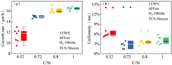
Figure 1.
Growth rate (a) and thickness uniformity (b) of 4H SiC epitaxial layers grown on different C/Si ratios. The red square, blue circle, yellow triangle, and green inverted triangle represent multiple sample data when the C/Si ratio is 0.52, 0.72, 0.8, and 1, respectively. Next to them is a statistical box plot. The white horizontal lines and squares in the box indicate the median and average of data statistics, respectively. Additionally, the horizontal line connecting the upper and lower parts of the box indicates the normal range. When there are scattered points separating from the box above and below, it is an abnormal value separating from the general data.
In Figure 1b, the impact of different C/Si ratios on the thickness uniformity of the 4H-SiC epitaxial layer is presented. As the growth rate changes, the thickness uniformity of the layer decreases from 7% at a C/Si ratio of 0.52 to 4% at a C/Si ratio of 0.72. Furthermore, the thickness uniformity remains stable at around 4% as the C/Si ratio increases. According to Figure 1a,b, the growth rate of the 4H-SiC epitaxial layer is both fast and stable, and the surface morphology is optimal when the C/Si ratio is 1. Previous studies have shown that the utilization efficiency of the precursor was improved, and the formation of by-products was reduced when using this C/Si ratio [23]. Therefore, it is recommended to increase the C/Si ratio of the source gas within a certain range to enhance the surface morphology of the epitaxial layer.
The study observed two thickness distributions of 4H-SiC epilayers with varying C/Si ratios, as illustrated in Figure 2. As the C/Si ratio increased, the epitaxial layer transitioned from an N-shaped distribution to a U-shaped distribution. When comparing Figure 2a to Figure 1b, it was found that the thickness uniformity of the epitaxial layer was at its lowest when the C/Si ratio was 0.52. Upon comparing Figure 1 and Figure 2, it is evident that the growth rate, thickness uniformity, and thickness distribution exhibit significant improvement and stability when the C/Si ratio is maintained at 0.72.
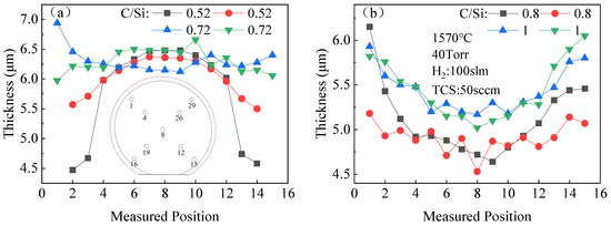
Figure 2.
The thickness distribution of 4H-SiC epitaxial layers grown at different C/Si ratios, C/Si ratio 0.52~0.72 (a), 0.8~1 (b). In the inset of (a), the solid circle indicates the wafer edge, the dashed circle is 5 mm away from the wafer edge, inside which the numbers indicate the measured positions.
During the growth of 4H-SiC, N and C atoms compete on the surface, with N replacing the lattice site of C. This leads to a notable increase in the doping efficiency of N2 in a Si-rich environment. However, the doping efficiency decreases in a C-rich environment due to the site competition effect [18]. This study compared the effects of different N2 flow rates on the carrier concentration of the 4H-SiC epitaxial layer under two C/Si ratios, as illustrated in Figure 3. The results showed that as the C/Si ratio increased from 0.8 to 1, the doping concentration decreased significantly. Furthermore, the decrease in doping concentration was more pronounced with the increase in N2 flow rate. The doping uniformity can be improved by decreasing the N2 flow rate and increasing the C/Si ratio. It is recommended to adjust the N2 flow rate based on the C/Si ratio to achieve the highest doping concentration and uniformity.
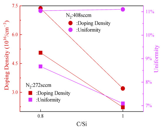
Figure 3.
Doping density and doping uniformity of 4H-SiC epitaxial layers grown at different C/Si ratios and N2 flow rates.
The quality of 4H-SiC epitaxial layers varies greatly with different C/Si ratios, as shown in Figure 4. The surface morphology of the 4H-SiC epitaxial layer with a C/Si ratio of 0.8 is the worst, as indicated by both the average value and the fluctuation of the data. Although the average values of surface roughness of 4H-SiC epitaxial layers with C/Si ratios of 0.52, 0.72, and 1 are not significantly different, the roughness data of 4H-SiC epitaxial layers have the smallest fluctuation when the C/Si ratio is 0.72. It is speculated that if the C/Si ratio is either too high or too low, it may result in the formation of two-dimensional island nucleation of 3C-SiC polycrystalline.
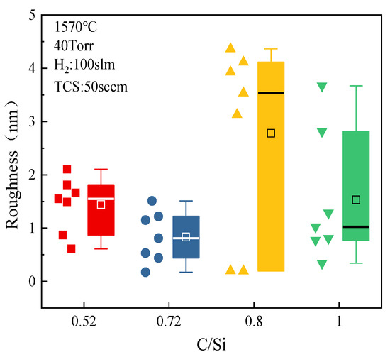
Figure 4.
The average surface roughness of 4H-SiC epitaxial layers grown at different C/Si ratios. The red square, blue circle, yellow triangle, and green inverted triangle represent multiple sample data when the C/Si ratio is 0.52, 0.72, 0.8, and 1, respectively. Next to them is a statistical box plot. The white horizontal lines and squares in the box indicate the median and average of data statis-tics, respectively. Additionally, the horizontal line connecting the upper and lower parts of the box indicates the normal range.
In order to assess the quality of 4H-SiC epitaxial layers grown at varying C/Si ratios, the surface roughness of the epitaxial layer was analyzed using AFM in a 10 μm × 10 μm region. This is illustrated in Figure 5. In conclusion, the C/Si ratio plays a significant role in determining the morphology and quality of the 4H-SiC epitaxial layer.
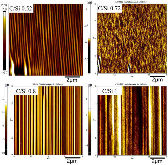
Figure 5.
AFM images of a 10 μm × 10 μm area of the 4H-SiC epitaxial layer with different C/Si ratios.
3.2. Effect of Temperature
Temperature plays a crucial role in the epitaxial growth of 4H-SiC. In our experiment, we maintained a C/Si ratio of 0.72, H2 flow rate of 100 slm, TCS flow rate of 50 sccm, N2 flow rate of 76 sccm, and growth time of 25 min. At the same time, the temperature varied from 1510 °C to 1570 °C to study the effect of temperature on the 4H-SiC epitaxial layer. Results showed that, as temperature increased, the surface roughness of the epitaxial layer decreased rapidly from 32.02 nm (1510 °C) to 3.47 nm (1530 °C) and then slowly decreased to 0.81 nm (1570 °C). The findings suggest that the increase in temperature enhances the migration of atoms on the substrate surface, leading to a reduction in the roughness of the epitaxial layer, as depicted in Figure 6b.
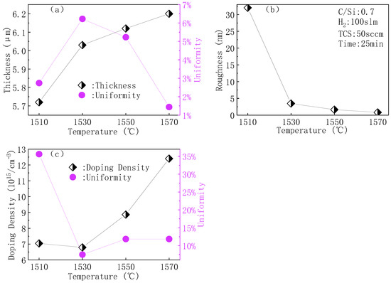
Figure 6.
The thickness and thickness uniformity (a), surface roughness (b), doping concentration, and doping uniformity (c) of the 4H-SiC epitaxial layer at different temperatures.
Figure 6a demonstrates a gradual increase in the thickness of the epitaxial layer with an increase in temperature. At the highest temperature (1570 °C), the thickness reaches 6.2 μm. This indicates that the deposition rate surpasses the etching rate of H2. Similarly, as the temperature increased to 1570 °C, the uniformity of thickness increased to 1.44%. This is due to the acceleration of intermediate product formation, which not only improves the uniformity of the epitaxial layer thickness but also increases the deposition rate.
As shown in Figure 6c, it can be observed that the N2 doping efficiency of the epitaxial layer increases with an increase in temperature. This observation is consistent with previous reports, suggesting that the thermal activation process plays a crucial role in incorporating N2 [26]. The uniformity of N2 doping is observed to be good (7.5%) at a temperature of 1530 °C. However, it deteriorates (11.5%) with a further increase in temperature. The increase in temperature leads to an increase in the total doping efficiency of N2. However, the uneven temperature distribution during heating causes variations in doping efficiency across different regions of the 4H-SiC substrate. Consequently, this uneven distribution of temperature affects the uniformity of N2 doping.
3.3. Effect of TCS Flow Ratio
SiC devices have varying specifications, including differences in the thickness and doping concentration of the epitaxial layer. The use of TCS as a Si source has demonstrated a significant improvement in growth rate compared to the traditional SiH4 + C3H8 + H2 growth system. However, researchers have continued to focus on achieving higher rates of 4H-SiC homoepitaxial growth. This section specifically examines the impact of different TCS flow rates on the growth rate of 4H-SiC epitaxial layers. In this experiment, the H2 flow rate was set to 100 slm, growth pressure to 40 torr, C/Si ratio to 1, and growth temperature to 1570 °C. Three different TCS flow rates, 30 sccm, 60 sccm, and 70 sccm, were used for a growth time of 30 min. The effects of different TCS flow rates on the thickness and uniformity of the epitaxial layer are shown in Figure 7a. The thickness of the epitaxial layer increases linearly with the increase of TCS flow rate, but its uniformity improves and then worsens with the increase of gas flow rate. It is speculated that the airflow in the reaction chamber becomes disordered after the gas flow rate increases.
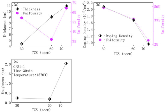
Figure 7.
The influence of TCS flow rate on the thickness and uniformity of the epitaxial layer (a) and the effect on doping concentration and its uniformity (b), the influence on the epitaxial layer roughness (c).
In Figure 7b, the effect of TCS flow on doping concentration and its uniformity is shown. As the TCS flow rate increases, the doping concentration gradually decreases, but the uniformity of the doping concentration improves. This is because no additional N2 gas is introduced during the experiment, leading to more N2 in the reaction chamber being taken away with the increase of the growth source gas. This results in a gradual decrease in the doping concentration and an increase in the uniformity of doping concentration.
The high market price of SiC epitaxial wafers can be attributed to the slow growth rate and high cost of 4H-SiC homoepitaxial growth. It is interesting to note that the bond energy between chlorine and silicon is stronger than that of silicon with other elements such as fluorine, bromine, and iodine. Specifically, the bond energies of Si-Si, Si-F, Si-Cl, Si-Br, and Si-I are 226, 597, 400, 330, and 234 kJ/mol, respectively [27]. The high reactivity of halogen-containing compounds makes it easier for them to bond with Si during epitaxial growth. At temperatures ranging from 1300 °C to 1700 °C, non-polymerizable compounds are formed and can be discharged as reaction by-products through the tail gas pipeline. Introducing halogen compounds into the traditional growth system can significantly improve the growth rate and obtain a better-quality epitaxial layer. In this experiment, as shown in Figure 7c, the surface roughness of the epitaxial layer initially decreases and then increases with the increase of the TCS flow rate. This could be due to the formation of other by-products or an increase in falling objects, which requires further testing.
3.4. Effect of N2 Flow
SiC devices have varying specifications based on the carrier concentrations of the SiC epitaxial layer. Inaccurate control of the doping concentration can lead to high on-resistance or substandard reverse withstand voltage of the device [28]. Compared to Si, doping SiC devices through ion implantation is more challenging. Typically, SiC doping is achieved by incorporating a doping source during the epitaxial process. Similar to the precise injection dose and depth of ion implantation in the Si process, the doping concentration of SiC epitaxial layers must also be accurately controlled. SiC devices with electrons as majority carriers exhibit better performance than those with holes as majority carriers, as the electron mobility of SiC is significantly higher than the hole mobility [29]. This section aims to investigate the impact of N2 on the doping concentration of the epitaxial layer. Samples with varying C/Si ratios (0.52, 0.72, 0.8, and 1) were selected to determine the doping concentration and uniformity under different N2 flow rates.
The influence of different N2 flow rates on doping concentration with a C/Si ratio of 1 is shown in Figure 8a. The doping concentration does not increase linearly with the increase of the N2 flow rate. When the N2 flow rate is between 13 and 15 sccm, the doping concentration is smaller than without N2. However, the doping concentration gradually increases with the increase of the N2 flow rate and greatly improves the uniformity of doping concentration. In Figure 8b, the effect of the N2 flow rate on doping concentration is demonstrated when C/Si is 0.8. As the N2 flow rate increases, the doping concentration gradually increases and reaches its peak at a rate of 428 sccm. After this point, there is a slight decrease in doping concentration with a further increase in the N2 flow rate until it begins to increase again after the rate surpasses 800 sccm. The doping concentration uniformity is at its worst when the N2 flow rate is 600 sccm but improves significantly as the rate continues to increase. Figure 8c depicts the impact of the N2 flow rate on doping concentration for a C/Si ratio of 0.72. As the N2 flow rate increases, the doping concentration also increases in a nearly linear fashion. However, the uniformity of doping concentration gradually worsens. Figure 8d illustrates the impact of the N2 flow rate on doping concentration for a C/Si ratio of 0.52. As the N2 flow rate increases, there is a linear increase in doping concentration in the epitaxial layer, and the uniformity of doping concentration improves gradually. Therefore, the effect of the N2 flow rate on doping concentration is dependent on the C/Si ratio during growth.
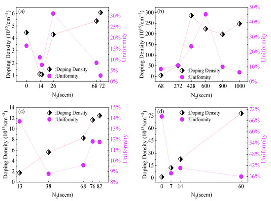
Figure 8.
The effect of N2 flow rate on doping concentration, C/Si = 1 (a), C/Si = 0.8 (b), C/Si = 0.72 (c), C/Si = 0.52 (d).
3.5. Effect of N2 Flow Ratio
To examine the impact of the N2 flow ratio on doping, an experiment was conducted at a growth temperature of 1570 °C and a constant C/Si ratio of 1. The reaction chamber was equipped with both the main gas flow channel and side gas flow channel to address differences in doping concentration between the central and edge regions of the epitaxial layer due to temperature distribution and uneven airflow. To observe the doping concentration distribution in the radial direction of the epitaxial layer, the N2 flow ratio was varied from 1 to 1.78. Figure 9a shows that the doping concentration curve is convex at an N2 flow ratio of 1.25. However, for the other three N2 flow ratios, the middle of the doping curve is slightly convex, resulting in a W-shaped curve overall. In addition, the epitaxial layer’s doping concentration increases as the N2 flow ratio increases. Figure 9b shows the doping uniformity of the layer at various N2 flow ratios. The highest doping uniformity of 11.67% was achieved at an N2 flow ratio of 1.78. The results indicate that adjusting the N2 flow ratio can alter the doping concentration distribution and uniformity in the relevant area. Furthermore, a higher N2 flow ratio leads to better doping concentration and uniformity. Future research can further investigate the impact of a higher N2 flow ratio on doping.
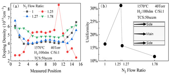
Figure 9.
The effect of N2 flow ratio on radial doping concentration distribution (a) and doping uniformity (b).
4. Conclusions
In this study, a 150 mm 4° off-axis substrate was used to grow a homoepitaxial layer of 4H-SiC using a horizontal hot-wall CVD reactor. The research focused on analyzing the impact of the C/Si ratio, growth temperature, and N2 flow ratio on the growth rate, doping, surface roughness, and uniformity of the large-size 4H-SiC epitaxial layer. The parameters were varied to determine their effect on the aforementioned characteristics. As the C/Si ratio increases, so does the average growth rate of the epitaxial layer. A stable and uniform thickness of the epitaxial layer (4%) can be achieved when the C/Si ratio is not less than 0.72. It is important to adjust the N2 flow rate in a timely manner based on the C/Si ratio to achieve the optimal epitaxial layer doping concentration and uniformity. At the same time, the change in the C/Si ratio will affect the surface roughness of the epitaxial layer.
TCS flows (30 sccm, 60 sccm, and 70 sccm) were utilized with a growth time of 30 min. As the TCS flow rate increased, the thickness of the epitaxial layer also increased linearly. However, the uniformity of the epitaxial layer improved initially and then worsened with the increase in gas flow rate. It is hypothesized that an increase in gas flow rate results in disordered airflow within the reaction chamber, subsequently causing a decline in the uniformity of the epitaxial layer. Additionally, the doping concentration decreased gradually with the increase of TCS flow rate, while the uniformity of doping concentration improved. The absence of N2 gas may have contributed to this phenomenon. Furthermore, the surface roughness of the epitaxial layer decreased initially and then increased with the increase of the TCS flow rate. This may be due to the formation of other by-products or the increase of falling objects. The effect of the N2 flow rate on doping concentration in the sample epitaxial layer is not always linear and is dependent on the C/Si ratio during growth. When the C/Si ratio is 1 and 0.8, the doping concentration does not increase linearly with the increase of the N2 flow rate, but the uniformity of doping concentration is good. However, when the C/Si ratio is 0.72 and 0.62, the doping concentration increases linearly with the increase of the N2 flow rate. This may be because the lower C/Si ratio leads to fewer C atoms, allowing N atoms to combine with more vacancies. The doping concentration uniformity is generally good, except when the C/Si ratio is 0.72, where it is poor. Therefore, it can be concluded that the effect of the N2 flow rate on doping concentration is related to the C/Si ratio during growth.
As temperature increases, the migration of atoms on the substrate surface becomes more pronounced, resulting in a maximum epitaxial layer thickness of 6.2 μm and thickness uniformity of 1.44% at 1570 °C. Additionally, the roughness of the epitaxial layer is reduced, reaching a minimum value of 0.81 nm. As temperature increases, doping concentration also increases; however, this leads to a decrease in the uniformity of doping due to uneven temperature distribution. To address this issue, adjusting the N2 flow ratio can compensate for the difference in thickness and doping concentration between the central and edge regions of the epitaxial layer caused by temperature distribution and uneven airflow. In particular, the best doping uniformity of 11.67% was achieved at a growth temperature of 1570 °C and a N2 flow ratio of 1.78. Thus, the C/Si ratio, growth temperature, and N2 flow ratio are crucial parameters for the growth of high-quality 4H-SiC homoepitaxial layers on 150 mm 4° off-axis substrates.
Author Contributions
Data curation, methodology, formal analysis, writing—original draft preparation, W.Y.; software, visualization, validation, Y.P.; investigation, formal analysis, N.G.; supervision, resources, investigation, Y.L.; project administration, investigation, supervision, X.Z.; conceptualization, supervision, funding acquisition, writing—review and editing, X.L. All authors have read and agreed to the published version of the manuscript.
Funding
This work was supported by the National Key R&D Program of China (Grant No. 2021YFB3401603) and the National Natural Science Foundation of China (Grant No. 12175236).
Data Availability Statement
The data that support the findings of this study are available from the corresponding authors, X.Z. and X.L., upon reasonable request.
Conflicts of Interest
The authors declare no conflict of interest.
References
- Chen, W.; Capano, M.A. Growth and Characterization of 4H-SiC Epilayers on Substrates with Different Off-Cut Angles. J. Appl. Phys. 2005, 98, 114907. [Google Scholar] [CrossRef]
- Chen, J.; Guan, M.; Yang, S.; Zhao, S.; Yan, G.; Shen, Z.; Zhao, W.; Wang, L.; Liu, X.; Sun, G.; et al. Characterization of Epitaxial Layers Grown on 4H-SiC (000-1) Substrates. J. Cryst. Growth 2023, 604, 127048. [Google Scholar] [CrossRef]
- Strupinski, W.; Grodecki, K.; Wysmolek, A.; Stepniewski, R.; Szkopek, T.; Gaskell, P.E.; Grueneis, A.; Haberer, D.; Bozek, R.; Krupka, J.; et al. Graphene Epitaxy by Chemical Vapor Deposition on SiC. Nano Lett. 2011, 11, 1786–1791. [Google Scholar] [CrossRef]
- Matsunami, H.; Kimoto, T. Step-Controlled Epitaxial Growth of SiC: High Quality Homoepitaxy. Mater. Sci. Eng. R Rep. 1997, 20, 125–166. [Google Scholar] [CrossRef]
- Zhao, S.; Chen, J.; Yang, S.; Yan, G.; Shen, Z.; Zhao, W.; Wang, L.; Liu, X.; Sun, G.; Zeng, Y. Effect of Temperature on Growth of Epitaxial Layer on Semi-Insulating 4H-SiC Substrate. J. Cryst. Growth 2023, 603, 127008. [Google Scholar] [CrossRef]
- Shenai, K.; Dudley, M.; Davis, R.F. Current Status and Emerging Trends in Wide Bandgap (WBG) Semiconductor Power Switching Devices. ECS J. Solid State Sci. Technol. 2013, 2, N3055–N3063. [Google Scholar] [CrossRef]
- Roccaforte, F.; Fiorenza, P.; Greco, G.; Lo Nigro, R.; Giannazzo, F.; Iucolano, F.; Saggio, M. Emerging Trends in Wide Band Gap Semiconductors (SiC and GaN) Technology for Power Devices. Microelectron. Eng. 2018, 187, 66–77. [Google Scholar] [CrossRef]
- Saitoh, Y.; Itoh, H.; Wada, K.; Sakai, M.; Horii, T.; Hiratsuka, K.; Tanaka, S.; Mikamura, Y. 150 A SiC V-Groove Trench Gate MOSFET with 6 × 6 Mm (2) Chip Size on a 150 Mm C-Face In-House Epitaxial Wafer. Jpn. J. Appl. Phys. 2016, 55, 04ER05. [Google Scholar] [CrossRef]
- Pons, M.; Blanquet, E.; Dedulle, J.M.; Ucar, M.; Wellmann, P.; Danielsson, O.; Ferret, P.; Di Cioccio, L.; Baillet, F.; Chaussende, D.; et al. Progress and Limits of the Numerical Simulation of SiC Bulk and Epitaxy Growth Processes. In Silicon Carbide and Related Materials 2004; Nipoti, R., Poggi, A., Scorzoni, A., Eds.; Trans Tech Publications Ltd.: Durnten-Zurich, Switzerland, 2005; Volume 483, pp. 3–8. ISBN 978-0-87849-963-2. [Google Scholar]
- Wellmann, P.J. Review of SiC Crystal Growth Technology. Semicond. Sci. Technol. 2018, 33, 103001. [Google Scholar] [CrossRef]
- Cooper, J.A.; Agarwal, A. SiC power-switching devices-the second electronics revolution? Proc. IEEE 2002, 90, 956–968. [Google Scholar] [CrossRef]
- Tu, R.; Liu, C.; Xu, Q.; Liu, K.; Li, Q.; Zhang, X.; Kosinova, M.L.; Goto, T.; Zhang, S. Epitaxial Growth of SiC Films on 4H-SiC Substrate by High-Frequency Induction-Heated Halide Chemical Vapor Deposition. Coatings 2022, 12, 329. [Google Scholar] [CrossRef]
- Hassan, J.; Bergman, J.P.; Henry, A.; Janzén, E. In-situ surface preparation of nominally on-axis 4H-SiC substrates. J. Cryst. Growth 2008, 310, 4430–4437. [Google Scholar] [CrossRef]
- Hassan, J.; Bergman, P.; Palisaitis, J.; Henry, A.; McNally, P.J.; Anderson, S.; Janzén, E. Growth and Properties of SiC On-Axis Homoepitaxial Layers Mater. In Materials Science Forum; Trans Tech Publications Ltd.: Wollerau, Switzerland, 2010; Volume 645, pp. 83–88. [Google Scholar] [CrossRef]
- Valente, G.; Cavallotti, C.; Masi, M.; Carra, S. Reduced Order Model for the CVD of Epitaxial Silicon from Silane and Chlorosilanes. J. Cryst. Growth 2001, 230, 247–257. [Google Scholar] [CrossRef]
- La Via, F.; Galvagno, G.; Foti, G.; Mauceri, M.; Leone, S.; Pistone, G.; Abbondanza, G.; Veneroni, A.; Masi, M.; Valente, G.L.; et al. 4H SiC Epitaxial Growth with Chlorine Addition. Chem. Vap. Depos. 2006, 12, 509–515. [Google Scholar] [CrossRef]
- Song, B.; Gao, B.; Han, P.; Yu, Y.; Tang, X. Numerical Simulation of Gas Phase Reaction for Epitaxial Chemical Vapor Deposition of Silicon Carbide by Methyltrichlorosilane in Horizontal Hot-Wall Reactor. Materials 2021, 14, 7532. [Google Scholar] [CrossRef]
- Zhao, L.X.; Yang, L.; Wu, H.W. High Quality 4H-SiC Homo-Epitaxial Wafer Using the Optimal C/Si Ratio. J. Cryst. Growth 2020, 530, 125302. [Google Scholar] [CrossRef]
- Liu, X.F.; Yan, G.G.; Liu, B.; Shen, Z.W.; Wen, Z.X.; Chen, J.; Zhao, W.S.; Wang, L.; Zhang, F.; Sun, G.S.; et al. Process Optimization for Homoepitaxial Growth of Thick 4H-SiC Films via Hydrogen Chloride Chemical Vapor Deposition. J. Cryst. Growth 2018, 504, 7–12. [Google Scholar] [CrossRef]
- Yang, S.; Zhao, S.; Chen, J.; Yan, G.; Shen, Z.; Zhao, W.; Wang, L.; Zhang, Y.; Liu, X.; Sun, G.; et al. Growth of 4H-SiC Epitaxial Layers at Temperatures below 1500 °C Using Trichlorosilane (TCS). J. Cryst. Growth 2023, 612, 127058. [Google Scholar] [CrossRef]
- Niu, Y.; Tang, X.; Sang, L.; Li, Y.; Kong, L.; Tian, L.; Tian, H.; Wu, P.; Jia, R.; Yang, F.; et al. The influence of temperature on the silicon droplet evolution in the homoepitaxial growth of 4H-SiC. J. Cryst. Growth 2018, 504, 37–40. [Google Scholar] [CrossRef]
- Li, Y.; Zhao, Z.; Zhu, Z.; Li, Z. Aluminum doping property in SiC epilayers grown at high growth rate using chloride-based CVD. J. Mater. Sci. Mater. Electron. 2015, 26, 2338–2342. [Google Scholar] [CrossRef]
- Yan, G.G.; He, Y.W.; Shen, Z.W.; Cui, Y.X.; Li, J.T.; Zhao, W.S.; Wang, L.; Liu, X.F.; Zhang, F.; Sun, G.S.; et al. Effect of C/Si ratio on growth of 4H-SiC epitaxial layers on on-axis and 4° off-axis substrates. J. Cryst. Growth 2020, 531, 125362. [Google Scholar] [CrossRef]
- Zhao, L.; Wu, H. A Correlation Study of Substrate and Epitaxial Wafer with 4H-N Type Silicon Carbide. J. Cryst. Growth 2019, 507, 109–112. [Google Scholar] [CrossRef]
- Yamashita, T.; Matsuhata, H.; Sekiguchi, T.; Momose, K.; Osawa, H.; Kitabatake, M. Characterization of Comet-Shaped Defects on C-Face 4H-SiC Epitaxial Wafers by Electron Microscopy. J. Cryst. Growth 2015, 416, 142–147. [Google Scholar] [CrossRef]
- Zhang, J.; Ellison, A.; Henry, A. Nitrogen Incorporation during 4H-SiC Epitaxy in a Chimney CVD Reactor. J. Cryst. Growth 2001, 226, 267–276. [Google Scholar] [CrossRef]
- Ohtani, N.; Katsuno, M.; Tsuge, H.; Fujimoto, T.; Nakabayashi, M.; Yashiro, H.; Sawamura, M.; Aigo, T.; Hoshino, T. Propagation behavior of threading dislocations during physical vapor transport growth of silicon carbide (SiC) single crystals. J. Cryst. Growth 2006, 286, 55–60. [Google Scholar] [CrossRef]
- Tsuchida, H.; Ito, M.; Kamata, I.; Nagano, M. Formation of extended defects in 4H-SiC epitaxial growth and development of a fast growth technique. Phys. Status Solidi B 2009, 246, 1553–1568. [Google Scholar] [CrossRef]
- Dudley, M.; Wu, F.; Wang, H.; Byrappa, S.; Raghothamachar, B.; Choi, G.; Sun, S.; Sanchez, E.K.; Hansen, D.; Drachev, R.; et al. Stacking faults created by the combined deflection of threading dislocations of Burgers vector c and c + a during the physical vapor transport growth of 4H–SiC. Appl. Phys. Lett. 2011, 98, 232110. [Google Scholar] [CrossRef]


Disclaimer/Publisher’s Note: The statements, opinions and data contained in all publications are solely those of the individual author(s) and contributor(s) and not of MDPI and/or the editor(s). MDPI and/or the editor(s) disclaim responsibility for any injury to people or property resulting from any ideas, methods, instructions or products referred to in the content. |
© 2023 by the authors. Licensee MDPI, Basel, Switzerland. This article is an open access article distributed under the terms and conditions of the Creative Commons Attribution (CC BY) license (https://creativecommons.org/licenses/by/4.0/).