Article

Gallium-Modified Zinc Oxide Thin Films Prepared by Chemical Solution Deposition

Jožef Stefan Institute, 1000 Ljubljana, Slovenia
*
Author to whom correspondence should be addressed.
Crystals 2023, 13(7), 1030; https://doi.org/10.3390/cryst13071030
Submission received: 30 May 2023 / Revised: 21 June 2023 / Accepted: 27 June 2023 / Published: 28 June 2023
(This article belongs to the Special Issue Advanced Electronic Ceramics)

Abstract

:
Gallium-doped ZnO (GZO) thin films on glass, which can be used as transparent electrodes, were prepared using a spin coating technique. Thermal analysis and Fourier-transform infrared spectroscopy of the dried precursor solution of Zn acetate and Ga nitrate dissolved in ethanol with diethanolamine confirmed the decomposition of the organic components upon heating and the formation of ZnO at 450 °C. The thin films fired at 600 °C in oxygen and air, and the films annealed at 400 °C in Ar/H2, were polycrystalline, 140 nm thick, and exhibited a homogeneous microstructure with 50 nm grains and a smooth surface, as shown by X-ray powder diffraction and scanning electron and atomic force microscopy. The sheet resistance Rs measured using the 4-probe technique showed a change in Rs within 80 days for all samples. The Rs of the GZO thin films annealed in oxygen and air with values of MΩ/sq decreased over time. Rs values of 150 kΩ/sq were obtained for GZO thin films annealed in Ar/H2, but the Rs increased over time. We suggest that the degradation of Rs is related to the adsorption of water on GZO and that the responses depend on the nature of the defects in the GZO lattice.

1. Introduction

Zinc oxide is a semiconductor with a wide direct band gap of 3.37 eV. In the form of a thin film, it meets the optical property requirements for optoelectronic devices, i.e., visible light transparency >80%, but not the electrical ones, i.e., specific electrical resistivity ~10−3 Ωcm and carrier concentration (n) ~1020 cm−3. ZnO exhibits n-type conductivity, which has been attributed to intrinsic defects, such as oxygen vacancies (VO) and interstitial zinc (Zni), as well as extrinsic defects intentionally or unintentionally introduced into the ZnO structure [1]. Hydrogen is frequently involved in the processing of ZnO-based thin films and has therefore been intensively investigated as a possible source of the extrinsic defect [2,3,4,5]. Hydrogen has been shown to be incorporated in the wurtzite ZnO structure in interstitial positions, always in the H+ charge state. It acts as a shallow donor and increases the concentration of free charge carriers and, thus, the electrical conductivity of ZnO [2,5].
To increase the conductivity of ZnO, it is modified with group-III dopants, such as In3+, Al3+, and Ga3+. The ionic radius of Zn2+ is 0.060 nm, while the ionic radii of Ga3+, Al3+, and In3+ are 0.047 nm, 0.039, and 0.079 nm, respectively [6]. Ga3+, whose ionic radius is most similar to that of Zn2+, decreases crystallinity and leads to lattice deformations and larger lattice parameters for Ga-doped ZnO thin films (GZO) [1,7,8,9]. Ga3+ significantly affects the intrinsic defects of ZnO. Ga3+ can occupy substitutional and interstitial sites of the ZnO crystal lattice and induce zinc vacancies, leading to the higher electrical conductivity of the ZnO [10]. However, the electrical conductivity decreases above a certain amount of Ga3+, which is attributed to a solubility limit of Ga3+ in the ZnO lattice [11,12]. When the solid solubility limit of Ga in ZnO is exceeded, it may segregate at grain boundaries, may form spinel phases such as GaZn2O4, and reduce the mobility of charge carriers [9,11,13,14]. The literature is not consistent regarding the solubility limit of Ga3+ in ZnO. For ZnO powders, it is reported to be as low as 1 atomic% [15,16], while for GZO thin films prepared by spin coating, a higher solid solubility limit of up to 5 atomic% has been reported [17].
A number of methods have been used to produce GZO thin films, e.g., magnetron sputtering [18], chemical vapor deposition (CVD) [13,19], spray pyrolysis [20], and chemical solution deposition (CSD) [11,14,21,22]. CSD offers several advantages for product commercialization, such as deposition in a vacuum-free environment, simple equipment, low fabrication costs, and effective control of the chemical stoichiometry.
The solutions for processing GZO have been prepared by dissolving precursors, such as zinc acetate and gallium nitrate, in 2-methoxyethanol with the addition of sol stabilizers (diethanolammine, monoethanolamine) [14,21,23]. Ethanol and 2-propanol-based solvents were also proposed for processing GZO thin films as an alternative to the toxic 2-methoxyethanol (2MOE) [11,17]. Regardless of the solvent, GZO thin films on glass exhibit excellent visible-light transparency of over 80%, but their resistivity values vary by several orders of magnitude. The resistivities of spin-coated GZO thin films from different solutions and under different annealing conditions are listed in Table 1.
The literature is consistent in that annealing ZnO-based thin films in a reducing atmosphere results in electrical resistivity in the range of a few mΩcm. For example, Nayak et al. [14] processed ZnO thin films with up to 5% Ga from a 2MOE-based solution on glass by spin coating. Among the air-annealed samples, the lowest sheet resistance was measured for the ZnO thin film doped with 2% Ga. Its resistivity further decreased upon post-annealing in a H2/N2 atmosphere. A similar trend was reported by Winner et al. [11], who processed GZO thin films with 1% Ga from a 2-propanol-based solution. Sbeta et al. [17] reported significantly higher values for GZO thin films obtained from ethanol-based solutions and annealing in air. However, Serrao et al. [23] processed ZnO thin films with 3% Ga, and after annealing in air, the resistivity of the film was 2.23 mΩcm, which is typical for samples annealed in this way. Jun et al. [21] processed GZO with 1.5% Ga on glass, and after annealing in air, they reported a low sheet resistance of 49.5 mΩcm. These reports are, to some extent, contradictory, and a direct comparison of the properties, especially the electrical resistivity of the GZO thin films, is extremely difficult. In particular, these reports do not provide information about whether the resistivity was measured in as-prepared or few-days- or few-weeks-aged samples. This is important because the electrical resistivity of ZnO-based thin films varies over time due to the interaction of ambient water with zinc vacancies in the ZnO lattice and/or due to the chemisorption of oxygen at the grain boundaries. Both phenomena decrease the carrier concentration and consequently increase the resistivity of the thin films [20,24,25,26,27,28].
The electrical resistivity of GZO thin films depends on many parameters. In addition to the intrinsic parameters (amount of dopant, carrier concentration), the extrinsic parameters such as thickness, crystal structure, grain size, porosity, and surface roughness affect the properties. An interpretation requires a detailed description of the solutions, processing conditions (temperature, time, atmosphere for drying and annealing), structure, microstructure, and surface analyses. In this work, we report on the thermal decomposition of the solution, structure, microstructure, surface roughness, and sheet resistance of the thin films with the composition corresponding to ZnO with 1.5% Ga and relate them to the processing conditions. We also address property variations over time. This systematic study contributes to our understanding of the processing-properties relationships for solution-derived GZO thin films.

2. Experimental

2.1. Solution

The solutions were prepared from zinc acetate dihydrate (ZAH, >99%, Zn(CH3COO)2 xH2O, Sigma–Aldrich, St. Louis, MO, USA), gallium nitrate hydrate (GNH, Ga(NO3)3 xH2O, 99.9%, Alfa Aesar, Karlsruhe, Germany), anhydrous ethanol (C2H5OH, 99.9%, Carlo Erba, Val-de-Reuil, France), and diethyleneamine (DEA, HN(CH2CH2OH)2, 99.9%, Alfa Aesar, Karlsruhe, Germany).
The solution for spin coating was prepared by mixing a Zn solution and a Ga solution. The molar ratio Ga/(Ga + Zn) was 0.015. The zinc solution with a concentration of Zn 0.66 molL−1 was prepared by dissolving ZAH in anhydrous ethanol and stirring it in a flask with a magnetic stirrer at room temperature for 1 h. A suitable amount of DEA is dissolved in a small volume of anhydrous ethanol and then gradually added to the zinc solution until a clear solution is obtained. The molar ratio of DEA to ZnAH was maintained at 1:1. The gallium solution with a concentration of 0.009 molL−1 was prepared by dissolving GNH in anhydrous ethanol.
The GZO solution with a concentration of 0.3 molL−1 (S-GZO) was prepared by mixing zinc and gallium solutions in a volume ratio of 1:1. All the solutions were transparent, free of particles, and stable for more than one month in a refrigerator. The surface tension of the precursor solution and its contact angle on the glass substrate was measured with a tensiometer (DSA20E, Krüss, Hamburg, Germany) at room temperature.
Thermal decomposition of the solution was studied by thermogravimetry (TG), differential thermal analysis (DTA), and evolved-gas analysis (EGA) using a simultaneous thermal analyzer coupled with a mass spectrometer to follow the in situ evolution of gaseous species (STA 409, Netzsch, Selb, Germany, and ThermoStar, Balzers Instruments, Oerlikon, Switzerland). Before the thermal analysis, the GZO solution was dried in air at 100 °C for 7.5 h. About 25 mg of the obtained sample was placed in a Pt crucible and heated from room temperature to 800 °C in flowing synthetic air (100 mLmin−1) at a rate of 10 K min−1.
The GZO solution was dried at 100, 300, 350, and 450 °C for 2 h. The resulting powders were analyzed with Fourier-transform infrared spectroscopy (FTIR) using a Perkin Elmer Spectrum 100. The transmittance data were collected in the range 380–4000 cm−1 in the attenuated total reflectance (ATR) mode.

2.2. Thin Films by Spin Coating

The GZO precursor solution was deposited on soda-lime glass (square shape with dimensions 12 mm × 12 mm, Corning Eagle XG) by spin coating at 3000 min−1 for 30 s (Headway research). Each layer was heated on a hot plate at 200 °C for 2 min and subsequently at 350 °C for 2 min. The procedure was repeated four times, after which the samples were annealed at 600 °C for 15 min in oxygen (GZO_O) and air (GZO_A). The GZO_A was subsequently heated to 400 °C for 60 min in Ar/H2 (GZO_H). GZO thin films were stored at room temperature and 20% relative humidity.

2.3. Structural and Microstructural Characterization of Thin Films

The thin films were examined with grazing incidence (GI) X-ray diffraction (XRD) using a Malvern PANalytical Empyrean diffractometer (Almelo, The Netherlands) with Cu-Kα1 radiation (λ = 1.5406 Å) at 45 kV and 40 mA. A hybrid monochromator with a 1/16° slit was used on the incident-beam side, and a parallel plate collimator was used on the diffracted-beam side. The GI angle (ω) was fixed at 1°. The diffractograms were collected in the 2θ range from 20° to 60° with a step size of 0.02° and a counting time of 20 s.
The surface and fracture cross-section of the thin films were investigated with a field-emission scanning electron microscope (Verios 4G HP, FE-SEM, Thermo Fischer, Waltham, Massachusetts, USA). Before the analysis, the films were coated with a 1 nm thick Au/Pd layer using a PECS 682 (Gatan, Pleasanton, CA, USA).
The surfaces of the films were examined with an atomic force microscope (AFM, Jupiter XR, Asylum Research, Oxford Instruments, Santa Barbara, CA, USA). Silicon AFM tips (OMCL-AC240TS-R3, Olympus, Japan) were used to scan in AC topography mode. Areas of 1 µm × 1 µm and 20 µm × 20 µm were scanned, and the surface root-mean-square roughness (RMS) was calculated.

2.4. Electrical Resistivity of Thin Films

The sheet resistance (Rs) of the thin films was measured using the 4-point probe technique [29], with the probes arranged equidistantly in a line. The Rs of the thin film was calculated from the measured voltage drop (V) between the two inner probes and the current (I) that is applied through the outer probe using the following equation:
R s = C π ln 2 Δ V I
where C is a correction factor. For a square-shaped sample with dimensions of 12 mm × 12 mm and a spacing s of 1.5 mm, C = 0.88. The resistivity of the film is obtained by multiplying Rs by the film thickness.

3. Results

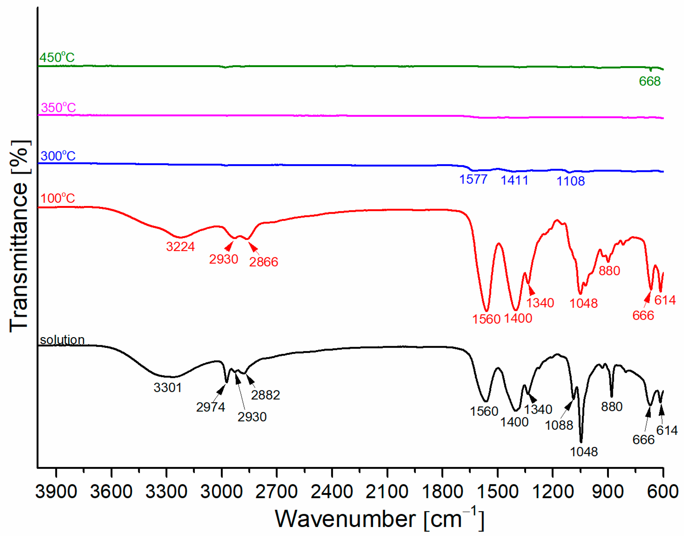
3.1. Precursor Solution

The S-GZO precursor solution was transparent, free of particles, and stable for at least two weeks in the refrigerator. Its surface tension was 20 mNm−1. The S-GZO droplet spread out completely on the glass substrate, corresponding to a contact angle of 0°.
To investigate the thermal decomposition of the precursors, we thermally analyzed the S-GZO solution, dried at 100 °C. The thermogravimetric, differential thermal analysis, and evolved-gas analysis (TG-DTA-EGA) were recorded in the air, and the curves are shown in Figure 1. The thermal decomposition occurred in four steps, with a total weight loss of 65.9%. Between 100 and 250 °C, the mass loss of 7.7% corresponds to the elimination of water, confirmed by the ion fragment m/z of 18. Between 250 and ~350 °C, the sample lost the largest mass of 32.3%. This process is accompanied by an endothermic peak at 268 °C and an exothermic peak at 295 °C. Between 350 and 410 °C, the mass loss of 13.0% is accompanied by an exothermic peak at 365 °C. Between 410 to 500 °C, the sample lost 13.0%, and this is accompanied by the most intensive, broad, and asymmetric exothermic peak at 470 °C. No further weight loss can be observed at above 500 °C, indicating the organic-free composition. The mass loss between ~250 and 410 °C is assigned to the evolution of gases with ion fragments m/z of 18, 46, and 60, while the m/z values of 18 and 46 were detected between 400 and 500 °C. These results suggest that the formation of GZO proceeds through forming a Zn-acetate-DEA complex in the ethanol solution [22,30]. Upon heating, the Zn-acetate-DEA complex re-coordinated to an intermediate compound, followed by the DEA and acetate elimination and the formation of an oxozinc complex. This process occurred between 250 and 400 °C, as is evident from the endothermic (re-coordination) and exothermic (thermal decomposition) peaks and the mass loss due to acetate and NOx elimination. With a further increase in temperature to 500 °C, the oxozinc complex changed to ZnO, accompanied by the exothermic process of CO2 and water elimination and crystallization of ZnO, in agreement with [22,31].
To complement the results of the thermal analyses, we performed FTIR analyses on S-GZO and powders obtained after drying S-GZO at 100, 300, 350, and 450 °C (Figure 2).
The FTIR spectrum of the GZO powder dried at 100 °C is similar to that of the S-GZO solution. The bands at 3200–3500 cm−1 are assigned to O-H and N-H stretching vibrations, while those at 2930 and 2866 cm−1 are assigned to C-H stretching vibrations. The bands at 1560 and 1400 cm−1 belong to the asymmetrical stretching of C=O and the symmetric stretching of COO. The difference between the asymmetric and symmetric bands of 160 cm−1 is typical for bridging complexes. The band at 1340 cm−1 can be related to C-H; 1088 cm−1 to secondary or tertiary amines; 1048 cm−1 to C-O; 880 cm−1 to N-H; and 666 cm−1 and 614 cm−1 to COO. The results confirm the formation of a Zn–acetate–DEA complex in the S-GZO solution and indicate its similar structure at 100 °C. In the FTIR spectrum of the powder heated to 300 °C, we can observe peaks with very low intensities at 1577 cm−1 and 1411 cm−1, characteristic for C=O and COO, and characteristic peaks for amines at 1108 cm−1, while the peaks that correlated with the vibrations of O-H and C-H vanished. This indicates that most of the Zn–acetate–DEA intermediate complex transformed to an oxozinc complex at 300 °C. In the powder heated to 350 °C, the organic compounds were not detected. At 450 °C, we detected only one peak at 668 cm−1, characteristic of ZnO [32,33,34].
The formation temperatures of the individual complexes and ZnO determined with the thermal analysis and FTIR are different. We believe that the difference is due to the unequal drying process. The thermal analyses were performed dynamically upon heating at a rate of 10 °C/min, while the powders were placed in a dryer for 7.5 h prior to the FTIR analyses.
Based on the thermal and FTIR analysis of the dried GZO precursor solution, we selected the annealing conditions for processing the GZO thin films: drying at 200 °C for 2 min and subsequently at 350 °C for 2 min, followed by annealing at 600 °C for 15 min in air and oxygen.

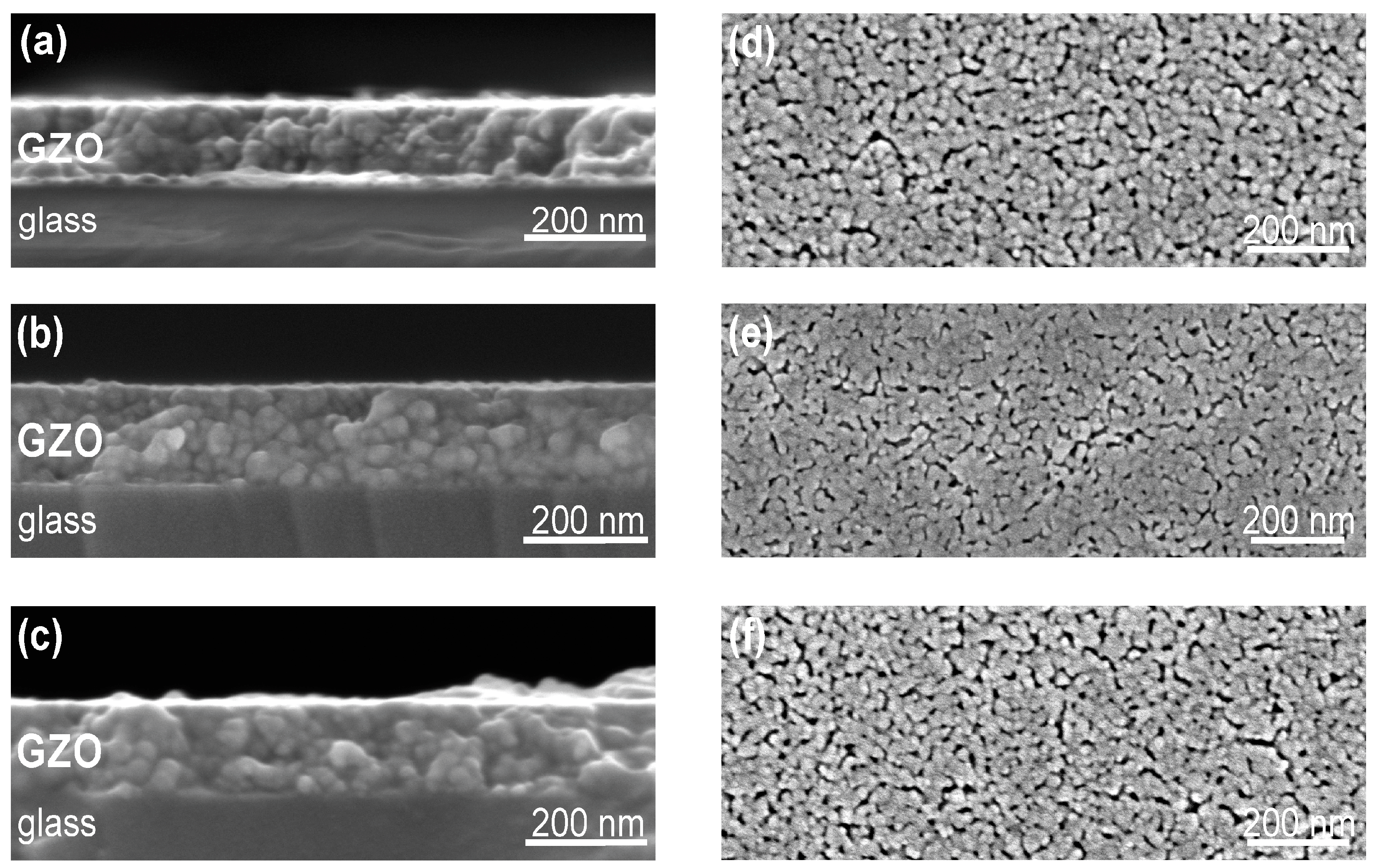
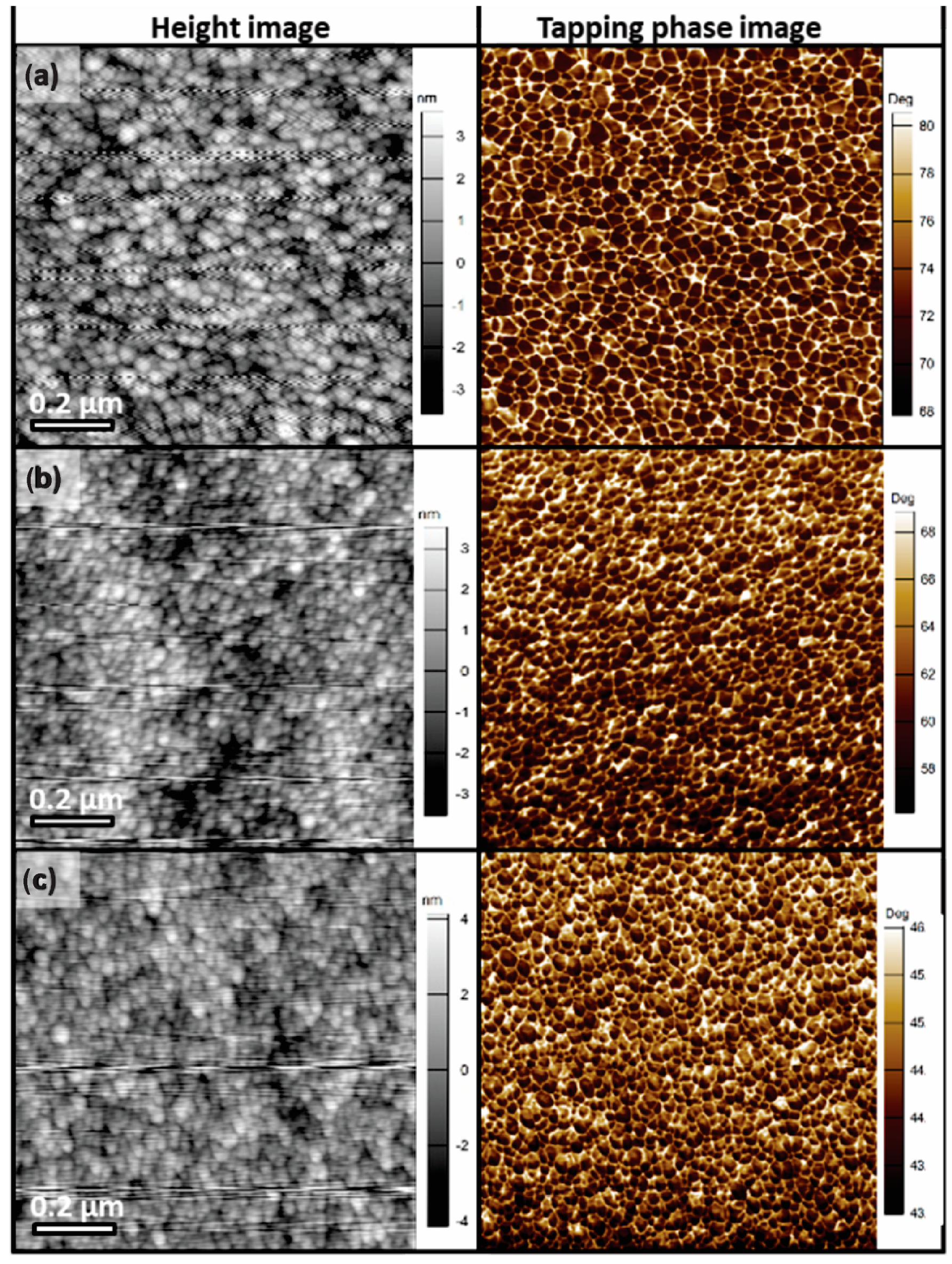
3.2. Microstructure and Electrical Properties of GZO Thin Films

The XRD patterns of the GZO-O, GZO_A, and GZO_H thin films shown in Figure 3 are similar. All the characteristic diffraction peaks belong to the hexagonal wurtzite structure of ZnO (PDF 01-75 9742). The high intensity of the (002) diffraction peak indicates a preferential crystal orientation in the c-axis, perpendicular to the glass substrate. The c-axis crystal orientation has been reported for GZO thin films on glass [9,17,20].
Figure 4 shows representative SEM images of the fracture cross-section and the surfaces of the GZO thin films annealed in oxygen, air, and Ar/H2.
The cross-section SEM images reveal that the microstructures of the GZO thin films on the glass substrate are homogeneous, with predominantly spherical, nanometer-sized grains. The X-ray photoelectron spectroscopy (XPS) analysis confirms the presence of Ga in the GZO thin films (Supplementary Information Figures S2 and S3). The thickness of the films is uniform and similar for all samples, regardless of the annealing atmosphere ~140 nm. The surface images of the films show that the nanoscale grains are separated by pores, both of which are homogeneously distributed on the surface. The surfaces of the films, analyzed by AFM (Figure 5), had grains with sizes from a few nm to ~50 nm in all samples. The surfaces were smooth with an RMS surface roughness ~2 nm, measured for a 20 μm × 20 μm region, on all three surfaces (Supplementary Materials, Figure S1). These results demonstrate that the structure, grain size, porosity, and surface roughness of the GZO thin films do not depend on the firing atmosphere, air, or oxygen and that these properties remained similar after annealing the sample in Ar/H2 at 400 °C.
After the preparation, the samples were kept in the laboratory at room temperature and a relative humidity of 20%. The sheet resistance Rs of the GZO_O, GZO_A, and GZO_H thin films was measured during the course of 80 days. The results shown in Figure 6 reveal that: (i) The annealing atmosphere of the GZO thin films has an impact on their Rs; the largest Rs was measured for the as-prepared thin films annealed in oxygen and the lowest for those annealed in a reducing atmosphere. (ii) The Rs varied in the course of 80 days; it decreased over time for GZO_O and GZO_A, while it increased slightly over time for GZO_H.
The decrease in Rs values for the GZO thin films annealed in a reducing atmosphere is related to the increase in the charge-carrier concentration and/or their mobility. The parameters affecting the carrier mobility, such as crystallinity, grain size, porosity, thickness, and surface roughness, are similar for all three samples. The carrier concentration in the GZO_O and the GZO_A originates mainly from the Ga3+ substitution at the Zn2+ sites or interstitials and/or oxygen vacancies, all acting as n-type donors [14,28,35]. The initial Rs (Rsi) of GZO_O and GZO_A was 4.26 MΩ/sq and 2.75 MΩ/sq, respectively. When the ZnO-based thin films are annealed in Ar/H2, the hydrogen atoms are incorporated in the ZnO lattice and also act as donors, which increases the carrier concentration and decreases Rs [5]. Since the nominal Ga3+ concentration was identical in all thin films, the decrease in Rs for the GZO_H could be related to the larger quantity of oxygen vacancies and incorporation of hydrogen atoms in the GZO thin films, which is reflected in the lowest Rsi of 150 kΩ/sq.
We found that Rs for the GZO thin films stored at room temperature and in 20% relative humidity varied over time. After 80 days, the Rs value for GZO_O and GZO_A decreased to 16% and 7% of the Rsi, while the Rs value for GZO_H increased to 230% Rsi.
To our knowledge, the decrease of Rs over time has never been reported for GZO thin films. However, it has been shown that the resistivity of ZnO-based thin films processed in the air decreases with increasing humidity due to water adsorption on their surfaces [36,37,38]. Thus, we placed the 80-day-old GZO_O and GZO_A thin films in a dryer at 105 °C for 30 min in the air. We found that Rs increased from 720 kΩ/sq to 950 kΩ/sq for GZO_O and from 190 kΩ/sq to 2450 kΩ/sq for GZO_A. The Rs value recovered to 0.89 Rsi after annealing GZO_A at a relatively low temperature of 105 °C in air. A lower Rs value of 0.22 Rsi was obtained for GZO_O, which was probably due to the fact that it was annealed in air and not in oxygen. After re-annealing the GZO_A at 600 °C in air for 15 min, the Rs value recovered completely. Although the Rs of the samples increased under these annealing conditions, it can not be concluded that water contributed to the Rs increase. Thus, we stored the re-annealed GZO_A in a dry box (nitrogen atmosphere, concentration of O2 and H2O below 100 ppm). We found that the Rs decreased to 770 kΩ/sq after three days. This value is slightly lower than the Rs value obtained after storing the as-prepared GZO_A at room temperature in air at 20% relative humidity, i.e., ~1000 kΩ/sq. Our experiments on the time-dependent Rs behavior and recovery ability of GZO_A and GZO_O thin films suggest that humidity up to 20% has a minor contribution to the degradation of Rs in GZO_A and GZO_O at room temperature. The interpretation of the aging effect of the studied GZO_A and GZO_O thin films requires a systematic study and is beyond the scope of this paper.
The increase in electrical resistivity over time has been demonstrated for ZnO-based thin films [5,24,25,26,39]. It was proposed that the degradation of Rs for GZO thin films prepared by sputtering in an Ar atmosphere could be due to their interaction with the atmosphere. When these GZO thin films were exposed to atmospheric humidity, water could react with the oxygen vacancies in the ZnO lattice, causing the carrier concentration to decrease [24]. It has also been reported that in an oxygen-rich atmosphere, oxygen can adsorb on the grain boundaries of GZO thin films. It forms electron traps that reduce the charge-carrier concentration. But the hydrogen atoms in the ZnO lattice limit the adsorption of oxygen, which is reflected in a lower Rs increase with time under air atmosphere [5,20]. It has also been shown that hydrogen doping can be unstable and lead to an increase in Rs with time [39].
The interaction of water with oxygen vacancies, the chemisorption of oxygen, and the diffusion of hydrogen could be the reason for the increase in the resistivity of the GZO annealed in Ar/H2. To test the reversibility of the reactions, we re-annealed the GZO_H thin film, which was stored for 21 days at room temperature in air at a relative humidity of 20%. After re-annealing GZO_H in Ar/H2 at 400 °C for 60 min, the Rs decreased from 320 kΩ/sq to 143 kΩ/sq. The Rs after re-annealing is similar to the Rsi of GZO_H, namely 150 kΩ/sq. These results show that the phenomena occurring during the aging of GZO_H are reversible. We also measured the Rs of GZO_H thin film aged for 80 days after being placed in a dryer at 105 °C for 30 min. We found that the Rs increased from 350 kΩ/sq to 900 kΩ/sq. Why the Rs exhibited these particular values remains an open question. However, we speculate that the Rs of GZO_H increased after annealing at 105 °C in air, possibly due to water desorption and partial hydrogen elimination from GZO_H. On the other hand, water could also be desorbed from the GZO_H surface during the annealing of thin films at 400 °C in Ar/H2, and hydrogen could be reincorporated into the structure, which is reflected in the lower Rs value. Important information about the interactions of GZO_H with the atmosphere at room temperature can be obtained by measuring the Rs of samples stored in a controlled atmosphere. We placed the re-annealed GZO_H in a dry box with a nitrogen atmosphere and a concentration of both O2 and H2O below 100 ppm. After three days, the Rs decreased from 143 kΩ/sq to 125 kΩ/sq. These results imply that eliminating hydrogen from the GZO_H thin films contributes to Rs degradation over time.

4. Conclusions

We succeeded in the preparation of transparent gallium-doped ZnO thin films on glass substrates from non-toxic, alcohol-based solutions by spin coating. Using thermal and FTIR analyses, we confirmed the formation of a Zn–acetate–DEA complex in solution, which transformed into an oxozinc complex up to 300 °C and into ZnO at 450 °C. X-ray powder diffraction, electron microscopy, and atomic force microscopy showed that the GZO thin films heated at 600 °C in oxygen and air (GZO_O and GZO_A, respectively) and the films subsequently annealed in Ar/H2 (GZO_H) were polycrystalline with a similar thickness of 140 nm, homogeneous microstructure, grain size up to 50 nm, and a smooth surface with an RMS surface roughness of ~2 nm. The sheet resistance Rs determined by the 4-point probe method was several MΩ/sq for GZO_O and GZO_A and decreased significantly when the samples were fired in Ar/H2 to 150 kΩ/sq, corresponding to 2.1 Ωcm.
Similar or lower resistivity values were reported for GZO thin films prepared from solutions but for thicker films and/or thin films prepared from toxic 2-methanol solutions. We show that Rs increased for GZO_H and decreased for GZO_O and GZO_A during 80 days of sample storage at room temperature and 20% relative humidity. The interpretation of Rs decrease with time for the studied GZO_O and GZO_A thin films requires a systematic investigation, while the Rs increase with time for GZO_H can be related to hydrogen elimination. The results show that the aging effect must always be considered for GZO thin films prepared by chemical solution deposition. This is of particular importance for transparent electronics with reliable properties.

Supplementary Materials

The following supporting information can be downloaded at: https://www.mdpi.com/article/10.3390/cryst13071030/s1, Figure S1: AFM topography images; (left)-height image, (right)-tapping phase image of (a) GZO_O, (b) GZO_A, (c) GZO_H. Figure S2: XPS survey spectrum of the surface of the GZO thin film, annealed in Ar/H2. Figure S3: High-energy resolution XPS spectrum Ga 2p of the surface of the GZO thin film, annealed in Ar/H2.

Author Contributions

Conceptualization, D.K.; methodology, I.S., B.K. and H.U.; validation, visualization, and investigation, all; resources, D.K.; writing—original draft preparation, D.K., I.S. and H.U.; supervision, project administration, funding acquisition, writing—review and editing, D.K. All authors have read and agreed to the published version of the manuscript.

Funding

This research was funded by the Slovenian Research Agency, grant numbers P2-0105 and L2-4469.

Data Availability Statement

Not applicable.

Acknowledgments

We thank Janez Kovač for XPS analyses, Jena Cilenšek for performing thermal analyses, Urška Trstenjak for X-ray powder diffraction, Sabi William Konsago for help with FTIR, and Enrico Maradei (Erasmus+ internship) for help in the AFM laboratory.

Conflicts of Interest

The authors declare no conflict of interest.

References

  1. McCluskey, M.D.; Jokela, S.J. Defects in ZnO. J. Appl. Phys. 2009, 106, 071101. [Google Scholar] [CrossRef] [Green Version]
  2. Van de Walle, C.G. Hydrogen as a Cause of Doping in Zinc Oxide. Phys. Rev. Lett. 2000, 85, 1012–1015. [Google Scholar] [CrossRef] [PubMed] [Green Version]
  3. Assadi, M.H.N.; Zheng, R.K.; Li, S.; Ringer, S.R. First-Principles Investigation of Electrical and Magnetic Properties of ZnO Based Diluted Magnetic Semiconductors Codoped with H. J. Appl. Phys. 2012, 111, 113901. [Google Scholar] [CrossRef]
  4. Cox, S.F.J.; Davis, E.A.; Cottrell, S.P.; King, P.J.C.; Lord, J.S.; Gil, J.M.; Alberto, H.V.; Vilão, R.C.; Piroto Duarte, J.; Ayres de Campos, N.; et al. Experimental Confirmation of the Predicted Shallow Donor Hydrogen State in Zinc Oxide. Phys. Rev. Lett. 2001, 86, 2601–2604. [Google Scholar] [CrossRef] [PubMed]
  5. Myong, S.Y.; Lim, K.S. Highly Stable and Textured Hydrogenated ZnO Thin Films. Appl. Phys. Lett. 2003, 82, 3026–3028. [Google Scholar] [CrossRef] [Green Version]
  6. Shannon, R.D.; Prewitt, C.T. Effective Ionic Radii in Oxides and Fluorides. Acta Crystallogr. B 1969, 25, 925–946. [Google Scholar] [CrossRef]
  7. Liu, Y.; Li, Y.; Zeng, H. ZnO-Based Transparent Conductive Thin Films: Doping, Performance, and Processing. J. Nanomater. 2013, 2013, 196521. [Google Scholar] [CrossRef] [Green Version]
  8. Norton, D.P.; Heo, Y.W.; Ivill, M.P.; Ip, K.; Pearton, S.J.; Chisholm, M.F.; Steiner, T. ZnO: Growth, Doping & Processing. Mater. Today 2004, 7, 34–40. [Google Scholar] [CrossRef]
  9. Sandeep, K.M.; Bhat, S.; Dharmaprakash, S.M.; Byrappa, K. Influence of Ga Doping Ratio on the Saturable Absorption Mechanism in Ga Doped ZnO Thin Solid Films Processed by Sol–Gel Spin Coating Technique. J. Phys. Appl. Phys. 2017, 50, 095105. [Google Scholar] [CrossRef]
  10. Look, D.C.; Leedy, K.D.; Vines, L.; Svensson, B.G.; Zubiaga, A.; Tuomisto, F.; Doutt, D.R.; Brillson, L.J. Self-Compensation in Semiconductors: The Zn Vacancy in Ga-Doped ZnO. Phys. Rev. B 2011, 84, 115202. [Google Scholar] [CrossRef] [Green Version]
  11. Winer, I.; Shter, G.E.; Mann-Lahav, M.; Grader, G.S. Effect of Solvents and Stabilizers on Sol–Gel Deposition of Ga-Doped Zinc Oxide TCO Films. J. Mater. Res. 2011, 26, 1309–1315. [Google Scholar] [CrossRef]
  12. Miranda, G.G.; de Sousa e Silva, R.L.; dos Santos Pessoni, H.V.; Franco, A. Raman Spectroscopy Study of Ga-Doped ZnO Ceramics: An Estimative of the Structural Disorder Degree. Phys. B Condens. Matter 2021, 606, 412726. [Google Scholar] [CrossRef]
  13. Ponja, S.D.; Sathasivam, S.; Parkin, I.P.; Carmalt, C.J. Highly Conductive and Transparent Gallium Doped Zinc Oxide Thin Films via Chemical Vapor Deposition. Sci. Rep. 2020, 10, 638. [Google Scholar] [CrossRef] [Green Version]
  14. Nayak, P.K.; Kim, J.; Chung, S.; Jeong, J.; Lee, C.; Hong, Y. Spin-Coated Ga-Doped ZnO Transparent Conducting Thin Films for Organic Light-Emitting Diodes. J. Phys. Appl. Phys. 2009, 42, 139801. [Google Scholar] [CrossRef]
  15. Yoon, M.H.; Lee, S.H.; Park, H.L.; Kim, H.K.; Jang, M.S. Solid Solubility Limits of Ga and Al in ZnO. J. Mater. Sci. Lett. 2002, 21, 1703–1704. [Google Scholar] [CrossRef]
  16. Bernardo, M.S.; Villanueva, P.G.; Jardiel, T.; Calatayud, D.G.; Peiteado, M.; Caballero, A.C. Ga-Doped ZnO Self-Assembled Nanostructures Obtained by Microwave-Assisted Hydrothermal Synthesis: Effect on Morphology and Optical Properties. J. Alloys Compd. 2017, 722, 920–927. [Google Scholar] [CrossRef]
  17. Sbeta, M.; Serin, T.; Yildiz, A. Determination of the Critical Carrier Concentration for the Metal–Insulator Transition in Ga-Doped ZnO. J. Mater. Sci. Mater. Electron. 2018, 29, 14111–14115. [Google Scholar] [CrossRef]
  18. Appani, S.K.; Singh, D.; Nandi, R.; Sutar, D.S.; Major, S.S. Influence of Oxygen Partial Pressure on the Strain Behaviour of Reactively Co-Sputtered Ga Doped ZnO Thin Films. Thin Solid Films 2023, 764, 139624. [Google Scholar] [CrossRef]
  19. Horng, R.-H.; Ou, S.-L.; Huang, C.-Y.; Ravadgar, P.; Wu, C.-I. Effects of Ga Concentration and Rapid Thermal Annealing on the Structural, Optoelectronic and Photoluminescence Properties of Ga-Doped ZnO Thin Films. Thin Solid Films 2016, 605, 30–36. [Google Scholar] [CrossRef]
  20. Rao, P.T.; Kumar, C.S.M. Resistivity Stability of Ga Doped ZnO Thin Films with Heat Treatment in Air and Oxygen Atmospheres. J. Cryst. Process Technol. 2012, 2, 72–79. [Google Scholar] [CrossRef] [Green Version]
  21. Jun, M.-C.; Park, S.-U.; Koh, J.-H. Comparative Studies of Al-Doped ZnO and Ga-Doped ZnO Transparent Conducting Oxide Thin Films. Nanoscale Res. Lett. 2012, 7, 639. [Google Scholar] [CrossRef] [PubMed] [Green Version]
  22. Hayami, R.; Endo, N.; Abe, T.; Miyase, Y.; Sagawa, T.; Yamamoto, K.; Tsukada, S.; Gunji, T. Zinc–Diethanolamine Complex: Synthesis, Characterization, and Formation Mechanism of Zinc Oxide via Thermal Decomposition. J. Sol-Gel Sci. Technol. 2018, 87, 743–748. [Google Scholar] [CrossRef]
  23. Serrao, F.J.; Dharmaprakash, S.M. Structural, Optical and Electrical Properties of Sol–Gel Prepared Ga:ZnO Thin Film. Mater. Res. Innov. 2016, 20, 470–474. [Google Scholar] [CrossRef]
  24. Nakagawara, O.; Kishimoto, Y.; Seto, H.; Koshido, Y.; Yoshino, Y.; Makino, T. Moisture-Resistant ZnO Transparent Conductive Films with Ga Heavy Doping. Appl. Phys. Lett. 2006, 89, 091904. [Google Scholar] [CrossRef]
  25. Akazawa, H. Degradation of Transparent Conductive Properties of Undoped ZnO and Ga-Doped ZnO Films Left in Atmospheric Ambient for Several Years and Trials to Recover Initial Conductance. J. Vac. Sci. Technol. Vac. Surf. Films 2014, 32, 021512. [Google Scholar] [CrossRef]
  26. Kishimoto, Y.; Nakagawara, O.; Seto, H.; Koshido, Y.; Yoshino, Y. Improvement in Moisture Durability of ZnO Transparent Conductive Films with Ga Heavy Doping Process. Vacuum 2009, 83, 544–547. [Google Scholar] [CrossRef]
  27. Sato, Y.; Makino, H.; Yamamoto, N.; Yamamoto, T. Structural, Electrical and Moisture Resistance Properties of Ga-Doped ZnO Films. Thin Solid Films 2011, 520, 1395–1399. [Google Scholar] [CrossRef]
  28. Barasheed, A.Z.; Kumar, S.R.S.; Alshareef, H.N. Temperature Dependent Thermoelectric Properties of Chemically Derived Gallium Zinc Oxide Thin Films. J. Mater. Chem. C 2013, 1, 4122. [Google Scholar] [CrossRef]
  29. Schroder, D.K. Semiconductor Material and Device Characterization, 3rd ed.; John Wiley & Sons, Inc.: Hoboken, NJ, USA, 2005; pp. i–xv. [Google Scholar]
  30. Znaidi, L.; Soler Illia, G.J.A.A.; Benyahia, S.; Sanchez, C.; Kanaev, A.V. Oriented ZnO Thin Films Synthesis by Sol–Gel Process for Laser Application. Thin Solid Films 2003, 428, 257–262. [Google Scholar] [CrossRef]
  31. Wang, Y.; Cui, W.; Yu, J.; Zhi, Y.; Li, H.; Hu, Z.-Y.; Sang, X.; Guo, E.; Tang, W.; Wu, Z. One-Step Growth of Amorphous/Crystalline Ga2O3 Phase Junctions for High-Performance Solar-Blind Photodetection. ACS Appl. Mater. Interfaces 2019, 11, 45922–45929. [Google Scholar] [CrossRef]
  32. Liu, Z.; Jin, Z.; Li, W.; Qiu, J. Preparation of ZnO Porous Thin Films by Sol–Gel Method Using PEG Template. Mater. Lett. 2005, 59, 3620–3625. [Google Scholar] [CrossRef]
  33. Ahmadi, S.H.; Ghaffarkani, M.; Ameri, M.; Safari, N.; Mohajerani, E. Solvent Selection for Fabrication of Low Temperature ZnO Electron Transport Layer in Perovskite Solar Cells. Opt. Mater. 2020, 106, 109977. [Google Scholar] [CrossRef]
  34. Socrates, G. Infrared Characteristic Group Frequencies Tables and Charts, 2nd ed.; John Wiley & Sons, Ltd.: Chichester, UK, 1994. [Google Scholar]
  35. Oba, F.; Togo, A.; Tanaka, I.; Paier, J.; Kresse, G. Defect Energetics in ZnO: A Hybrid Hartree-Fock Density Functional Study. Phys. Rev. B 2008, 77, 245202. [Google Scholar] [CrossRef] [Green Version]
  36. Ismail, A.S.; Mamat, M.H.; Md. Sin, N.D.; Malek, M.F.; Zoolfakar, A.S.; Suriani, A.B.; Mohamed, A.; Ahmad, M.K.; Rusop, M. Fabrication of Hierarchical Sn-Doped ZnO Nanorod Arrays through Sonicated Sol−gel Immersion for Room Temperature, Resistive-Type Humidity Sensor Applications. Ceram. Int. 2016, 42, 9785–9795. [Google Scholar] [CrossRef]
  37. Lai, C.; Wang, X.; Zhao, Y.; Fong, H.; Zhu, Z. Effects of Humidity on the Ultraviolet Nanosensors of Aligned Electrospun ZnO Nanofibers. RSC Adv. 2013, 3, 6640. [Google Scholar] [CrossRef]
  38. Ghosh, M.; Ningthoujam, R.S.; Vatsa, R.K.; Das, D.; Nataraju, V.; Gadkari, S.C.; Gupta, S.K.; Bahadur, D. Role of Ambient Air on Photoluminescence and Electrical Conductivity of Assembly of ZnO Nanoparticles. J. Appl. Phys. 2011, 110, 054309. [Google Scholar] [CrossRef] [Green Version]
  39. Kushwaha, A.; Aslam, M. Hydrogen-Incorporated ZnO Nanowire Films: Stable and High Electrical Conductivity. J. Phys. Appl. Phys. 2013, 46, 485104. [Google Scholar] [CrossRef]
Figure 1. TG/DTA/EGA curves of S−GZO precursor solution dried at 100 °C. Ion fragment m/z = 18 (H2O), m/z = 44 (CO2), and m/z = 60 (CH3COOH).
Crystals 13 01030 g001
Figure 2. FTIR spectra of GZO precursor solution and powders dried at 100 °C, 300 °C, 350 °C, and 450 °C.
Crystals 13 01030 g002
Figure 3. XRD diffraction patterns of GZO thin films annealed in oxygen (GZO_O), air (GZO_A), and Ar/H2 (GZO_H). The XRD pattern of the glass substrate is shown for comparison.
Crystals 13 01030 g003
Figure 4. Fracture cross-section and surface SEM images of thin films (a,d) GZO_O, (b,e) GZO_A, and (c,f) GZO_H.
Crystals 13 01030 g004
Figure 5. AFM topography images; (left)−height image, (right)−tapping phase image of (a) GZO_O, (b) GZO_A, and (c) GZO_H.
Crystals 13 01030 g005
Figure 6. Sheet resistance Rs of the GZO_O, GZO_A, and GZO_H thin films on glass.
Crystals 13 01030 g006
Table 1. Thickness and resistivity of GZO thin films spin coated under various conditions.
CompositionSolventAnnealing
Conditions
Thickness [nm]Resistivity [Ωcm]Reference
GZO 1% Ga2-propanol580 °C, 60 min, air550
550
/Winer et al. [11]
450 °C, 60 min, H2/N20.0068
GZO 1.5% Ga2-methoxyethanol650 °C, 90 min, air1500.0495Jun et al. [21]
GZO 2% Ga2-methoxyethanol600 °C, 60 min, air300
300
0.960Nayak et al. [14]
500 °C, 45 min, H2/N20.0033
GZO 2% Gaethanol500 °C, 60 min, air460100Sbeta et al. [17]
660200
GZO 3% Ga2-methoxyethanol500 °C, 60 min, air/0.00223Serrao et al. [23]
Disclaimer/Publisher’s Note: The statements, opinions and data contained in all publications are solely those of the individual author(s) and contributor(s) and not of MDPI and/or the editor(s). MDPI and/or the editor(s) disclaim responsibility for any injury to people or property resulting from any ideas, methods, instructions or products referred to in the content.

