Article

Effects of Annealing on Surface Residual Impurities and Intrinsic Defects of β-Ga2O3

MIIT Key Laboratory for Low-Dimensional Quantum Structure and Devices, School of Integrated Circuits and Electronics, Beijing Institute of Technology, Beijing 100081, China
*
Author to whom correspondence should be addressed.
Crystals 2023, 13(7), 1045; https://doi.org/10.3390/cryst13071045
Submission received: 4 June 2023 / Revised: 18 June 2023 / Accepted: 29 June 2023 / Published: 30 June 2023

Abstract

:
In this study, the effects of annealing on the surface residual impurities and intrinsic defects of unintentionally doped (UID) β-Ga2O3 are investigated by adopting high-temperature thermal treatments at 1000 °C for 1 h under vacuum and O2 ambience. It is found that the recovery between the divacancies VGa+VO and interstitials (Oi) occurs during annealing, and the residual impurities are identified as Si and Cr, which are repelled toward the surface during annealing. Interestingly, these impurities occupy the formation of Ga vacancies (VGa) near the surface formed by oxygen annealing, consequently weakening the relevant impurity scattering and improving carrier mobility. Moreover, the carrier density of the samples is explored using temperature-dependent Hall measurements, which show a slight reduction in both vacuum and oxygen annealing. This reduction might be a result of the VGa pushing the Fermi level away from the conduction band. In addition, the activation energy of Si ions occupying VGa(I) is lower than that of the interstitial Si ions.

Graphical Abstract

1. Introduction

As an emerging ultra-wide bandgap semiconductor, beta gallium oxide (β-Ga2O3) has attracted extensive research attention due to its specific properties. From an optoelectronic perspective, β-Ga2O3 shows great potentiality in the deep-ultraviolet range [1]. β-Ga2O3 shows a large bandgap (4.5–4.9 eV) and high breakdown electric field (~8 MV/cm) to produce a Baliga’s figure of merit (BFOM) over 3000, which is much higher than SiC BFOM and GaN BFOM. As a result, β-Ga2O3 is superior in power device applications, the performance of which can be conveniently modulated due to its good n-type doping controllability over a wide range of 1015–1019 cm−3 [2,3,4,5]. Based on its ultra-wide bandgap, β-Ga2O3 also demonstrates the exclusive potential for use in optoelectronic detection for solar-blind wavelength (<280 nm), which matches its bandgap well. For harsh environment operations, inherent stability is considered a crucial property.
Although large-area bulk Ga2O3 materials are becoming available due to the significant breakthrough in growth technology [6], the crystal quality requires further improvement, as it is limited by point defects [7,8]. Generally, point defects in bulk Ga2O3 are classified as native defects and extrinsic defects, which originate from host atoms and impurity atoms. Two nonequivalent gallium (Ga) atoms exist in Ga2O3, which are labeled as Ga(I) and Ga(II) [9]. With three valence electrons, a missing Ga atom would leave three oxygen-dangling bonds, indicating that a gallium vacancy (VGa) can act as a triple acceptor-like native defect [10]. Quoc et al. have studied the VGa-related energy levels in the bandgap, suggesting that stable transition energy is 1.4 eV below the conduction band for V G a ( I ) 3 and 2.0 eV for V G a ( I I ) 3 [11]. Moreover, oxygen atoms have three different sites referred to as O(I), O(II), and O(III), which can correspondingly produce deficient oxygen vacancies (VO) with energy levels of 1.6 eV, 2.0 eV, and 1.7 eV below the conduction band, respectively [11]. However, these VO barely contribute to n-type conductivity due to their deep energy levels. Other origins of point defects are usually oxygen interstitials (Oi) in bulk crystals, which are, to some extent, particularly neglected regarding the thermal dynamics and their effects on the material properties.
On the other hand, extrinsic defects are always induced by residual impurities like Si and Cr, which originate from the source material (Ga2O3 powder). By substituting Ga sites in Ga2O3, silicon impurities usually behave as shallow donors with activation energies ranging from 10 to 50 meV [12,13,14]. As previously reported, two types of substitutional Ga sites by Si, namely, SiGa(I) and SiGa(II), can be efficiently formed, and Si impurities are reported to preferentially occupy the Ga(I) sites [15]. The interstitial Si (Sii) is a shallow donor at 150 meV and is stable in the charging state q = +1 [16,17]. In addition, Cr impurities from the ambience during bulk material growth can be incorporated into the Ga2O3 lattice by filling these Ga sites to form Cr2+ and Cr3+ states [18], and the former charge state is always dominant in the as-grown Ga2O3 [19].
The aim of this study is to investigate the effect of annealing on diverse defects and behaviors in Ga2O3, among which the defects related to oxygen vacancies are the most common in metal–oxide materials. As a result, simple annealing in oxygen is chosen in this study, and the vacuum ambience is also selected for comparison to reflect the effects of oxygen, which is accompanied by another reference sample annealed in both ambiences. The secondary-ion mass spectroscopy (SIMS) is used to identify residual impurities such as Si and Cr, which are demonstrated to be repelled toward the β-Ga2O3 surface by annealing. Moreover, the behaviors of intrinsic defects are also studied by Raman and PL spectroscopy to further understand the underlying effects of annealing on Ga2O3. Furthermore, the effects of residual Cr and Si impurities on the electrical properties of bulk Ga2O3 are also explored via temperature-dependent Hall measurements.

2. Experiment

Bulk crystals of UID (-201) β-Ga2O3 with a thickness of about 480 µm were purchased from Beijing MIG Semiconductor Co., Ltd., which were grown by the edge-defined film-fed (EFG) method. They were diced into 1 cm × 1 cm pieces, and the substrates were cleaned ultrasonically with acetone, ethanol, and de-ionized water for 10 min, respectively. Then, the substrates were annealed in vacuum and oxygen ambience, during which the annealing temperature was held at 1000 °C for 1 h with a heating rate of around 16.2 °C/min, and cooled down to room temperature. The vacuum-annealed sample was processed in an evacuated chamber at a pressure lower than 2 Pa using a mechanical pump, whereas the O2-annealed sample was processed in a 25 sccm O2 ambience (33 Pa). An additional pristine UID β-Ga2O3 sample without annealing was also prepared as the control sample.
The annealing effects on the crystal quality of β-Ga2O3 were systematically investigated using X-ray diffraction (XRD), Raman spectroscopy, photoluminescence (PL) spectroscopy, and secondary-ion mass spectrometry (SIMS). Their XRD was carried out to investigate the crystalline quality of the samples at a scan rate of 0.02 degrees. The Raman spectra were recorded using a front configuration setup with a 532 nm green laser as the excitation source and were calibrated using the 521.0 cm−1 peak of silicon at room temperature (25 °C). The diameter of the laser was about ~20 μm (objective: 50×), and the power was 150 mW with a 5 s integral time, focusing on the surface. The PL spectra of the samples were collected using a 74× objective excited by a 325 nm CW HeCd laser with 10 s integral time. The relative positions of all samples tested were similar to ensure the accuracy of the data as much as possible.
In addition, temperature-dependent Hall measurements were conducted from 200 to 400 K to explore the impact of annealing on the carrier concentration and mobility of the samples. Ti/Au (20/200 nm) were deposited at the four corners of the Ga2O3 samples and annealed in N2 for 5 min to obtain good ohmic contacts for Hall measurements, and the measured resistance between the electrodes was acceptable at lower than 10 Ω.

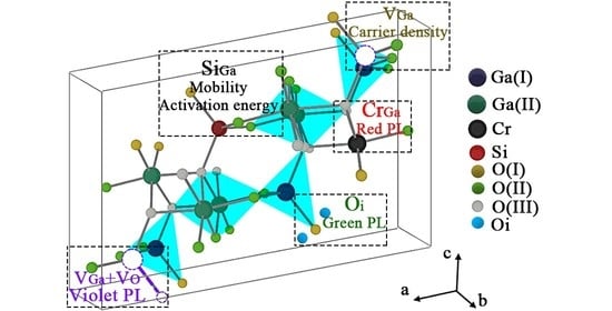
3. Results and Discussion

As shown in Figure 1a, three sharp XRD peaks appear for the diffraction on the (-201), ( 4 ¯ 02), and ( 6 ¯ 03) planes of β-Ga2O3. For further comparison, the ( 2 ¯ 01) diffraction peak and the full width at half maximum (FWHM) were selected and investigated, as shown in Figure 1b,c. According to the intensity of the (-201) plane, the computed texture coefficients for the unannealed, vac-annealed, and O2-annealed samples were 0.91, 0.87, and 0.76 (detailed calculations are provided in the supplementary information). Each sample was measured several times to minimize possible fluctuations. The average FWHM of the ( 2 ¯ 01) diffraction peak was 44.2 arcsec for the pristine sample, which reduced to the average value of 38.3 arcsec due to vacuum annealing. The reduced FWHM indicates an improvement in bulk crystallinity, and the resultant dislocation density decreased from 3.1 × 10⁴ to 2.3 × 104 cm−3 as extracted from the FWHMs [20,21]. However, although the FWHM of the O2-annealed sample (44.6 arcsec) was similar to that of the control sample, an obvious shoulder peak appeared (Figure 1b: red line), which was attributed to the strain accumulation induced by the diffusion of Si and Cr impurities toward the surface (detailed discussion provided in the SIMS section).
The Raman spectra of the samples are presented in Figure 2a [22]. According to the calculation of the factor group analysis at the Γ point [23], 27 optical phonon modes exist as Γopt = 10Ag + 5Bg + 4Au + 8Bu, among which Ag and Bg are Raman active, whereas Au and Bu are infrared active [24]. Although the Raman mode intensity can be affected by the crystal orientation and surface content of the vibrating group [23], the information on the latter is believed to be dominantly reflected by the Raman measurements because the crystal orientation and test conditions of the samples are completely consistent. All peaks are normalized via calibration based on the Si substrate. Compared to the pristine sample, the Raman peaks that vary predominantly for the annealed samples are listed in Figure 2b. Although the Bg(5) mode is believed to be dependent only on Ga(I) and O(III) [25], its weakness for the O2-annealed sample implies the reduction in Ga(I) instead of in O(III) because the concentration of O(III) is difficult to drop in an oxygen-rich ambience due to the large energy formation (Ef) of VO(III) around 4.7 eV [11]. As a result, the weakened Bg(5) strongly suggests an increase in Ga-related vacancies with reduced Ga(I) concentration. On the other hand, the strengthened Bg(5) mode of the vacuum-annealed sample demonstrates an increased O(III) concentration, which results from the recovery with Oi point defects, as discussed later. Additionally, Raman modes other than the Bg(5) mode are related to at least three types of atoms [25], which makes it difficult to provide solid evidence.
The SIMS measurement is used and corrected to identify the residual impurity compositions in the pristine, vac-annealed, and O2-annealed Ga2O3, demonstrating the existence of Si and Cr impurities, the former of which is the main residual impurity, as shown in Figure 3a. According to the SIMS measurement, the normalized concentrations of impurities are extracted from all the samples, in which the relative values of Cr+, Si+, and Ga+ are 1/176/385,987, 1/80/2936, and 1/303/31,665 for the unannealed, O2-annealed, and vac-annealed samples, respectively. For the vac-annealed sample (Figure 3b), the Ga concentration near the surface is almost unchanged, but the Si and Cr concentrations are higher than that of the pristine sample, which indicates that annealing can promote the residual Si and Cr out-diffusion toward the surface. In Figure 3c, it can be seen that the Ga concentration near the surface of the O2-annealed sample is lower than that of the pristine and vac-annealed samples, which indicates the formation of VGa near the surface caused by O2 annealing [26]. In addition, the increasing content of Si and Cr impurities near the surface of the O2-annealed sample strongly indicates the migration of Si and Cr impurities toward the surface by O2 annealing, which can occupy the VGa to promote the formations of SiGa and CrGa. The migration of Si and Cr impurities toward the surface leads to the accumulation of strain [26], which induces a shoulder peak in the corresponding XRD pattern (Figure 1b). The SEM images of the surface morphologies of all three samples are shown in the SI. Figure 2 shows the degraded surface of the O2-annealed sample.
Figure 4a presents the room-temperature PL spectra of the pristine, oxygen-annealed, vacuum-annealed, and (vacuum+oxygen)-annealed samples. The spectral peaks centered at 408 nm (3.04 eV) and 508 nm (2.44 eV) can be observed for all samples, although their intensities significantly subside for both vacuum and oxygen annealing. According to the calculation by Quoc et al., the defects of VGa+VO and Oi are located at ~3.0 eV and ~2.4 eV below the conduction band minimum (CBM) to act as deep acceptors (detailed calculated defect levels are shown in Supplementary Figure S1) [11,27]. During the PL measurement, electrons trapped by these acceptors rather than in the valence band are believed to be excited in the conduction band because the 325 nm excitation photos have lower energy than the bandgap of Ga2O3. These excited electrons transit to the near-CBM energy levels of the Si shallow donor via non-irradiative processes and subsequently drop to the deep acceptors to generate violet and green luminescence, which are related to the defects of VGa+VO and Oi, respectively [11]. Therefore, the weakened violet and green PL peaks for the annealed samples reflect the reduction in both defects, which result from the enhanced combination of intrinsic Oi and the divacancy VGa+VO by absorbing thermal energy during annealing. Notably, the green PL peak is less weakened for the oxygen-annealed sample than for the vacuum-annealed sample because ambient oxygen (25 sccm) can be absorbed to compensate for VGa+VO so that fewer intrinsic Oi is consumed.
Interestingly, a broadband red PL peak centered at 716 nm is observed only for the sample annealed in O2, which is associated with a spike peak (690 nm) on its shoulder (Figure 4b). An additional pristine sample is sequentially annealed in a vacuum and oxygen ambience to verify the existence of the red PL peak, which also appears (Figure 4a: green line). Although the defects of V O ( I I I ) 0 are located at 1.7 eV below the conduction band, which corresponds to a wavelength of around 716 nm [11], it should not be the origin of the red PL peak because VO is difficult to form in oxygen ambience due to its high formation energy of 4.7 eV [10,11]. Furthermore, the broad red PL peak can be attributed to the electron transitions from the 4T2 and 2E states to the 4A2 levels of the Cr3+ impurities [28,29,30,31,32], which are generated by recharging Cr2+ during thermal annealing to shift the Fermi level away from the conduction band [21,22]. As for the spike peak at 690 nm, the transition of the 2E:R2 states to ground 4A2 is believed to be the dominant origin [18,33,34].
Temperature-dependent Hall measurements were conducted to further explore the annealing effects. As shown in Figure 5a, the electron mobility of the three samples in this study is comparable at 300 K, which is 100 cm2/V·s, and is in good agreement with previous studies [10,35]. The carrier mobility was mainly determined using lattice vibration scattering and ionized impurity scattering, which can be expressed as exponents T−1.5 and T1.5, respectively [36]. The closest exponent to the theoretical T−1.5 for the vacuum-annealed sample suggests its improved crystallinity to enhance lattice vibration scattering, as supported by the reduction in both Oi and VGa+VO defects (the fitting process is shown in Supplementary Table S1).
At 200 K (1000/T3/2 ≈ 0.35), the oxygen-annealed sample shows higher mobility than the pristine Ga2O3, whereas the vacuum-annealed sample is lower because annealing in oxygen increases the amount of defective VGa to provide more sites for Si and Cr impurities. Consequently, substitutions of SiGa and CrGa are formed, thus weakening the impurity scattering for carrier mobility improvement. On the other hand, annealing in a vacuum repels Si and Cr from the lattice to enhance ionized impurity scattering, which is dominant at this temperature [33].
The carrier concentration and activation energy of Si-doped Ga2O3 are listed in Table 1. Our results are in good agreement with those of the previous studies. As shown in Figure 5b, the free carrier density slightly decreases for both the samples annealed in vacuum and O2 at 300 K, although acceptor-like VGa+VO and Oi defects are simultaneously passivated by annealing. This reduction in carrier density might be caused by the increase in VGa originating from the recovery of VGa+VO and Oi in bulk Ga2O3 [10]. The VGa can act as electron traps to capture electrons, thus pushing the Fermi level away from the conduction band to reduce the carrier density [10,37,38,39].
Based on the plot of carrier density versus temperature, the thermal activation energies of the carriers for all samples are extracted using the following Arrhenius equation (see, Figure 5b) [42]:
N = n 0 exp ( - E a kT )
where k is the Boltzmann constant (1.38 × 10⁻²³ J/K), T is the temperature, N is the electron density measured at T, Ea is the activation energy, and n0 is the pre-exponential factor.
The extracted activation energy shows a 16.8 meV for the pristine sample and increases to 21.8 meV for the vacuum-annealed sample. This is caused by the diffusion of Si impurities toward the surface to generate interstitial Si (Sii) [43], which can behave as donors with an activation energy of 150 meV, as reported by Assil et al. [16], thus increasing the activation energy. On the other hand, although the impurities also diffuse in the oxygen-annealed sample, its activation energy decreases to 15.6 meV because the amount of VGa in oxygen can be increased to provide more sites for occupation by the diffused Si, producing SiGa as primary shallow donors to reduce the activation energy [12,13,14]. Interestingly, with different activation energies, the carrier concentration is approximately at room temperature for both annealed samples because more VGa are formed in the oxygen-annealed sample, behaving as deep acceptor traps to capture electron carriers.
Furthermore, the curves in Figure 5b for the oxygen- and vacuum-annealed samples intersect at around 300 K, indicating comparable carrier densities. In the region of low temperature, the carrier density of the oxygen-annealed sample is higher, which results from its lower activation energy to excite more carriers, as discussed above. Interestingly, its carrier density is lower than that of the vacuum-annealed sample at high temperatures, which originates from the recovery between VGa+VO and Oi, as reflected in Figure 4a, where more oxygen interstitials remain in the oxygen ambience.

4. Conclusions

In conclusion, the effects of annealing on surface residual impurities (Si and Cr) and intrinsic defects in bulk UID Ga2O3 were identified and investigated. It was found that the recovery between divacancies VGa+VO and interstitials (Oi) occured during annealing, which improved the crystal quality. Using Raman and PL measurements, the diffusion of residual impurities toward the surface was observed. Interestingly, an extra red PL peak appeared only for the oxygen-annealed sample, which was attributed to the existence of Cr3+ impurities, as depicted by SIMS. Moreover, the carrier mobility was improved by oxygen annealing because it could produce more VGa near the surface to incorporate the diffused Si and Cr impurities to form substitutions of SiGa and CrGa, thereby weakening the impurity scattering. Finally, the carrier density of the oxygen-annealed sample was found to be higher than that of the vacuum-annealed sample at low temperatures because the former has a lower impurity activation energy, whereas the result was the opposite at high temperatures due to the recovery between VGa+VO and Oi. In short, studying the behaviors of these defects can help us to better understand and regulate the optical and electrical properties of Ga2O3.

Supplementary Materials

The following supporting information can be downloaded at: https://www.mdpi.com/article/10.3390/cryst13071045/s1, Figure S1: The calculated various intrinsic defects and a substitutional No by Ho in [11]; Figure S2: The SEM images of the unannealed, Vac-annealed, and O2-annealed samples; Table S1: The fitted data of mobility [44,45].

Author Contributions

Writing—original draft preparation, S.W.; software, Z.L.; formal analysis, H.Y.; writing—review and editing, Y.W. All authors have read and agreed to the published version of the manuscript.

Funding

This study was supported by the National Natural Science Foundation of China (grant number 62101044).

Data Availability Statement

The data that support the findings of this study are available from the corresponding author upon reasonable request.

Conflicts of Interest

The authors declare no conflict of interest.

References

  1. Goyal, P.; Kaur, H. Implementing variable doping and work function engineering in β-Ga2O3 MOSFET to realize high breakdown voltage and PfoM. Semicond. Sci. Technol. 2022, 37, 045018. [Google Scholar] [CrossRef]
  2. Xu, S.; Liu, L.; Qu, G.; Zhang, X.; Jia, C.; Wu, S.; Ma, Y.; Lee, Y.J.; Wang, G.; Park, J.-H.; et al. Single β-Ga2O3 nanowire based lateral FinFET on Si. Appl. Phys. Lett. 2022, 120, 153501. [Google Scholar] [CrossRef]
  3. Qu, G.; Xu, S.; Liu, L.; Tang, M.; Wu, S.; Jia, C.; Zhang, X.; Song, W.; Lee, Y.J.; Xu, J.; et al. Single β-Ga2O3 nanowire back-gate field-effect transistor. Semicond. Sci. Technol. 2022, 37, 085009. [Google Scholar] [CrossRef]
  4. Joishi, C.; Rafique, S.; Xia, Z.; Han, L.; Krishnamoorthy, S.; Zhang, Y.; Lodha, S.; Zhao, H.; Rajan, S. Low-pressure CVD-grown β-Ga2O3 bevel-field-plated Schottky barrier diodes. Appl. Phys. Express 2018, 11, 031101. [Google Scholar] [CrossRef] [Green Version]
  5. Higashiwaki, M. β-Gallium Oxide Devices: Progress and Outlook. Phys. Status Solidi Rapid Res. Lett. 2021, 15, 2100357. [Google Scholar] [CrossRef]
  6. Tao, X. Bulk gallium oxide single crystal growth. J. Semicond. 2019, 40, 010401. [Google Scholar] [CrossRef]
  7. Usseinov, A.; Koishybayeva, Z.; Platonenko, A.; Pankratov, V.; Suchikova, Y.; Akilbekov, A.; Zdorovets, M.; Purans, J.; Popov, A.I. Vacancy Defects in Ga2O3: First-Principles Calculations of Electronic Structure. Materials 2021, 14, 7384. [Google Scholar] [CrossRef]
  8. Kananen, B.E.; Giles, N.C.; Halliburton, L.E.; Foundos, G.K.; Chang, K.B.; Stevens, K.T. Self-trapped holes in β-Ga2O3 crystals. J. Appl. Phys. 2017, 122, 215703. [Google Scholar] [CrossRef]
  9. Kananen, B.E.; Halliburton, L.E.; Stevens, K.T.; Foundos, G.K.; Giles, N.C. Gallium vacancies in β-Ga2O3 crystals. Appl. Phys. Lett. 2017, 110, 202104. [Google Scholar] [CrossRef]
  10. McCluskey, M.D. Point defects in Ga2O3. J. Appl. Phys. 2020, 127, 101101. [Google Scholar] [CrossRef] [Green Version]
  11. Ho, Q.D.; Frauenheim, T.; Deák, P. Origin of photoluminescence in β-Ga2O3. Phys. Rev. B 2018, 97, 115163. [Google Scholar] [CrossRef]
  12. Son, N.T.; Goto, K.; Nomura, K.; Thieu, Q.T.; Togashi, R.; Murakami, H.; Kumagai, Y.; Kuramata, A.; Higashiwaki, M.; Koukitu, A.; et al. Electronic properties of the residual donor in unintentionally doped β-Ga2O3. J. Appl. Phys. 2016, 120, 235703. [Google Scholar] [CrossRef] [Green Version]
  13. Rafique, S.; Han, L.; Neal, A.T.; Mou, S.; Tadjer, M.J.; French, R.H.; Zhao, H. Heteroepitaxy of N-type β-Ga2O3 thin films on sapphire substrate by low pressure chemical vapor deposition. Appl. Phys. Lett. 2016, 109, 132103. [Google Scholar] [CrossRef] [Green Version]
  14. Feng, Z.; Anhar Uddin Bhuiyan, A.F.M.; Karim, M.R.; Zhao, H. MOCVD homoepitaxy of Si-doped (010) β-Ga2O3 thin films with superior transport properties. Appl. Phys. Lett. 2019, 114, 250601. [Google Scholar] [CrossRef]
  15. Varley, J.B.; Weber, J.R.; Janotti, A.; Van de Walle, C.G. Oxygen vacancies and donor impurities in β-Ga2O3. Appl. Phys. Lett. 2010, 97, 142106. [Google Scholar] [CrossRef]
  16. Bouzid, A.; Pasquarello, A. Defect Formation Energies of Interstitial C, Si, and Ge Impurities in β-Ga2O3. Phys. Status Solidi Rapid Res. Lett. 2019, 13, 1800633. [Google Scholar] [CrossRef]
  17. Neal, A.T.; Mou, S.; Lopez, R.; Li, J.V.; Thomson, D.B.; Chabak, K.D.; Jessen, G.H. Incomplete Ionization of a 110 meV Unintentional Donor in beta-Ga2O3 and its Effect on Power Devices. Sci. Rep. 2017, 7, 13218. [Google Scholar] [CrossRef] [Green Version]
  18. Luchechko, A.; Vasyltsiv, V.; Zhydachevskyy, Y.; Kushlyk, M.; Ubizskii, S.; Suchocki, A. Luminescence spectroscopy of Cr3+ ions in bulk single crystalline β-Ga2O3. J. Phys. D 2020, 53, 354001. [Google Scholar] [CrossRef]
  19. Luchechko, A.; Vasyltsiv, V.; Kostyk, L.; Tsvetkova, O.; Pavlyk, B. The Effect of Cr3+ and Mg2+ Impurities on Thermoluminescence and Deep Traps in β-Ga2O3 Crystals. ECS J. Solid State Sci. Technol. 2020, 9, 045008. [Google Scholar] [CrossRef]
  20. Aida, H.; Nishiguchi, K.; Takeda, H.; Aota, N.; Sunakawa, K.; Yaguchi, Y. Growth of β-Ga2O3 Single Crystals by the Edge-Defined, Film Fed Growth Method. Jpn. J. Appl. Phys. 2008, 47, 8506. [Google Scholar] [CrossRef]
  21. Bae, H.; Lee, K.-S.; Ye, P.D.; Park, J.-Y. Current annealing to improve drain output performance of β-Ga2O3 field-effect transistor. Solid State Electron. 2021, 185, 108134. [Google Scholar] [CrossRef]
  22. Zhang, K.; Xu, Z.; Zhang, S.; Wang, H.; Cheng, H.; Hao, J.; Wu, J.; Fang, F. Raman and photoluminescence properties of un-/ion-doped β-Ga2O3 single-crystals prepared by edge-defined film-fed growth method. Phys. B Condens. Matter 2021, 600, 412624. [Google Scholar] [CrossRef]
  23. Kranert, C.; Sturm, C.; Schmidt-Grund, R.; Grundmann, M. Raman tensor elements of beta-Ga2O3. Sci. Rep. 2016, 6, 35964. [Google Scholar] [CrossRef] [PubMed] [Green Version]
  24. Dohy, D.; Lucazeau, G.; Revcolevschi, A. Raman spectra and valence force field of single-crystalline β-Ga2O3. J. Solid State Chem. 1982, 45, 180. [Google Scholar] [CrossRef]
  25. Janzen, B.M.; Mazzolini, P.; Gillen, R.; Falkenstein, A.; Martin, M.; Tornatzky, H.; Maultzsch, J.; Bierwagen, O.; Wagner, M.R. Isotopic study of Raman active phonon modes in β-Ga2O3. J. Mater. Chem. C 2021, 9, 2311. [Google Scholar] [CrossRef]
  26. Azarov, A.; Venkatachalapathy, V.; Vines, L.; Monakhov, E.; Lee, I.-H.; Kuznetsov, A. Activation energy of silicon diffusion in gallium oxide: Roles of the mediating defects charge states and phase modification. Appl. Phys. Lett. 2021, 119, 182103. [Google Scholar] [CrossRef]
  27. Onuma, T.; Fujioka, S.; Yamaguchi, T.; Higashiwaki, M.; Sasaki, K.; Masui, T.; Honda, T. Correlation between blue luminescence intensity and resistivity in β-Ga2O3 single crystals. Appl. Phys. Lett. 2013, 103, 041910. [Google Scholar] [CrossRef] [Green Version]
  28. Stehr, J.E.; Jansson, M.; Hofmann, D.M.; Kim, J.; Pearton, S.J.; Chen, W.M.; Buyanova, I.A. Magneto-optical properties of Cr3+ in β-Ga2O3. Appl. Phys. Lett. 2021, 119, 052101. [Google Scholar] [CrossRef]
  29. Sun, R.; Ooi, Y.K.; Dickens, P.T.; Lynn, K.G.; Scarpulla, M.A. On the origin of red luminescence from iron-doped β-Ga2O3 bulk crystals. Appl. Phys. Lett. 2020, 117, 052101. [Google Scholar] [CrossRef]
  30. Nogales, E.; Garcia, J.A.; Mendez, B.; Piqueras, J. Red luminescence of Cr in beta-Ga2O3 nanowires. J. Appl. Phys. 2007, 101, 033517. [Google Scholar] [CrossRef] [Green Version]
  31. Wang, C.; Qiao, X.; Fan, X. Research Progress on Blue LED Excited Cr3+ Doped Phosphors with Broad-band Near-infrared Luminescence. Chin. J. Lumin. 2022, 43, 1855–1870. [Google Scholar] [CrossRef]
  32. Zhang, J.; Zhang, L.; Ren, J.; Duan, P.; Luo, Y.; Lv, S. Properties of NIR Emissions with Energy-transfer Processes in Cr3+-and Yb3+-doped Y3Al5O12 Powder Materials. Chin. J. Lumin. 2015, 36, 0262–0266. [Google Scholar] [CrossRef]
  33. Vasyltsiv, V.; Luchechko, A.; Zhydachevskyy, Y.; Kostyk, L.; Lys, R.; Slobodzyan, D.; Jakieła, R.; Pavlyk, B.; Suchocki, A. Correlation between electrical conductivity and luminescence properties in β-Ga2O3:Cr3+ and β-Ga2O3:Cr, Mg single crystals. J. Vac. Sci. Technol. A 2021, 39, 033201. [Google Scholar] [CrossRef]
  34. Tokida, Y.; Adachi, S. Photoluminescence spectroscopy and energy-level analysis of metal-organic-deposited Ga2O3:Cr3+ films. Jpn. J. Appl. Phys. 2012, 112, 063522. [Google Scholar] [CrossRef]
  35. Labed, M.; Sengouga, N.; Labed, M.; Meftah, A.; Kyoung, S.; Kim, H.; Rim, Y.S. Modeling and analyzing temperature-dependent parameters of Ni/β-Ga2O3 Schottky barrier diode deposited by confined magnetic field-based sputtering. Semicond. Sci. Technol. 2021, 36, 035020. [Google Scholar] [CrossRef]
  36. Irmscher, K.; Galazka, Z.; Pietsch, M.; Uecker, R.; Fornari, R. Electrical properties of β-Ga2O3 single crystals grown by the Czochralski method. J. Appl. Phys. 2011, 110, 063720. [Google Scholar] [CrossRef]
  37. Cui, H.; Sai, Q.; Qi, H.; Zhao, J.; Si, J.; Pan, M. Analysis on the electronic trap of β-Ga2O3 single crystal. J. Mater. Sci. 2019, 54, 12643. [Google Scholar] [CrossRef]
  38. Galazka, Z. Growth of bulk β-Ga2O3 single crystals by the Czochralski method. J. Appl. Phys. 2022, 131, 031103. [Google Scholar] [CrossRef]
  39. Sasaki, K.; Higashiwaki, M.; Kuramata, A.; Masui, T.; Yamakoshi, S. Si-Ion Implantation Doping in β-Ga2O3 and Its Application to Fabrication of Low-Resistance Ohmic Contacts. Appl. Phys. Express 2013, 6, 086502. [Google Scholar] [CrossRef]
  40. Goto, K.; Konishi, K.; Murakami, H.; Kumagai, Y.; Monemar, B.; Higashiwaki, M.; Kuramata, A.; Yamakoshi, S. Halide vapor phase epitaxy of Si doped β-Ga2O3 and its electrical properties. Thin Solid Films 2018, 666, 182–184. [Google Scholar] [CrossRef]
  41. Rajapitamahuni, A.K.; Thoutam, L.R.; Ranga, P.; Krishnamoorthy, S.; Jalan, B. Impurity band conduction in Si-doped β-Ga2O3 films. Appl. Phys. Lett. 2021, 118, 072105. [Google Scholar] [CrossRef]
  42. Li, J.V.; Johnston, S.W.; Yan, Y.; Levi, D.H. Measuring temperature-dependent activation energy in thermally activated processes: A 2D Arrhenius plot method. Rev. Sci. Instrum. 2010, 81, 033910. [Google Scholar] [CrossRef] [PubMed] [Green Version]
  43. Sharma, R.; Law, M.E.; Fares, C.; Tadjer, M.; Ren, F.; Kuramata, A.; Pearton, S.J. The role of annealing ambient on diffusion of implanted Si in beta-Ga2O3. AIP Adv. 2019, 9, 085111. [Google Scholar] [CrossRef] [Green Version]
  44. Mohamed, S.H.; El-Hagary, M.; Althoyaib, S. Growth of β-Ga2O3 nanowires and their photocatalytic and optical properties using Pt as a catalyst. J. Alloys Compd. 2012, 537, 291–296. [Google Scholar] [CrossRef]
  45. Wang, Y.; Tang, W.; Zhang, L. Crystalline Size Effects on Texture Coefficient, Electrical and Optical Properties of Sputter-deposited Ga-doped ZnO Thin Films. J. Mater. Sci. Technol. 2015, 31, 175–181. [Google Scholar] [CrossRef]
Figure 1. XRD measurement results for the three types of Ga2O3. (a) The 2-theta scan of the unannealed Ga2O3. (b,c) The ( 2 ¯ 01) plane rocking curves of all samples.
Crystals 13 01045 g001
Figure 2. (a) Raman shift of three types of Ga2O3 from 150 to 800 cm−1. (b) The peaks varying predominantly for annealed samples are listed.
Crystals 13 01045 g002
Figure 3. The in-depth SIMS profile of Ga, Si, and Cr for the (a) unannealed, (b) vac-annealed, and (c) O2-annealed Ga2O3.
Crystals 13 01045 g003
Figure 4. (a) PL spectra at an arbitrary scale for the four crystal types. (b) Magnified red PL spectrum of Ga2O3 annealed in O2 from 650 nm to 800 nm. (c) PL mechanism in Ga2O3: violet, green, and red emissions.
Crystals 13 01045 g004
Figure 5. The temperature-dependent (a) electron mobility and (b) carrier density for the three types of bulk Ga2O3.
Crystals 13 01045 g005
Table 1. The carrier density and activation energy of Si-doped Ga2O3.
Si-Doped Ga2O3Carrier Density (E17)Activation Energy (meV)References
film13.210.1[13]
film0.27534.9[14]
film0.145.6[40]
film7.833.7–45.6[41]
bulk0.75110[17]
bulk~1015–17[12]
this work4.5–5.015.6–21.8
Disclaimer/Publisher’s Note: The statements, opinions and data contained in all publications are solely those of the individual author(s) and contributor(s) and not of MDPI and/or the editor(s). MDPI and/or the editor(s) disclaim responsibility for any injury to people or property resulting from any ideas, methods, instructions or products referred to in the content.

