Article

Virtual Work Principle for Piezoelectric Semiconductors and Its Application on Extension and Bending of ZnO Nanowires

1
Unmanned Vehicle Innovation Center, Ningbo Institute of NPU, Ningbo 315048, China
2
Jiangsu Key Laboratory of Engineering Mechanics, School of Civil Engineering, Southeast University, Nanjing 210096, China
3
School of Science, Xi’an University of Architecture and Technology, Xi’an 710055, China
4
School of Marine Science and Technology, Northwestern Polytechnical University, Xi’an 710072, China
*
Authors to whom correspondence should be addressed.
Crystals 2023, 13(9), 1368; https://doi.org/10.3390/cryst13091368
Submission received: 15 August 2023 / Revised: 4 September 2023 / Accepted: 8 September 2023 / Published: 12 September 2023

Abstract

:
This paper presents the principle of virtual work (PVW) for piezoelectric semiconductors (PSs), which extends the piezoelectric dielectrics to involve the semiconducting effect. As an application of the PVW, a one-dimensional (1D) approximation theory for the extension and bending of PS nanowires is established by directly applying the PVW and Bernoulli–Euler beam theory with the aid of the second-order approximation of electrostatic potential. To illustrate the new model, the mechanical displacement, electrostatic potential, and concentration of electrons for extension and bending deformation of n-type ZnO nanowires are analytically determined. Additionally, numerical results show that, for n-type Zinc Oxide nanowires, the distribution of electrostatic potential is anti-symmetric along the thickness direction for extension deformation. In contrast, the bending deformation causes a symmetric distribution of electrostatic potential characterized by the zeroth-order and the second-order electrostatic potential. Furthermore, these two different deformations result in the redistribution of electrons. The electrostatic potential can be tuned by adjusting the amplitude of the applied mechanical load. Moreover, we find that the increase in doping level will reduce the magnitude of electrostatic potential due to the screening effect. The presented PVW provides a general approach to establishing structural theories and an effective way of implementing numerical methods.

1. Introduction

Piezoelectric semiconductors (PSs) are materials with both semiconducting and piezoelectric properties [1], whose crystal structure usually belongs to group III-V zinc-blende (e.g., GaAs) and group II-VI wurtzite (e.g., ZnO). In PSs, stress/strain produces electric polarization through piezoelectric coupling, thereby resulting in the redistribution of free carriers. As early as the 1960s, researchers made their efforts on the application of PSs on acoustoelectric devices. Meanwhile, bulk acoustic waves, delay lines, traveling wave amplifiers, and oscillators were developed [2]. The research of piezoelectric semiconductor materials and devices encountered rapid development in the early twenty-first century. Various one-dimensional (1D) and two-dimensional (2D) structures of PSs, including fibers, spirals, belts, and films [3,4,5], have been synthesized using modern material processing techniques. These PS structures have a broad application in energy harvesting, sensing, transduction, and electronics. Studies on PS structures have formed new and rapidly developing research fields called piezotronics and piezo-phototronics [6]. Based on the piezotronics effect, Wang et al. [7] proposed a nanogenerator by using zinc oxide nanowire arrays and achieved the conversion between mechanical energy and electrical energy.
The development of PSs has generated significant interest among researchers in the field of mechanics, leading to extensive theoretical investigations. For example, Sharma et al. [8] studied the surface waves in a PS composite structure. Tian et al. [9] investigated the characteristics of elastic waves propagating in an anisotropic n-type PSs plate. Cao et al. [10] investigated the generalized Rayleigh surface waves in a PS half space. Gokhale and Rais-Zadeh [11] studied the vibrations of acoustic wave resonators. Sladek et al. [12] investigated a dynamic analysis of an anti-plane crack in PSs. Fan et al. [13] proposed a piezoelectric-conductor iterative method for the analysis of cracks in PSs. Qin et al. [14] investigated the fracture behavior of GaN PS ceramics under combined mechanical and electric loading. In addition, the PS rods [15,16,17,18], beams [19,20], plates [21,22,23], PN junction [24], and Schottky junction [25] were analyzed. Recently, Qu et al. [26] proposed a continuum theory for analyzing the interaction between the thermoelectric and mechanical fields in PSs. In addition, nanowires made from Zinc Oxide typically exhibit slender structures (they typically have diameters of 20–100 nm and lengths of a few micrometers [27]). As a result, they are often approximated as a Bernoulli–Euler beam. Researchers have conducted extensive studies on the application of the Bernoulli–Euler beam theory to PSs. For example, Liang et al. [28] developed a 1D static buckling model for PSs. Zhang et al. [29] proposed a 1D multi-field coupling model incorporating surface effects for PS nanostructures based on surface elasticity theory. Zhang et al. [30] investigated the dynamic buckling and free bending vibration of an axially compressed simply supported PS rod. Luo et al. [31] studied the bending of a composite fiber of piezoelectric dielectrics and nonpiezoelectric semiconductors.
The aforementioned models are constructed by using differential methods. It is noted that using differential methods to derive field equations and boundary conditions is ambiguous and difficult in dealing with higher-order structural theories. The principle of virtual work (PVW) is another method for developing structural theories that allows for the simultaneous derivation of field equations and boundary conditions more simply and conveniently [32,33,34]. The PVW offers a crucial framework employed for deriving solutions in mechanics, electrostatics, and so on, serving as the foundation for the finite element method. Using the PVW, researchers investigate structures like beams and plates. For example, Falsone and La Valle [35] used the PVW to derive the field equations of functionally graded beams subjected to axial and transversal loads. Ascione et al. [36] derived the nonlinear equilibrium equations of geometrically imperfect composite beams based on the PVW.
The objective of this work is to propose the PVW for PSs and analyze the electric behavior of the PS nanowires when axial and transverse loadings are applied. The rest of the paper is arranged as follows: In Section 2, the three-dimensional (3-D) framework for PSs is established, including formulations for PVW and constitutive relations. In Section 3, the field equations for PS nanowires and corresponding boundary conditions are derived with the aid of the PVW and the Bernoulli–Euler beam theory which consider the second-order approximation of electrostatic potential. In addition, the 1-D constitutive relations are obtained by taking into account the stress relaxation procedure. Finally, the governing equations of PS nanowires are derived. In Section 4, as the application, the extension and bending for ZnO nanowires are explored. The concluding remarks are given in Section 5.

2. Three-Dimensional Framework for PSs

2.1. The PVW for PSs

The field equations and corresponding boundary conditions for PSs can be derived from the following PVW:
δ 𝕎 ( d ) + δ 𝕎 ( c ) + δ 𝕎 ( i ) = 0 ,
where δ𝕎(d), δ𝕎(c), and δ𝕎(i) represent the virtual work of actions at a distance, contact forces, and internal forces [37], as
δ 𝕎 ( d ) = Ω [ ( f i ρ u ¨ i ) δ u i q ( p n + N D + N A ) δ φ + λ q ( p ˙ δ p n ˙ δ n ) ] d v ,
δ 𝕎 ( c ) = Ω [ ( t i δ u i ) + ( ω δ φ ) + λ ( J p δ p + J n δ n ) ] d A ,
δ 𝕎 ( i ) = Ω [ T i j δ S i j D i δ E i + λ ( J i p δ P i + J i n δ N i ) ] d v ,
where Ω is the region occupied by PSs; dv is the volume element; fi is the mechanical body force; ρ is the mass density; ui is mechanical displacement; q is the elementary charge; p and n are the concentrations of holes and electrons; N D + and N A are the concentrations of ionized donors and acceptors; φ is electrostatic potential; λ is a constant with a unit J·m6·s·C−1, which satisfies all terms associated with concentrations of free-carriers having units J; ti, ω, Jp, and Jn are surface traction, surface charge, and surface electric currents for holes and electrons, respectively; Tij, Di, J i p and J i n are Cauchy stress, electric displacement, electric current densities for holes and electrons, respectively; and Sij, Ei, Pi, and Ni are the strain, electric field, gradient of concentration of holes and electrons.
In addition, Sij, Ei, Pi, and Ni are related to ui, φ, p, and n through
S i j = ( u i , j + u j , i ) / 2 , E i = φ , i , P i = p , i , N i = n , i .
It is noted that Equation (1) is a weak form for differential equations of semiconducting systems with elastic considerations. Due to the dissipation nature (the first-order time derivative of concentrations), no functionals can be obtained, and δ𝕎 represents a symbol of virtual work rather than variation of 𝕎.

2.2. Constitutive Relations for PSs

The constitutive relations (for Cauchy stress Tij, electric displacement Di, electric current densities for holes and electrons, J i p and J i n ) of PSs read [21]:
T i j = c i j k l S k l e k i j E k ,
D i = ε i j E j + e i j k S j k ,
J i p = q p μ i j p E j q D i j p P j ,
J i n = q n μ i j n E j + q D i j n N j ,
where cijkl, eijk, and εij are, respectively, the elastic stiffness constants, piezoelectric constants, and dielectric constants; μ i j p and μ i j n are, respectively, the carrier mobilities for holes and electrons; and D i j p and D i j n are, respectively, the carrier diffusion constants for holes and electrons.
Concentration perturbations for holes and electrons can be expressed as:
Δ p = p p 0 , Δ n = n n 0 , p 0 = N A , n 0 = N D + ,
where p0 and n0 denote doping level. For the case of small Δp and Δn, the constitutive relations (8) and (9) can be linearized into
J i p q p 0 μ i j p E j q D i j p P j , J i n q n 0 μ i j n E j + q D i j n N j .

3. One-Dimensional Model for PS Nanowires

3.1. Field Equations for PS Nanowires

Consider a PS nanowire as shown in Figure 1. The length of PS nanowires is L, which is along the x1 direction. The width and height of PS nanowires are, respectively, 2b and 2h. The surface traction ti, surface charge ω, and surface electric currents for holes and electrons Jp and Jn are not considered here. Note that although this paper primarily discusses nanowires with rectangular cross-sections, it is also applicable to circular, elliptical, and other cross-sectional shapes.
With the aid of the Bernoulli–Euler beam theory, the displacements of PS nanowires [38] can be given by
u 1 ( x , t ) u 1 ( 0 ) ( x 1 , t ) x 3 u 3 , 1 ( 0 ) ( x 1 , t ) , u 2 ( x , t ) = 0 , u 3 ( x , t ) u 3 ( 0 ) ( x 1 , t ) ,
where u 1 ( 0 ) describes the in-plane extensional displacement and u 3 ( 0 ) represents the bending displacement.
Moreover, the second-order approximation of electrostatic potential, the concentration of holes and electrons can be given by [39]
φ ( x , t ) φ ( 0 ) ( x 1 , t ) + x 3 φ ( 1 ) ( x 1 , t ) + ( x 3 2 h 2 ) φ ( 2 ) ( x 1 , t ) , p ( x , t ) p ( 0 ) ( x 1 , t ) + x 3 p ( 1 ) ( x 1 , t ) + ( x 3 2 h 2 ) p ( 2 ) ( x 1 , t ) , n ( x , t ) n ( 0 ) ( x 1 , t ) + x 3 n ( 1 ) ( x 1 , t ) + ( x 3 2 h 2 ) n ( 2 ) ( x 1 , t ) ,
where φ ( 0 ) , φ ( 1 ) , and φ ( 2 ) are, respectively, the zeroth-, first-, and second-order electrostatic potentials. Similarly, p ( 0 ) ( n ( 0 ) ), p ( 1 ) ( n ( 1 ) ), and p ( 2 ) ( n ( 2 ) ) are the zeroth-, first-, and second-order holes (electrons) concentration.
Inserting Equations (12) and (13) into Equation (5), we have the nonzero components of strain, electrostatic potential, and gradient of concentration of holes and electrons:
S 11 = u 1 , 1 ( 0 ) x 3 u 3 , 11 ( 0 ) ,
E 1 = [ φ , 1 ( 0 ) + x 3 φ , 1 ( 1 ) + ( x 3 2 h 2 ) φ , 1 ( 2 ) ] , E 3 = ( φ ( 1 ) + 2 x 3 φ ( 2 ) ) ,
P 1 = p , 1 ( 0 ) + x 3 p , 1 ( 1 ) + ( x 3 2 h 2 ) p , 1 ( 2 ) , P 3 = p ( 1 ) + 2 x 3 p ( 2 ) , N 1 = n , 1 ( 0 ) + x 3 n , 1 ( 1 ) + ( x 3 2 h 2 ) n , 1 ( 2 ) , N 3 = n ( 1 ) + 2 x 3 n ( 2 ) .
Substituting Equations (12) and (13) into Equation (2), the virtual work of actions at a distance yields
δ 𝕎 ( d ) = 0 L [ ( f 1 ( 0 ) ρ ( 0 ) u ¨ 1 ( 0 ) ) δ u 1 ( 0 ) ( f 3 ( 0 ) + f 1 , 1 ( 1 ) ρ ( 0 ) u ¨ 3 ( 0 ) + ρ ( 2 ) u ¨ 3 , 11 ( 0 ) ) δ u 3 ( 0 ) + ( q ( 0 ) p ( 0 ) + q ( 2 ) p ( 2 ) q ( 0 ) n ( 0 ) q ( 2 ) n ( 2 ) + q ( 0 ) N D + q ( 0 ) N A ) δ φ ( 0 ) + ( q ˜ ( 2 ) p ( 1 ) q ˜ ( 2 ) n ( 1 ) ) δ φ ( 1 ) + ( q ( 2 ) p ( 0 ) + q ( 4 ) p ( 2 ) q ( 2 ) n ( 0 ) q ( 4 ) n ( 2 ) + q ( 2 ) N D + q ( 2 ) N A ) δ φ ( 2 ) λ ( q ( 0 ) p ˙ ( 0 ) + q ( 2 ) p ˙ ( 2 ) ) δ p ( 0 ) λ q ˜ ( 2 ) p ˙ ( 1 ) δ p ( 1 ) λ ( q ( 2 ) p ˙ ( 0 ) + q ( 4 ) p ˙ ( 2 ) ) δ p ( 2 ) + λ ( q ( 0 ) n ˙ ( 0 ) + q ( 2 ) n ˙ ( 2 ) ) δ n ( 0 ) + λ q ˜ ( 2 ) n ˙ ( 1 ) δ n ( 1 ) + λ ( q ( 2 ) n ˙ ( 0 ) + q ( 4 ) n ˙ ( 2 ) ) δ n ( 2 ) ] d x 1 + [ ( f 1 ( 1 ) + ρ ( 2 ) u ¨ 3 , 1 ( 0 ) ) δ u 3 ( 0 ) ] 0 L ,
where
{ q ( 0 ) , q ˜ ( 2 ) } = 2 b h h { q , q x 3 2 } d x 3 = { I ( 0 ) , I ( 2 ) } q , { ρ ( 0 ) , ρ ( 2 ) } = 2 b h h { ρ , ρ x 3 2 } d x 3 = { I ( 0 ) , I ( 2 ) } ρ , q ( 2 ) = 2 b h h q ( x 3 2 h 2 ) d x 3 = 2 I ( 2 ) q , q ( 4 ) = 2 b h h q ( x 3 2 h 2 ) 2 d x 3 = I ( 4 ) q , I ( 0 ) = 4 b h , I ( 2 ) = 4 b h 3 3 , I ( 4 ) = 32 b h 5 15 ,
and the resultants of external body force over a cross-section are defined by:
{ f 1 ( 0 ) , f 3 ( 0 ) , f 1 ( 1 ) } = 2 b h h { f 1 , f 3 , f 1 x 3 } d x 3 .
Substituting Equations (14)–(16) into Equation (4), the virtual work of internal forces yields
δ 𝕎 ( i ) = 0 L { T 11 , 1 ( 0 ) δ u 1 ( 0 ) T 11 , 11 ( 1 ) δ u 3 ( 0 ) D 1 , 1 ( 0 ) δ φ ( 0 ) + ( D 3 ( 0 ) D 1 , 1 ( 1 ) ) δ φ ( 1 ) + ( 2 D 3 ( 1 ) D 1 , 1 ( 2 ) ) δ φ ( 2 ) + λ [ J 1 , 1 p ( 0 ) δ p ( 0 ) + ( J 3 p ( 0 ) J 1 , 1 p ( 1 ) ) δ p ( 1 ) + ( 2 J 3 p ( 1 ) J 1 , 1 p ( 2 ) ) δ p ( 2 ) ] + λ [ J 1 , 1 n ( 0 ) δ n ( 0 ) + ( J 3 n ( 0 ) J 1 , 1 n ( 1 ) ) δ n ( 1 ) + ( 2 J 3 n ( 1 ) J 1 , 1 n ( 2 ) ) δ n ( 2 ) ] } d x 1 + [ T 11 ( 0 ) δ u 1 ( 0 ) ] 0 L [ T 11 ( 1 ) δ u 3 , 1 ( 0 ) ] 0 L + [ T 11 , 1 ( 1 ) δ u 3 ( 0 ) ] 0 L + [ D 1 ( 0 ) δ φ ( 0 ) ] 0 L + [ D 1 ( 1 ) δ φ ( 1 ) ] 0 L + [ D 1 ( 2 ) δ φ ( 2 ) ] 0 L + [ λ J 1 p ( 0 ) δ p ( 0 ) ] 0 L + [ λ J 1 p ( 1 ) δ p ( 1 ) ] 0 L + [ λ J 1 p ( 2 ) δ p ( 2 ) ] 0 L + [ λ J 1 n ( 0 ) δ n ( 0 ) ] 0 L + [ λ J 1 n ( 1 ) δ n ( 1 ) ] 0 L + [ λ J 1 n ( 2 ) δ n ( 2 ) ] 0 L ,
where the resultants of stress, electric displacement, and electric current densities for holes and electrons are defined as:
{ T 11 ( 0 ) , T 11 ( 1 ) } = 2 b h h { T 11 , T 11 x 3 } d x 3 ,
{ D 1 ( 0 ) , D 3 ( 0 ) , D 1 ( 1 ) , D 3 ( 1 ) } = 2 b h h { D 1 , D 3 , D 1 x 3 , D 3 x 3 } d x 3 , D 1 ( 2 ) = 2 b h h [ D 1 ( x 3 2 h 2 ) ] d x 3 ,
{ J 1 p ( 0 ) , J 3 p ( 0 ) , J 1 p ( 1 ) , J 3 p ( 1 ) } = 2 b h h { J 1 p , J 3 p , J 1 p x 3 , J 3 p x 3 } d x 3 , J 1 p ( 2 ) = 2 b h h [ J 1 p ( x 3 2 h 2 ) ] d x 3 , { J 1 n ( 0 ) , J 3 n ( 0 ) , J 1 n ( 1 ) , J 3 n ( 1 ) } = 2 b h h { J 1 n , J 3 n , J 1 n x 3 , J 3 n x 3 } d x 3 , J 1 n ( 2 ) = 2 b h h [ J 1 n ( x 3 2 h 2 ) ] d x 3 .
Substituting Equations (17) and (20) into Equation (1) then leads to, with the aid of the fundamental lemma of the calculus of variation [40,41],
T 11 , 1 ( 0 ) + f 1 ( 0 ) = ρ ( 0 ) u ¨ 1 ( 0 ) , T 11 , 11 ( 1 ) + f 1 , 1 ( 1 ) + f 3 ( 0 ) = ρ ( 0 ) u ¨ 3 ( 0 ) ρ ( 2 ) u ¨ 3 , 11 ( 0 ) , D 1 , 1 ( 0 ) = q ( 0 ) ( p ( 0 ) n ( 0 ) + N D + N A ) + q ( 2 ) ( p ( 2 ) n ( 2 ) ) , D 1 , 1 ( 1 ) D 3 ( 0 ) = q ˜ ( 2 ) ( p ( 1 ) n ( 1 ) ) , D 1 , 1 ( 2 ) 2 D 3 ( 1 ) = q ( 2 ) ( p ( 0 ) n ( 0 ) + N D + N A ) + q ( 4 ) ( p ( 2 ) n ( 2 ) ) , J 1 , 1 p ( 0 ) = q ( 0 ) p ˙ ( 0 ) q ( 2 ) p ˙ ( 2 ) , J 1 , 1 n ( 0 ) = q ( 0 ) n ˙ ( 0 ) + q ( 2 ) n ˙ ( 2 ) , J 1 , 1 p ( 1 ) J 3 p ( 0 ) = q ˜ ( 2 ) p ˙ ( 1 ) , J 1 , 1 n ( 1 ) J 3 n ( 0 ) = q ˜ ( 2 ) n ˙ ( 1 ) , J 1 , 1 p ( 2 ) 2 J 3 p ( 1 ) = q ( 2 ) p ˙ ( 0 ) q ( 4 ) p ˙ ( 2 ) , J 1 , 1 n ( 2 ) 2 J 3 n ( 1 ) = q ( 2 ) n ˙ ( 0 ) + q ( 4 ) n ˙ ( 2 ) ,
as the field equations, and
T 11 ( 0 ) = 0 or u 1 ( 0 ) = u ¯ 1 ( 0 ) , T 11 ( 1 ) = 0 or u 3 , 1 ( 0 ) = u ¯ 3 , 1 ( 0 ) , T 11 , 1 ( 1 ) + f 1 ( 1 ) = 0 or u 3 ( 0 ) = u ¯ 3 ( 0 ) , D 1 ( 0 ) = 0 or φ ( 0 ) = φ ¯ ( 0 ) , D 1 ( 1 ) = 0 or φ ( 1 ) = φ ¯ ( 1 ) , D 1 ( 2 ) = 0 or φ ( 2 ) = φ ¯ ( 2 ) , J 1 p ( 0 ) = 0 or p ( 0 ) = p ¯ ( 0 ) , J 1 p ( 1 ) = 0 or p ( 1 ) = p ¯ ( 1 ) , J 1 p ( 2 ) = 0 or p ( 2 ) = p ¯ ( 2 ) , J 1 n ( 0 ) = 0 or n ( 0 ) = n ¯ ( 0 ) , J 1 n ( 1 ) = 0 or n ( 1 ) = n ¯ ( 1 ) , J 1 n ( 2 ) = 0 or n ( 2 ) = n ¯ ( 2 ) ,
as the boundary conditions for x1 = 0 or L.

3.2. One-Dimensional Constitutive Relations

Consider a PS nanowire with 6mm class crystals that poles along the x3 direction [21,26], then the constitutive relations Equations (6), (7), and (11) become
T 11 = c 11 S 11 + c 12 S 22 + c 13 S 33 e 31 E 3 , T 22 = c 12 S 11 + c 11 S 22 + c 13 S 33 e 31 E 3 , T 33 = c 13 S 11 + c 13 S 22 + c 33 S 33 e 33 E 3 ,
D 1 = ε 11 E 1 , D 3 = ε 33 E 3 + e 31 S 11 + e 31 S 22 + e 33 S 33 ,
J 1 p q p 0 μ 11 p E 1 q D 11 p P 1 , J 3 p q p 0 μ 33 p E 3 q D 33 p P 3 ,
J 1 n q n 0 μ 11 n E 1 + q D 11 n N 1 , J 3 n q n 0 μ 33 n E 3 + q D 33 n N 3 .
Consider the stress relaxation procedure with T22 = T33 = 0 [42], it derives
S 22 = c 12 c 33 c 13 2 c 11 c 33 c 13 2 S 11 c 13 e 33 c 33 e 31 c 11 c 33 c 13 2 E 3 , S 33 = c 12 c 13 c 11 c 13 c 11 c 33 c 13 2 S 11 + c 11 e 33 c 13 e 31 c 11 c 33 c 13 2 E 3 .
Inserting Equation (30) into Equations (26)–(29) and with the help of Equations (14)–(16), we have
T 11 = c ¯ 11 u 1 , 1 ( 0 ) c ¯ 11 x 3 u 3 , 11 ( 0 ) + e ¯ 31 φ ( 1 ) + 2 e ¯ 31 x 3 φ ( 2 ) ,
D 1 = ε 11 φ , 1 ( 0 ) ε 11 x 3 φ , 1 ( 1 ) ε 11 ( x 3 2 h 2 ) φ , 1 ( 2 ) , D 3 = ε ¯ 33 φ ( 1 ) 2 ε ¯ 33 x 3 φ ( 2 ) + e ¯ 31 u 1 , 1 ( 0 ) e ¯ 31 x 3 u 3 , 11 ( 0 ) ,
J 1 p q p 0 μ 11 p [ φ , 1 ( 0 ) + x 3 φ , 1 ( 1 ) + ( x 3 2 h 2 ) φ , 1 ( 2 ) ] q D 11 p [ p , 1 ( 0 ) + x 3 p , 1 ( 1 ) + ( x 3 2 h 2 ) p , 1 ( 2 ) ] , J 3 p q p 0 μ 33 p ( φ ( 1 ) + 2 x 3 φ ( 2 ) ) q D 33 p ( p ( 1 ) + 2 x 3 p ( 2 ) ) ,
J 1 n q n 0 μ 11 n [ φ , 1 ( 0 ) + x 3 φ , 1 ( 1 ) + ( x 3 2 h 2 ) φ , 1 ( 2 ) ] + q D 11 n [ n , 1 ( 0 ) + x 3 n , 1 ( 1 ) + ( x 3 2 h 2 ) n , 1 ( 2 ) ] , J 3 n q n 0 μ 33 n ( φ ( 1 ) + 2 x 3 φ ( 2 ) ) + q D 33 n ( n ( 1 ) + 2 x 3 n ( 2 ) ) ,
where the effective material constants are defined as:
c ¯ 11 = c 11 + 2 c 12 c 13 2 c 33 c 12 2 c 11 c 13 2 c 11 c 33 c 13 2 , e ¯ 31 = e 31 + ( c 12 c 11 ) c 13 e 33 + ( c 13 2 c 12 c 33 ) e 31 c 11 c 33 c 13 2 , ε ¯ 33 = ε 33 + c 11 e 33 2 2 c 13 e 31 e 33 + c 33 e 31 2 c 11 c 33 c 13 2 .
According to Equations (21)–(23) and (31)–(34), the correct 1-D constitutive relations can be given by
T 11 ( 0 ) = c ¯ 11 ( 0 ) u 1 , 1 ( 0 ) + e ¯ 31 ( 0 ) φ ( 1 ) , T 11 ( 1 ) = c ¯ 11 ( 2 ) u 3 , 11 ( 0 ) + 2 e ¯ 31 ( 2 ) φ ( 2 ) ,
D 1 ( 0 ) = ε 11 ( 0 ) φ , 1 ( 0 ) + 2 ε 11 ( 2 ) φ , 1 ( 2 ) , D 3 ( 0 ) = ε ¯ 33 ( 0 ) φ ( 1 ) + e ¯ 31 ( 0 ) u 1 , 1 ( 0 ) , D 1 ( 1 ) = ε 11 ( 2 ) φ , 1 ( 1 ) , D 3 ( 1 ) = 2 ε ¯ 33 ( 2 ) φ ( 2 ) e ¯ 31 ( 2 ) u 3 , 11 ( 0 ) , D 1 ( 2 ) = 2 ε 11 ( 2 ) φ , 1 ( 0 ) ε 11 ( 4 ) φ , 1 ( 2 ) ,
J 1 p ( 0 ) = μ 11 p ( 0 ) φ , 1 ( 0 ) D 11 p ( 0 ) p , 1 ( 0 ) + 2 μ 11 p ( 2 ) φ , 1 ( 2 ) + 2 D 11 p ( 2 ) p , 1 ( 2 ) , J 3 p ( 0 ) = μ 33 p ( 0 ) φ ( 1 ) D 33 p ( 0 ) p ( 1 ) , J 1 p ( 1 ) = μ 11 p ( 2 ) φ , 1 ( 1 ) D 11 p ( 2 ) p , 1 ( 1 ) , J 3 p ( 1 ) = 2 μ 33 p ( 2 ) φ ( 2 ) 2 D 33 p ( 2 ) p ( 2 ) , J 1 p ( 2 ) = 2 μ 11 p ( 2 ) φ , 1 ( 0 ) + 2 D 11 p ( 2 ) p , 1 ( 0 ) μ 11 p ( 4 ) φ , 1 ( 2 ) D 11 p ( 4 ) p , 1 ( 2 ) ,
J 1 n ( 0 ) = μ 11 n ( 0 ) φ , 1 ( 0 ) + D 11 n ( 0 ) n , 1 ( 0 ) + 2 μ 11 n ( 2 ) φ , 1 ( 2 ) 2 D 11 n ( 2 ) n , 1 ( 2 ) , J 3 n ( 0 ) = μ 33 n ( 0 ) φ ( 1 ) + D 33 n ( 0 ) n ( 1 ) , J 1 n ( 1 ) = μ 11 n ( 2 ) φ , 1 ( 1 ) + D 11 n ( 2 ) n , 1 ( 1 ) , J 3 n ( 1 ) = 2 μ 33 n ( 2 ) φ ( 2 ) + 2 D 33 n ( 2 ) n ( 2 ) , J 1 n ( 2 ) = 2 μ 11 n ( 2 ) φ , 1 ( 0 ) 2 D 11 n ( 2 ) n , 1 ( 0 ) μ 11 n ( 4 ) φ , 1 ( 2 ) + D 11 n ( 4 ) n , 1 ( 2 ) ,
where
{ c ¯ 11 ( m ) , ε 11 ( m ) , ε ¯ 33 ( m ) , e ¯ 31 ( m ) , μ 11 p ( m ) , D 11 p ( m ) , μ 33 p ( m ) , D 33 p ( m ) , μ 11 n ( m ) , D 11 n ( m ) , μ 33 n ( m ) , D 33 n ( m ) } = 2 b h h { c ¯ 11 , ε 11 , ε ¯ 33 , e ¯ 31 , q p 0 μ 11 p , q D 11 p , q p 0 μ 33 p , q D 33 p , q n 0 μ 11 n , q D 11 n , q n 0 μ 33 n , q D 33 n } x 3 m d x 3 , m = 0 , 2 , 4 .
The substitution of Equations (36)–(39) into Equation (24) yields the governing equations of PS nanowires, which can be decoupled into two groups,
c ¯ 11 ( 0 ) u 1 , 11 ( 0 ) + e ¯ 31 ( 0 ) φ , 1 ( 1 ) + f 1 ( 0 ) = ρ ( 0 ) u ¨ 1 ( 0 ) , ε 11 ( 2 ) φ , 11 ( 1 ) e ¯ 31 ( 0 ) u 1 , 1 ( 0 ) + ε ¯ 33 ( 0 ) φ ( 1 ) = q ˜ ( 2 ) ( p ( 1 ) n ( 1 ) ) , μ 11 p ( 2 ) φ , 11 ( 1 ) D 11 p ( 2 ) p , 11 ( 1 ) + μ 33 p ( 0 ) φ ( 1 ) + D 33 p ( 0 ) p ( 1 ) = q ˜ ( 2 ) p ˙ ( 1 ) , μ 11 n ( 2 ) φ , 11 ( 1 ) + D 11 n ( 2 ) n , 11 ( 1 ) + μ 33 n ( 0 ) φ ( 1 ) D 33 n ( 0 ) n ( 1 ) = q ˜ ( 2 ) n ˙ ( 1 ) ,
and
c ¯ 11 ( 2 ) u 3 , 1111 ( 0 ) + 2 e ¯ 31 ( 2 ) φ , 11 ( 2 ) + f 1 , 1 ( 1 ) + f 3 ( 0 ) = ρ ( 0 ) u ¨ 3 ( 0 ) ρ ( 2 ) u ¨ 3 , 11 ( 0 ) , ε 11 ( 0 ) φ , 11 ( 0 ) + 2 ε 11 ( 2 ) φ , 11 ( 2 ) = q ( 0 ) ( p ( 0 ) n ( 0 ) + N D + N A ) + q ( 2 ) ( p ( 2 ) n ( 2 ) ) , 2 ε 11 ( 2 ) φ , 11 ( 0 ) ε 11 ( 4 ) φ , 11 ( 2 ) + 2 e ¯ 31 ( 2 ) u 3 , 11 ( 0 ) + 4 ε ¯ 33 ( 2 ) φ ( 2 ) = q ( 2 ) ( p ( 0 ) n ( 0 ) + N D + N A ) + q ( 4 ) ( p ( 2 ) n ( 2 ) ) , μ 11 p ( 0 ) φ , 11 ( 0 ) D 11 p ( 0 ) p , 11 ( 0 ) + 2 μ 11 p ( 2 ) φ , 11 ( 2 ) + 2 D 11 p ( 2 ) p , 11 ( 2 ) = q ( 0 ) p ˙ ( 0 ) q ( 2 ) p ˙ ( 2 ) , μ 11 n ( 0 ) φ , 11 ( 0 ) + D 11 n ( 0 ) n , 11 ( 0 ) + 2 μ 11 n ( 2 ) φ , 11 ( 2 ) 2 D 11 n ( 2 ) n , 11 ( 2 ) = q ( 0 ) n ˙ ( 0 ) + q ( 2 ) n ˙ ( 2 ) , 2 μ 11 p ( 2 ) φ , 11 ( 0 ) + 2 D 11 p ( 2 ) p , 11 ( 0 ) μ 11 p ( 4 ) φ , 11 ( 2 ) D 11 p ( 4 ) p , 11 ( 2 ) + 4 μ 33 p ( 2 ) φ ( 2 ) + 4 D 33 p ( 2 ) p ( 2 ) = q ( 2 ) p ˙ ( 0 ) q ( 4 ) p ˙ ( 2 ) , 2 μ 11 n ( 2 ) φ , 11 ( 0 ) 2 D 11 n ( 2 ) n , 11 ( 0 ) μ 11 n ( 4 ) φ , 11 ( 2 ) + D 11 n ( 4 ) n , 11 ( 2 ) + 4 μ 33 n ( 2 ) φ ( 2 ) 4 D 33 n ( 2 ) n ( 2 ) = q ( 2 ) n ˙ ( 0 ) + q ( 4 ) n ˙ ( 2 ) .
Equation (41) describes the extensional motion of PS nanowires. Specifically, extension deformation u 1 ( 0 ) is coupled with φ ( 1 ) , p ( 1 ) , and n ( 1 ) . Equation (42) shows the bending motion of PS nanowires, in which the bending deformation u 3 ( 0 ) is coupled with φ ( 0 ) , φ ( 2 ) , p ( 0 ) , p ( 2 ) , n ( 0 ) , and n ( 2 ) .

4. Examples

4.1. Extension of ZnO Nanowires

As an application of Equation (41), consider the extension of the ZnO nanowires subjected to an axial load. The semiconductor is of n-type with p0 = 0 and Δp = 0. The uniform doping is adopted here. All terms related to time and holes will be omitted in Equation (27) later.
The boundary conditions of ZnO nanowires are Ohmic contacts at x1 = 0 and L, namely,
T 11 ( 0 ) = 0 , φ ( 1 ) = 0 , n ( 1 ) = 0 .
The axial load with amplitude T0 along the x1 direction can be written as:
f 1 ( 0 ) = T 0 cos ( π x 1 L ) .
Let the Navier solutions that satisfy boundary conditions Equation (43) be:
{ φ ( 1 ) , n ( 1 ) } = m = 1 { Φ m ( 1 ) , N m ( 1 ) } sin ( ξ m x 1 ) , { u 1 ( 0 ) , f 1 ( 0 ) } = m = 1 { U m ( 0 ) , T m ( 0 ) } cos ( ξ m x 1 ) , ξ m = m π L , m = 1 , 2 , 3
where Φ m ( 1 ) , N m ( 1 ) , and U m ( 0 ) are the undetermined Fourier coefficients. The Fourier coefficient T m ( 0 ) is given by [43]:
T 1 ( 0 ) = T 0 , T m ( 0 ) = 0 ( m 1 ) .
Substituting Equation (45) into Equation (41), and noticing that there exist nontrivial solutions only when m = 1, we have:
𝕂 11 𝕂 12 0 𝕂 12 𝕂 22 𝕂 23 0 𝕂 32 𝕂 33 U 1 ( 0 ) Φ 1 ( 1 ) N 1 ( 1 ) = T 1 ( 0 ) 0 0 ,
where
𝕂 11 = c ¯ 11 ( 0 ) ( π L ) 2 , 𝕂 12 = e ¯ 31 ( 0 ) π L , 𝕂 22 = ε 11 ( 2 ) ( π L ) 2 + ε ¯ 33 ( 0 ) , 𝕂 23 = q ˜ ( 2 ) , 𝕂 32 = μ 11 n ( 2 ) ( π L ) 2 + μ 33 n ( 0 ) , 𝕂 33 = [ D 11 n ( 2 ) ( π L ) 2 + D 33 n ( 0 ) ] .
Solving the linear algebraic equation system in Equation (47) will yield the Fourier coefficients:
U 1 ( 0 ) = L 2 T 0 π 2 [ c ¯ 11 ( 0 ) + ( e ¯ 31 ( 0 ) ) 2 ε ¯ 33 ( 0 ) + ε 11 ( 2 ) ( π 2 L 2 + 1 λ D 2 ) ] , Φ 1 ( 1 ) = L e ¯ 31 ( 0 ) T 0 π { ( e ¯ 31 ( 0 ) ) 2 + c ¯ 11 ( 0 ) [ ε ¯ 33 ( 0 ) + ε 11 ( 2 ) ( π 2 L 2 + 1 λ D 2 ) ] } , N 1 ( 1 ) = q n 0 L e ¯ 31 ( 0 ) T 0 k B T π { ( e ¯ 31 ( 0 ) ) 2 + c ¯ 11 ( 0 ) [ ε ¯ 33 ( 0 ) + ε 11 ( 2 ) ( π 2 L 2 + 1 λ D 2 ) ] } ,
where the Debye–Hückel length of charge systems λD is defined as
λ D = ε 11 k B T q 2 n 0 .
Additionally, the Einstein relation is utilized in deriving Equation (49), i.e.,
μ 11 D 11 = q k B T ,
where kB is the Boltzmann constant and T is absolute temperature.
According to Equations (12), (13), (45), and (49), the displacement field u1, electrostatic potential φ, and the concentration of electrons n reads:
u 1 = L 2 T 0 π 2 [ c ¯ 11 ( 0 ) + ( e ¯ 31 ( 0 ) ) 2 ε ¯ 33 ( 0 ) + ε 11 ( 2 ) ( π 2 L 2 + 1 λ D 2 ) ] cos ( π L x 1 ) ,
φ = L e ¯ 31 ( 0 ) T 0 π { ( e ¯ 31 ( 0 ) ) 2 + c ¯ 11 ( 0 ) [ ε ¯ 33 ( 0 ) + ε 11 ( 2 ) ( π 2 L 2 + 1 λ D 2 ) ] } x 3 sin ( π L x 1 ) ,
n = n 0 q n 0 L e ¯ 31 ( 0 ) T 0 k B T π { ( e ¯ 31 ( 0 ) ) 2 + c ¯ 11 ( 0 ) [ ε ¯ 33 ( 0 ) + ε 11 ( 2 ) ( π 2 L 2 + 1 λ D 2 ) ] } x 3 sin ( π L x 1 ) .
From Equation (52), it is observed that the displacement u1 increases with the increase of the doping level (i.e., λ D decrease with the increase of n 0 , lead to the increase of u 1 ). It is seen that the extension displacement is always greater than that of piezoelectric dielectric, as a result of semiconducting effect.
From Equation (53), the electrostatic potential decreases with the increase of doping level n0, i.e., the increase doping level n0 causes the decrease of λ D and leads to the decrease of the electrostatic potential. This indicates that electrons have a screening effect on the electrostatic potential induced by the piezoelectric effect. Furthermore, for a high doping level with n 0 , λ D 0 , we have φ = 0 . This indicates that the electrostatic potential induced by the piezoelectric effect is totally screened, and the PS turns into a conductor.
Particularly, when the semiconducting effect is not considered, we have n 0 = 0 and λ D . The current PS nanowires reduce to that for piezoelectric dielectric, and the corresponding solutions are
u 1 = L 2 T 0 π 2 [ c ¯ 11 ( 0 ) + L 2 ( e ¯ 31 ( 0 ) ) 2 L 2 ε ¯ 33 ( 0 ) + π 2 ε 11 ( 2 ) ] cos ( π L x 1 ) ,
φ = L 3 e ¯ 31 ( 0 ) T 0 π [ L 2 ( e ¯ 31 ( 0 ) ) 2 + c ¯ 11 ( 0 ) ( L 2 ε ¯ 33 ( 0 ) + π 2 ε 11 ( 2 ) ) ] x 3 sin ( π L x 1 ) .
To further investigate the solution in the current model, a numerical example is taken into account. The material properties of ZnO nanowires are shown as follows [1]:
c 11 = c 22 = 209.7   GPa , c 33 = 210.9   GPa , c 12 = 121.1   GPa , c 13 = c 23 = 105.1   GPa , c 44 = 42.47   GPa , e 31 = 0.573   C / m 2 , e 33 = 1.32   C / m 2 , ε 11 = 8.1 × 10 11 C / ( V m ) , ε 33 = 1.12 × 10 10 C / ( V m ) .
The electron mobilities are from Sze and Ng [44]: μ 11 n = μ 33 n = 200 × 10 4   m 2 / ( V s ) . The diffusion constants are D 11 n = D 33 n = 4.6575 × 10 4   m 2 / s . Moreover, the elementary charge and doping level are q = 1.602 × 10⁻¹⁹ C and n0 = 1 × 10²¹ m−3. The Boltzmann constant is 1.381 × 10⁻²³ J/K and the absolute temperature takes 300 K. The sizes of ZnO nanowires are L = 600 nm, b = 50 nm, and h = 30 nm, respectively. In addition, the amplitude T0 of the axial load is 0.1 N/m.
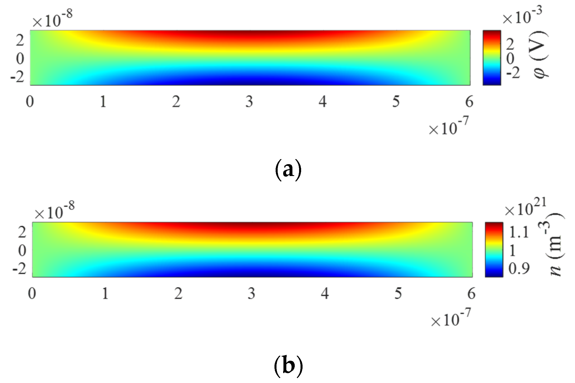
From Figure 2a, it indicates that the top of ZnO nanowires has a high electrostatic potential while the bottom has a low potential. The total potential is distributed anti-symmetrically along the x3 direction. Figure 2b indicates that the electrons are redistributed under extension deformation. The electrons move toward the top of the ZnO nanowires where they become negative charges, leaving the bottom half of the nanowire positive charges.
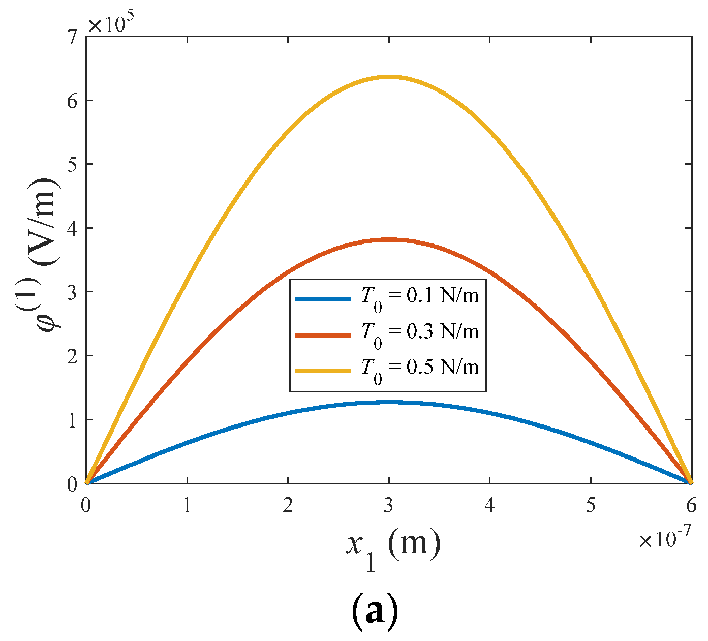
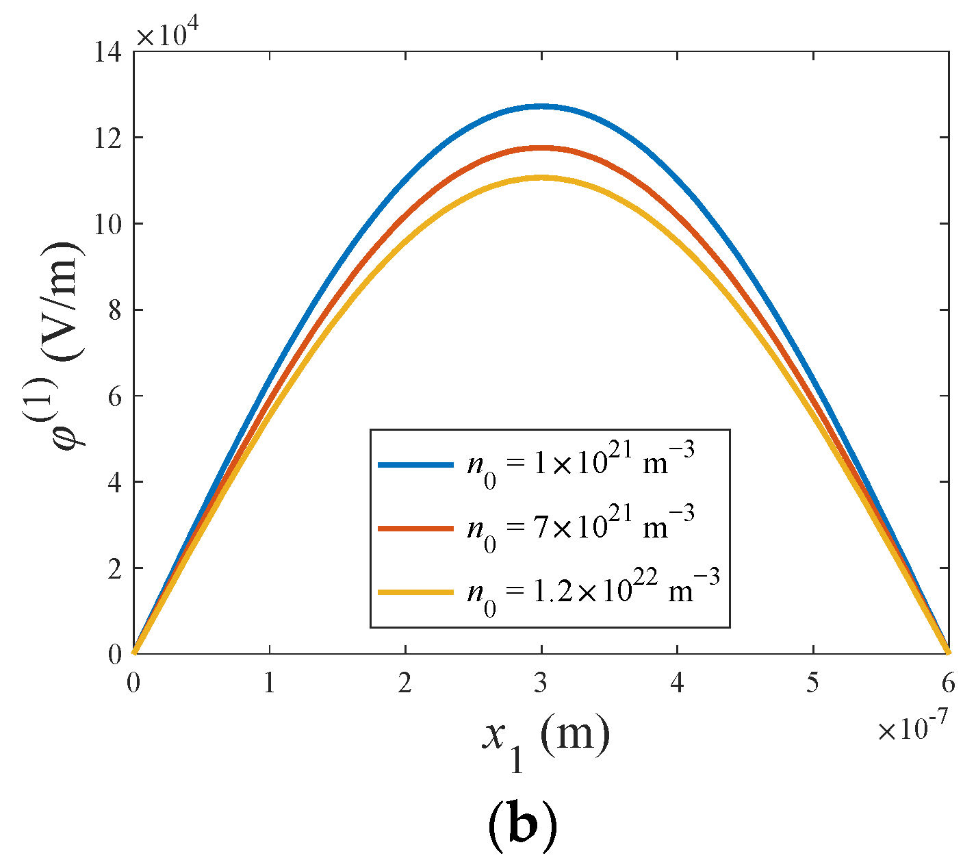
To further illustrate the effects of the amplitude of axial load and doping level, the electrostatic potential varying with x1 of ZnO nanowires is plotted in Figure 3a,b. From Figure 3a, it can be seen that the electrostatic potential shows an enhancement with the increase in mechanical load amplitude. Moreover, the increased doping level lead to a depressed electrostatic potential (see Figure 3b). Driven by mechanically induced polarization, the electrons move to screen the effective polarization charges and thus lower the magnitude of the first-order electrostatic potential [45]; this is consistent with the earlier discussion. It can be predicted that the first-order electrostatic potential φ ( 1 ) reaches its maximum value when the semiconducting effect vanishes.

4.2. Bending of ZnO Nanowires

As an application of Equation (42), consider the bending of ZnO nanowires subjected to a transverse load. The semiconductor is of n-type and uniform doping is adopted here. Introduce Δ n ( 0 ) = n ( 0 ) n 0 , the governing equations for bending of ZnO nanowires can be given by omitting the items related to time and holes,
c ¯ 11 ( 2 ) u 3 , 1111 ( 0 ) + 2 e ¯ 31 ( 2 ) φ , 11 ( 2 ) + f 3 ( 0 ) = 0 , ε 11 ( 0 ) φ , 11 ( 0 ) + 2 ε 11 ( 2 ) φ , 11 ( 2 ) = q ( 0 ) Δ n ( 0 ) q ( 2 ) n ( 2 ) , 2 ε 11 ( 2 ) φ , 11 ( 0 ) ε 11 ( 4 ) φ , 11 ( 2 ) + 2 e ¯ 31 ( 2 ) u 3 , 11 ( 0 ) + 4 ε ¯ 33 ( 2 ) φ ( 2 ) = q ( 2 ) Δ n ( 0 ) q ( 4 ) n ( 2 ) , μ 11 n ( 0 ) φ , 11 ( 0 ) + D 11 n ( 0 ) Δ n , 11 ( 0 ) + 2 μ 11 n ( 2 ) φ , 11 ( 2 ) 2 D 11 n ( 2 ) n , 11 ( 2 ) = 0 , 2 μ 11 n ( 2 ) φ , 11 ( 0 ) 2 D 11 n ( 2 ) Δ n , 11 ( 0 ) μ 11 n ( 4 ) φ , 11 ( 2 ) + D 11 n ( 4 ) n , 11 ( 2 ) + 4 μ 33 n ( 2 ) φ ( 2 ) 4 D 33 n ( 2 ) n ( 2 ) = 0 .
For boundary conditions, Ohmic contacts at x1 = 0 and L are assumed, namely
T 11 ( 1 ) = 0 , u 3 ( 0 ) = 0 , φ ( 0 ) = 0 , φ ( 2 ) = 0 , Δ n ( 0 ) = 0 , n ( 2 ) = 0 . at x 1 = 0 , L .
Equation (59)5,6 indicate n = n 0 at the x1 = 0 and L, which satisfies the acquirement of Ohmic contacts.
Consider the Navier solutions of the following Fourier series form:
{ u 3 ( 0 ) , φ ( 0 ) , φ ( 2 ) , Δ n ( 0 ) , n ( 2 ) , f 3 ( 0 ) } = m = 1 { W m ( 0 ) , Φ m ( 0 ) , Φ m ( 2 ) , N m ( 0 ) , N m ( 2 ) , F m ( 0 ) } sin ( ξ m x 1 ) , ξ m = m π L , m = 1 , 2 , 3
where W m ( 0 ) , Φ m ( 0 ) , Φ m ( 2 ) , N m ( 0 ) , and N m ( 2 ) are the undetermined Fourier coefficients; F m ( 0 ) is the known Fourier coefficient. Notably, Equation (60) satisfies the boundary conditions (59).
The transverse load with amplitude F0 can be written as:
f 3 ( 0 ) = F 0 sin ( π x 1 L ) ,
thus the Fourier coefficient of f 3 ( 0 ) is [46]:
F 1 ( 0 ) = F 0 , F m ( 0 ) = 0 ( m 1 ) .
Using Equations (60) and (62) into Equation (58), and noticing that there exist nontrivial solutions only when m = 1, we have:
𝕄 11 0 𝕄 13 0 0 0 𝕄 22 𝕄 23 𝕄 24 𝕄 25 𝕄 13 𝕄 23 𝕄 33 𝕄 25 𝕄 35 0 𝕄 42 𝕄 43 𝕄 44 𝕄 45 0 𝕄 43 𝕄 53 𝕄 45 𝕄 55 W 1 ( 0 ) Φ 1 ( 0 ) Φ 1 ( 2 ) N 1 ( 0 ) N 1 ( 2 ) = F 1 ( 0 ) 0 0 0 0 ,
where the nonzero components of coefficients matrices are
𝕄 11 = c ¯ 11 ( 2 ) ( π L ) 4 , 𝕄 13 = 2 e ¯ 31 ( 2 ) ( π L ) 2 , 𝕄 22 = ε 11 ( 0 ) ( π L ) 2 , 𝕄 23 = 2 ε 11 ( 2 ) ( π L ) 2 , 𝕄 24 = q ( 0 ) , 𝕄 25 = q ( 2 ) , 𝕄 33 = ε 11 ( 4 ) ( π L ) 2 + 4 ε ¯ 33 ( 2 ) , 𝕄 35 = q ( 4 ) , 𝕄 42 = μ 11 n ( 0 ) ( π L ) 2 , 𝕄 43 = 2 μ 11 n ( 2 ) ( π L ) 2 , 𝕄 44 = D 11 n ( 0 ) ( π L ) 2 , 𝕄 45 = 2 D 11 n ( 2 ) ( π L ) 2 , 𝕄 53 = μ 11 n ( 4 ) ( π L ) 2 + 4 μ 33 n ( 2 ) , 𝕄 55 = [ D 11 n ( 4 ) ( π L ) 2 + 4 D 33 n ( 2 ) ] .
Solving the linear algebraic equation system in Equation (63) will yield the Fourier coefficients as,
W 1 ( 0 ) = L 4 F 0 π 4 [ c ¯ 11 ( 2 ) + 4 ( e ¯ 31 ( 2 ) ) 2 4 ε ¯ 33 ( 2 ) + ( ε 11 ( 4 ) 4 I ( 2 ) I ( 0 ) ε 11 ( 2 ) ) ( π 2 L 2 + 1 λ D 2 ) ] , Φ 1 ( 0 ) = 4 L 2 I ( 2 ) e ¯ 31 ( 2 ) F 0 π 2 I ( 0 ) { 4 ( e ¯ 31 ( 2 ) ) 2 + c ¯ 11 ( 2 ) [ 4 ε ¯ 33 ( 2 ) + ( ε 11 ( 4 ) 4 I ( 2 ) I ( 0 ) ε 11 ( 2 ) ) ( π 2 L 2 + 1 λ D 2 ) ] } , Φ 1 ( 2 ) = 2 L 2 e ¯ 31 ( 2 ) F 0 π 2 { 4 ( e ¯ 31 ( 2 ) ) 2 + c ¯ 11 ( 2 ) [ 4 ε ¯ 33 ( 2 ) + ( ε 11 ( 4 ) 4 I ( 2 ) I ( 0 ) ε 11 ( 2 ) ) ( π 2 L 2 + 1 λ D 2 ) ] } , N 1 ( 0 ) = 4 q n 0 L 2 I ( 2 ) e ¯ 31 ( 2 ) F 0 k B T π 2 I ( 0 ) { 4 ( e ¯ 31 ( 2 ) ) 2 + c ¯ 11 ( 2 ) [ 4 ε ¯ 33 ( 2 ) + ( ε 11 ( 4 ) 4 I ( 2 ) I ( 0 ) ε 11 ( 2 ) ) ( π 2 L 2 + 1 λ D 2 ) ] } , N 1 ( 2 ) = 2 q n 0 L 2 e ¯ 31 ( 2 ) F 0 k B T π 2 { 4 ( e ¯ 31 ( 2 ) ) 2 + c ¯ 11 ( 2 ) [ 4 ε ¯ 33 ( 2 ) + ( ε 11 ( 4 ) 4 I ( 2 ) I ( 0 ) ε 11 ( 2 ) ) ( π 2 L 2 + 1 λ D 2 ) ] } .
From Equations (12), (13), (60), and (65), it then follows that u1, u3, φ, and n are
u 1 = L 3 F 0 π 3 [ c ¯ 11 ( 2 ) + 4 ( e ¯ 31 ( 2 ) ) 2 4 ε ¯ 33 ( 2 ) + ( ε 11 ( 4 ) 4 I ( 2 ) I ( 0 ) ε 11 ( 2 ) ) ( π 2 L 2 + 1 λ D 2 ) ] x 3 cos ( π L x 1 ) ,
u 3 = L 4 F 0 π 4 [ c ¯ 11 ( 2 ) + 4 ( e ¯ 31 ( 2 ) ) 2 4 ε ¯ 33 ( 2 ) + ( ε 11 ( 4 ) 4 I ( 2 ) I ( 0 ) ε 11 ( 2 ) ) ( π 2 L 2 + 1 λ D 2 ) ] sin ( π L x 1 ) ,
φ = 2 L 2 e ¯ 31 ( 2 ) F 0 π 2 { 4 ( e ¯ 31 ( 2 ) ) 2 + c ¯ 11 ( 2 ) [ 4 ε ¯ 33 ( 2 ) + ( ε 11 ( 4 ) 4 I ( 2 ) I ( 0 ) ε 11 ( 2 ) ) ( π 2 L 2 + 1 λ D 2 ) ] } [ 2 I ( 2 ) I ( 0 ) + ( x 3 2 h 2 ) ] sin ( π L x 1 ) ,
n = n 0 + 2 q n 0 L 2 e ¯ 31 ( 2 ) F 0 k B T π 2 { 4 ( e ¯ 31 ( 2 ) ) 2 + c ¯ 11 ( 2 ) [ 4 ε ¯ 33 ( 2 ) + ( ε 11 ( 4 ) 4 I ( 2 ) I ( 0 ) ε 11 ( 2 ) ) ( π 2 L 2 + 1 λ D 2 ) ] } [ 2 I ( 2 ) I ( 0 ) + ( x 3 2 h 2 ) ] sin ( π L x 1 ) .
From Equations (66) and (67), it is observed that the displacement u1 and u3 increase with the increase of doping level (i.e., n 0 , λ D , lead to u 1 , u 3 ). However, when increasing the doping level, the electrostatic potential decrease (i.e., n 0 , λ D , lead to φ ). The reason is that the electrons have a screening effect on the electrostatic potential induced by the piezoelectric effect. Furthermore, for a high doping level with n 0 , λ D 0 , we have φ = 0 , and the solution of u1, u2 become
u 1 = L 3 F 0 π 3 c ¯ 11 ( 2 ) x 3 cos ( π L x 1 ) , u 3 = L 4 F 0 π 4 c ¯ 11 ( 2 ) sin ( π L x 1 ) .
This indicates that the electrostatic potential induced by the piezoelectric effect is totally screened, and the PS turns into a conductor. Moreover, when the semiconducting effect is not considered, the current model reduces to the case of piezoelectric dielectric.
In addition, the bending angle of the Bernoulli–Euler beam is
θ = u 3 , 1 = L 3 F 0 π 3 [ c ¯ 11 ( 2 ) + 4 ( e ¯ 31 ( 2 ) ) 2 4 ε ¯ 33 ( 2 ) + ( ε 11 ( 4 ) 4 I ( 2 ) I ( 0 ) ε 11 ( 2 ) ) ( π 2 L 2 + 1 λ D 2 ) ] cos ( π L x 1 ) .
From Equation (71), we can see that the bending angle is proportional to the amplitude of the transverse load. Furthermore, when increasing the doping level n0, we have λ D , and this leads to the increase of bending angle. Simultaneously, the bending angle is always greater than that of piezoelectric dielectric, as a result of semiconducting effect. When the semiconducting effect takes n 0 = 0 or n 0 , the solution of bending angle turns into that of piezoelectric dielectric or conductor.
To further investigate the solution in the current model, a numerical example is taken into account. The material properties of ZnO nanowires are the same as in Section 4.1, while the load amplitude F0 is −0.1 N/m. From Figure 4a, it indicates that electrostatic potential has a symmetric distribution along the x3 direction because of the influence of zeroth-order and second-order electrostatic potential. The high electrostatic potential is exhibited at the top and bottom of ZnO nanowires, while the low potential is exhibited in the middle part. The electrostatic potential will cause the redistribution of electrons (see Figure 4b). The electrons move toward the top and bottom of the ZnO nanowires, leaving the middle part of the ZnO nanowires positive charges.
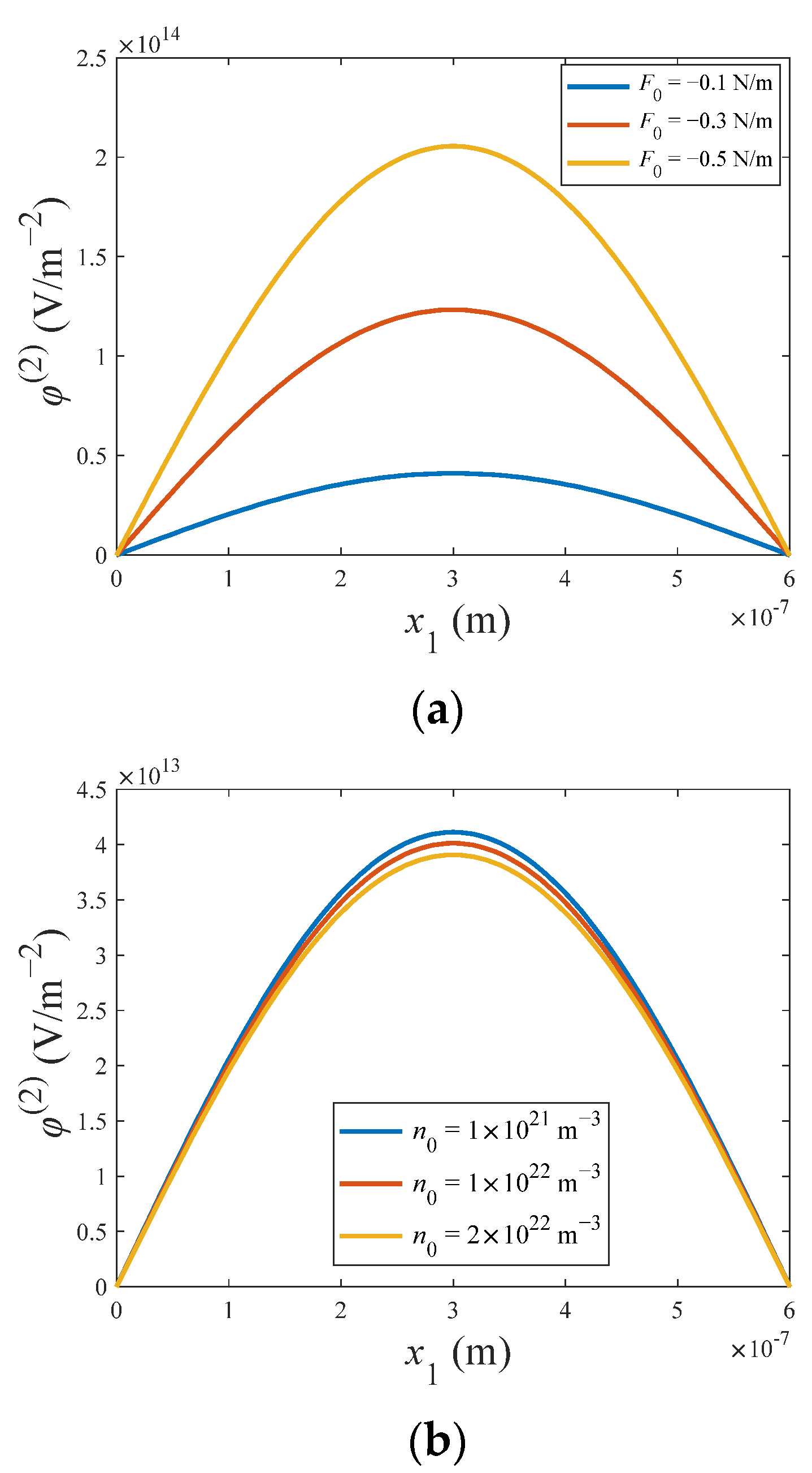
Figure 5 and Figure 6 depict the influence of load amplitude F0 and doping level n0 on the zeroth- and second-order electrostatic potential varying with x1, respectively. From Figure 5a and Figure 6a, it can be seen that the magnitude of electrostatic potential φ ( 0 ) and φ ( 2 ) increases with the increase of F0. Moreover, due to the screening effect of electrons on the electrostatic potential induced by piezoelectric effect, the magnitude of electrostatic potential will decrease when increasing the doping level (see Figure 5b and Figure 6b). In addition, electrostatic potential φ ( 0 ) and φ ( 2 ) will reach its maximum value when the semiconducting effect vanishes.

5. Conclusions

In this paper, the PVW for PSs is proposed. Different from classical approaches such as differential methods, this PVW is another method to establish structural theories, which will derive the field equations and boundary conditions simultaneously. Then, the field equations and corresponding boundary conditions are derived by directly applying the PVW and the Bernoulli–Euler beam theory with the aid of the second-order approximation of electrostatic potential. The correct 1-D constitutive relations are given by taking into account the relaxation procedure. Then, the 1-D PS nanowires model, which can be decoupled into extensional groups and bending groups, is obtained immediately.
As applications of the 1-D PS nanowires model, extension and bending deformation for ZnO nanowires are investigated. The mechanical displacement, electrostatic potential, and concentration of electrons for extension and bending deformation are analytically derived. From the numerical results, the distribution of electrostatic potential is anti-symmetric along the thickness direction for extension deformation, while bending deformation causes a symmetric distribution of electrostatic potential. Moreover, extension and bending deformation lead to a redistribution of electrons. The electrostatic potential can be tuned by adjusting the amplitude of the applied mechanical load. Finally, electrons redistribute themselves to screen the effective polarization and thus decrease the magnitude of the electrostatic potential.
The use of PVW can help to establish structural theories and provide an effective way of implementing numerical calculation methods.

Author Contributions

Conceptualization, Y.Q. and G.Z.; methodology, Y.Q., G.Z. and J.C.; writing—original draft preparation, J.C.; writing—review and editing, Y.Q., G.Z. and D.L. All authors have read and agreed to the published version of the manuscript.

Funding

This work reported here was funded by the National Natural Science Foundation of China (Grant No. 12002086 (G. Y. Zhang)), Fundamental Research Funds for the Central Universities (Grant No. 2242022R40040 (G. Y. Zhang)), and China Postdoctoral Science Foundation (Grant No. 2023M732863, (Y. L. Qu)).

Data Availability Statement

The authors attest that all data for this study are included in the paper.

Conflicts of Interest

The authors declare no conflict of interest.

References

  1. Auld, B.A. Acoustic Fields and Waves in Solids; John Wiley & Sons: New York, NY, USA, 1973. [Google Scholar]
  2. Hickernell, F.S. The piezoelectric semiconductor and acoustoelectronic device development in the sixties. IEEE Trans. Ultrason. Ferroelectr. Freq. Control 2005, 52, 737–745. [Google Scholar] [CrossRef] [PubMed]
  3. Wang, Z.L. Nanobelts, nanowires, and nanodiskettes of semiconducting oxides—From materials to nanodevices. Adv. Mater. 2003, 15, 432–436. [Google Scholar] [CrossRef]
  4. Lao, C.S.; Liu, J.; Gao, P.; Zhang, L.; Davidovic, D.; Tummala, R.; Wang, Z.L. ZnO nanobelt/nanowire Schottky diodes formed by dielectrophoresis alignment across Au electrodes. Nano Lett. 2006, 6, 263–266. [Google Scholar] [CrossRef]
  5. Kim, K.K.; Kim, H.S.; Hwang, D.K.; Lim, J.H.; Park, S.J. Realization of p-type ZnO thin films via phosphorus doping and thermal activation of the dopant. Appl. Phys. Lett. 2003, 83, 63–65. [Google Scholar] [CrossRef]
  6. Wang, Z.L. Piezotronics and Piezo-Phototronics; Springer: Berlin/Heidelberg, Germany, 2012. [Google Scholar]
  7. Wang, Z.L.; Song, J. Piezoelectric nanogenerators based on zinc oxide nanowire arrays. Science 2006, 312, 242–246. [Google Scholar] [CrossRef]
  8. Sharma, J.N.; Sharma, K.K.; Kumar, A. Surface waves in a piezoelectric–semiconductor composite structure. Int. J. Solids Struct. 2010, 47, 816–826. [Google Scholar] [CrossRef]
  9. Tian, R.; Liu, J.; Pan, E.; Wang, Y.; Soh, A.K. Some characteristics of elastic waves in a piezoelectric semiconductor plate. J. Appl. Phys. 2019, 126, 125701. [Google Scholar] [CrossRef]
  10. Cao, X.; Hu, S.; Liu, J.; Shi, J. Generalized Rayleigh surface waves in a piezoelectric semiconductor half space. Meccanica 2019, 54, 271–281. [Google Scholar] [CrossRef]
  11. Gokhale, V.J.; Rais-Zadeh, M. Phonon-electron interactions in piezoelectric semiconductor bulk acoustic wave resonators. Sci. Rep. 2014, 4, 1–10. [Google Scholar] [CrossRef]
  12. Sladek, J.; Sladek, V.; Pan, E.; Young, D.L. Dynamic anti-plane crack analysis in functional graded piezoelectric semiconductor crystals. CMES 2014, 99, 273–296. [Google Scholar]
  13. Fan, C.; Yan, Y.; Xu, G.; Zhao, M. Piezoelectric-conductor iterative method for analysis of cracks in piezoelectric semiconductors via the finite element method. Eng. Fract. Mech. 2016, 165, 183–196. [Google Scholar] [CrossRef]
  14. Qin, G.; Lu, C.; Zhang, X.; Zhao, M. Electric current dependent fracture in GaN piezoelectric semiconductor ceramics. Materials 2018, 11, 2000. [Google Scholar] [CrossRef] [PubMed]
  15. Zhang, C.L.; Luo, Y.X.; Cheng, R.R.; Wang, X.Y. Electromechanical fields in piezoelectric semiconductor nanofibers under an axial force. MRS Adv. 2017, 2, 3421. [Google Scholar] [CrossRef]
  16. Zhang, C.; Wang, X.; Chen, W.; Yang, J. An analysis of the extension of a ZnO piezoelectric semiconductor nanofiber under an axial force. Smart Mater. Struct. 2017, 26, 025030. [Google Scholar] [CrossRef]
  17. Jin, L.S.; Yan, X.H.; Wang, X.F.; Hu, W.J.; Zhang, Y.; Li, L.J. Dynamic model for piezotronic and piezo-phototronic devices under low and high frequency external compressive stresses. J. Appl. Phys. 2018, 123, 025709. [Google Scholar] [CrossRef]
  18. Qu, Y.L.; Jin, F.; Yang, J.S. Torsion of a piezoelectric semiconductor rod of cubic crystals with consideration of warping and in-plane shear of its rectangular cross section. Mech. Mater. 2022, 172, 104407. [Google Scholar] [CrossRef]
  19. Fang, K.; Qian, Z.; Yang, J. Piezopotential in a composite cantilever of piezoelectric dielectrics and nonpiezoelectric semiconductors produced by shear force through e15. Mater. Res. Express 2019, 6, 115917. [Google Scholar] [CrossRef]
  20. Ren, C.; Wang, K.F.; Wang, B.L. Adjusting the electromechanical coupling behaviors of piezoelectric semiconductor nanowires via strain gradient and flexoelectric effects. J. Appl. Phys. 2020, 128, 215701. [Google Scholar] [CrossRef]
  21. Yang, J.S. Analysis of Piezoelectric Semiconductor Structures; Springer: Cham, Switzerland, 2020. [Google Scholar]
  22. Qu, Y.L.; Jin, F.; Yang, J.S. Stress-induced electric potential barriers in thickness-stretch deformations of a piezoelectric semiconductor plate. Acta Mech. 2021, 232, 4533–4543. [Google Scholar] [CrossRef]
  23. Qu, Y.L.; Jin, F.; Yang, J.S. Buckling of a Reissner–Mindlin plate of piezoelectric semiconductors. Meccanica 2022, 57, 2797–2807. [Google Scholar] [CrossRef]
  24. Xu, C.; Wei, P.; Wei, Z.; Guo, X. Rayleigh wave in layered piezoelectric semiconductor with consideration of PN junction effects. Math. Mech. Solids 2022, 28, 1817–1833. [Google Scholar] [CrossRef]
  25. Xu, C.; Wei, P.; Wei, Z.; Guo, X. Effects of Schottky junction on surface waves in a piezoelectric semiconducting film over a metal substrate. Math. Mech. Solids 2023. Online. [Google Scholar] [CrossRef]
  26. Qu, Y.L.; Pan, E.N.; Zhu, F.; Jin, F.; Roy, A.K. Modeling thermoelectric effects in piezoelectric semiconductors: New fully coupled mechanisms for mechanically manipulated heat flux and refrigeration. Int. J. Eng. Sci. 2023, 182, 103775. [Google Scholar] [CrossRef]
  27. Zhou, J.; Fei, P.; Gao, Y.; Gu, Y.; Liu, J.; Bao, G.; Wang, Z.L. Mechanical-electrical triggers and sensors using piezoelectric micowires/nanowires. Nano Lett. 2008, 8, 2725–2730. [Google Scholar] [CrossRef]
  28. Liang, C.; Zhang, C.; Chen, W.; Yang, J. Static buckling of piezoelectric semiconductor fibers. Mater. Res. Express 2020, 6, 125919. [Google Scholar] [CrossRef]
  29. Zhang, Z.; Liang, C.; Wang, Y.; Xu, R.; Gao, C.; Zhang, C. Static bending and vibration analysis of piezoelectric semiconductor beams considering surface effects. J. Vib. Eng. Technol. 2021, 9, 1789–1800. [Google Scholar] [CrossRef]
  30. Zhang, Z.; Liang, C.; Kong, D.; Xiao, Z.; Zhang, C.; Chen, W. Dynamic buckling and free bending vibration of axially compressed piezoelectric semiconductor rod with surface effect. Int. J. Appl. Mech. 2023, 238, 107823. [Google Scholar] [CrossRef]
  31. Luo, Y.; Zhang, C.; Chen, W.; Yang, J. Piezopotential in a bended composite fiber made of a semiconductive core and of two piezoelectric layers with opposite polarities. Nano Energy 2018, 54, 341–348. [Google Scholar] [CrossRef]
  32. Maugin, G.A. The method of virtual power in continuum mechanics: Application to coupled fields. Acta Mech. 1980, 35, 1–70. [Google Scholar] [CrossRef]
  33. Daher, N.; Maugin, G.A. Virtual power and thermodynamics for electromagnetic continua with interfaces. J. Math. Phys. 1986, 27, 3022–3035. [Google Scholar] [CrossRef]
  34. Maugin, G.A. The principle of virtual power: From eliminating metaphysical forces to providing an efficient modelling tool: In memory of Paul Germain (1920–2009). Continuum Mech. Therm. 2013, 25, 127–146. [Google Scholar] [CrossRef]
  35. Falsone, G.; La Valle, G. A homogenized theory for functionally graded Euler–Bernoulli and Timoshenko beams. Acta Mech. 2019, 230, 3511–3523. [Google Scholar] [CrossRef]
  36. Ascione, A.; Gherlone, M.; Orifici, A.C. Nonlinear static analysis of composite beams with piezoelectric actuator patches using the Refined Zigzag Theory. Compos. Struct. 2022, 282, 115018. [Google Scholar] [CrossRef]
  37. Germain, P. The method of virtual power in the mechanics of continuous media, I: Second-gradient theory. Math. Mech. Complex Sy. 2020, 8, 153–190. [Google Scholar] [CrossRef]
  38. Qu, Y.L.; Zhang, G.Y.; Fan, Y.M.; Jin, F. A non-classical theory of elastic dielectrics incorporating couple stress and quadrupole effects: Part I – reconsideration of curvature-based flexoelectricity theory. Math. Mech. Solids 2021, 26, 1647–1659. [Google Scholar] [CrossRef]
  39. Yang, J.S. The Mechanics of Piezoelectric Structures; World Scientific: Singapore, 2006. [Google Scholar]
  40. Gao, X.-L.; Mall, S. Variational solution for a cracked mosaic model of woven fabric composites. Int. J. Solids Struct. 2001, 38, 855–874. [Google Scholar] [CrossRef]
  41. Qu, Y.L.; Jin, F.; Yang, J.S. Flexoelectric effects in second-order extension of rods. Mech. Res. Commun. 2021, 111, 103625. [Google Scholar] [CrossRef]
  42. Zhang, G.Y.; Guo, Z.W.; Qu, Y.L.; Gao, X.L.; Jin, F. A new model for thermal buckling of an anisotropic elastic composite beam incorporating piezoelectric, flexoelectric and semiconducting effects. Acta Mech. 2022, 233, 1719–1738. [Google Scholar] [CrossRef]
  43. Qu, Y.L.; Zhang, G.Y.; Gao, X.L.; Jin, F. A new model for thermally induced redistributions of free carriers in centrosymmetric flexoelectric semiconductor beams. Mech. Mater. 2022, 171, 104328. [Google Scholar] [CrossRef]
  44. Sze, S.M.; Ng, K.K. Physics of Semiconductor Devices; John Wiley & Sons: Hoboken, NJ, USA, 2007. [Google Scholar]
  45. Wang, G.; Liu, J.; Liu, X.; Feng, W.; Yang, J. Extensional vibration characteristics and screening of polarization charges in a ZnO piezoelectric semiconductor nanofiber. J. Appl. Phys. 2018, 124, 094502. [Google Scholar] [CrossRef]
  46. Zhang, G.Y.; Qu, Y.L.; Guo, Z.W.; Jin, F. Magnetically induced electric potential in first-order composite beams incorporating couple stress and its flexoelectric effects. Acta Mech. Sin. 2021, 37, 1509–1519. [Google Scholar] [CrossRef]
Figure 1. The coordinate system of PS nanowires.
Crystals 13 01368 g001
Figure 2. The (a) electrostatic potential, and (b) electron concentration of the ZnO nanowires subjected to an axial load f 1 ( 0 ) (with T0 = 0.1 N/m and n0 = 1 × 10²¹ m−3).
Crystals 13 01368 g002
Figure 3. Variations of the first-order electrostatic potential φ ( 1 ) for (a) different load amplitude T0 (with n0 = 1 × 10²¹ m−3) and (b) different doping level (with T0 = 0.1 N/m).
Crystals 13 01368 g003aCrystals 13 01368 g003b
Figure 4. The (a) electrostatic potential and (b) electron concentration of the ZnO nanowires subjected to a transverse load f 3 ( 0 ) (with F0 = −0.1 N/m and n0 = 1 × 10²¹ m−3).
Crystals 13 01368 g004
Figure 5. Variations of the zeroth-order electrostatic potential φ ( 0 ) for (a) different load amplitude F0 (with n0 = 1 × 10²¹ m−3) and (b) different doping level (with F0 = −0.1 N/m).
Crystals 13 01368 g005
Figure 6. Variations of the second-order electrostatic potential φ ( 2 ) for (a) different load amplitude F0 (with n0 = 1 × 10²¹ m−3) and (b) different doping level (with F0 = −0.1 N/m).
Crystals 13 01368 g006
Disclaimer/Publisher’s Note: The statements, opinions and data contained in all publications are solely those of the individual author(s) and contributor(s) and not of MDPI and/or the editor(s). MDPI and/or the editor(s) disclaim responsibility for any injury to people or property resulting from any ideas, methods, instructions or products referred to in the content.