

Transistor-Based Synaptic Devices for Neuromorphic Computing


Abstract
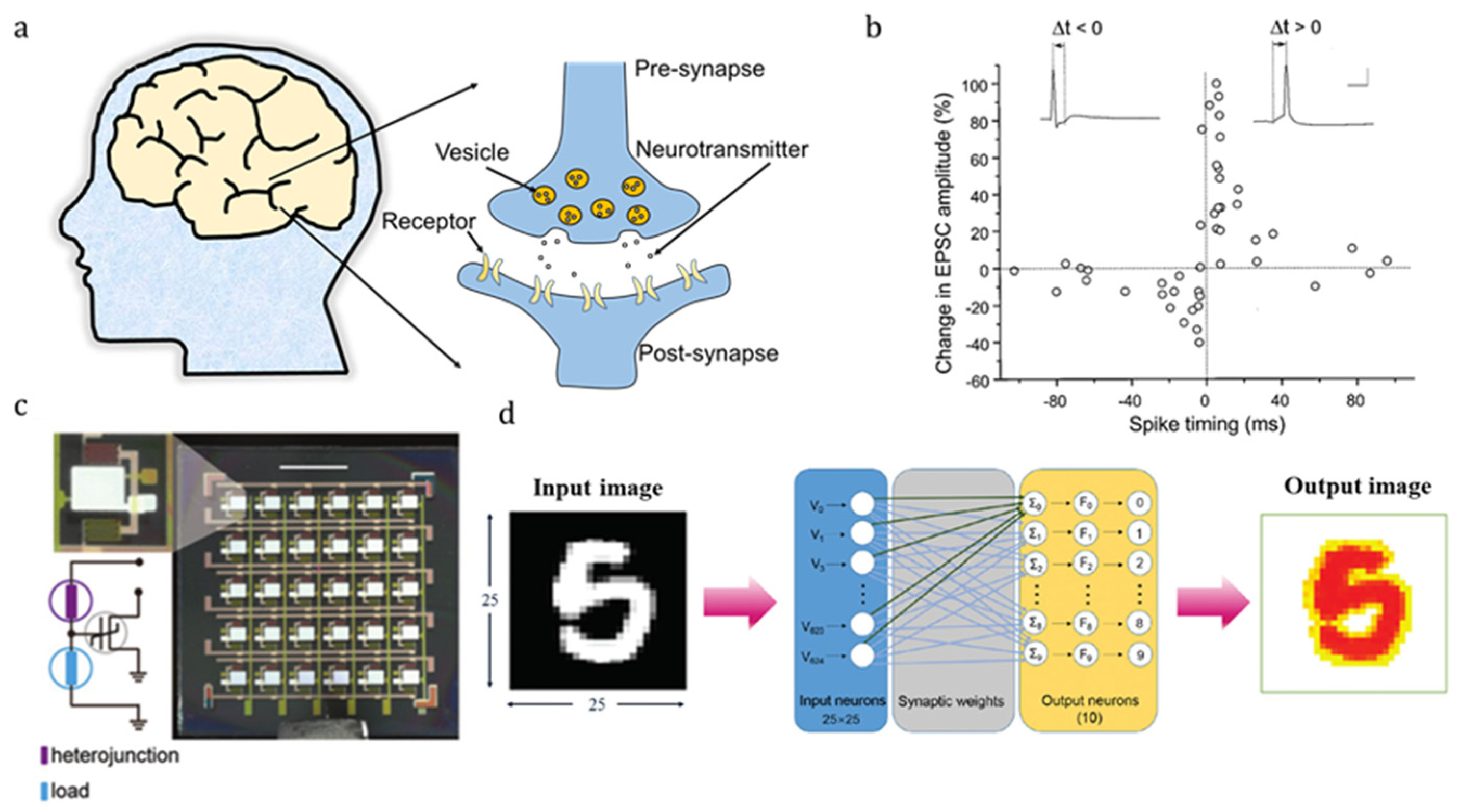
1. Introduction
2. Different Working Mechanisms of Synaptic Transistor Devices
2.1. Capture and Release of Carriers

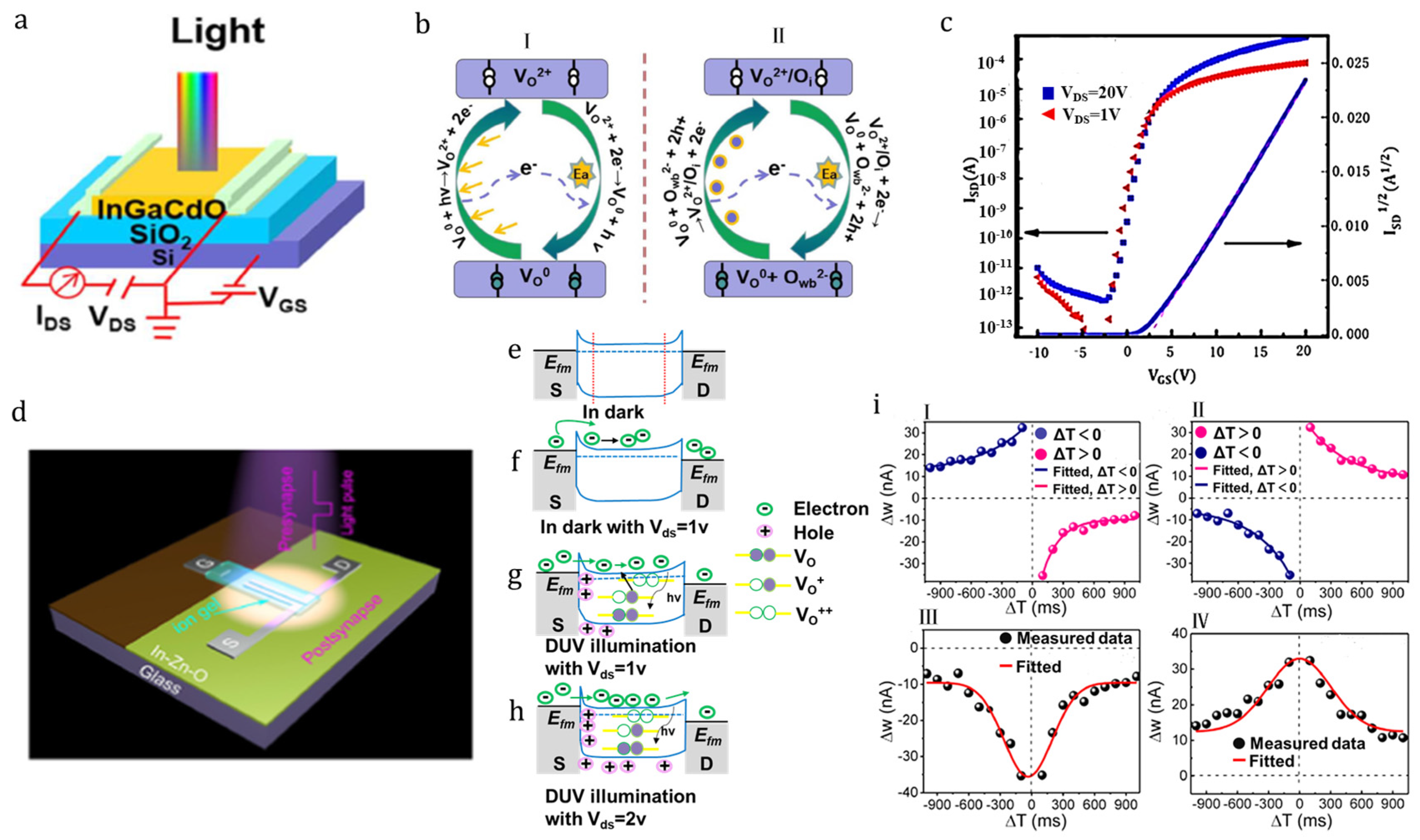
2.2. Ionization and Neutralization of Oxygen Vacancies
2.3. Ion-Gated Synaptic Transistors
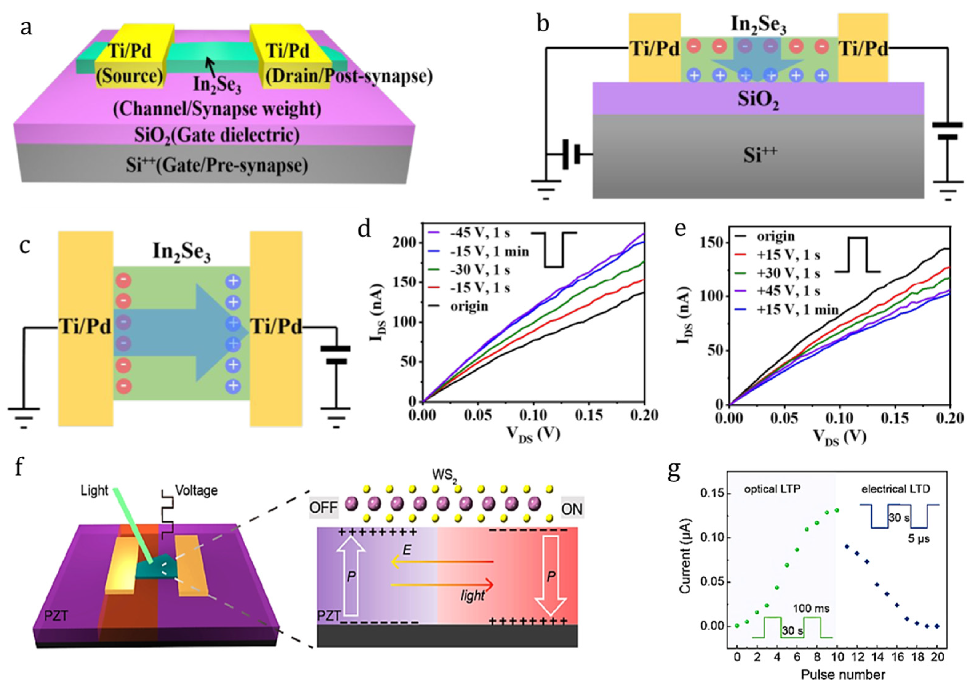
2.4. Ferroelectric Polarization
3. Perspectives
4. Conclusions
Author Contributions
Funding
Data Availability Statement
Conflicts of Interest
References
- Bi, G.; Poo, M. Synaptic modifications in cultured hippocampal neurons: Dependence on spike timing, synaptic strength, and postsynaptic cell type. J. Neurosci. 1998, 18, 10464–10472. [Google Scholar] [CrossRef] [PubMed]
- Jin, C.; Liu, W.; Huang, Y.; Xu, Y.; Nie, Y.; Zhang, G.; He, P.; Sun, J.; Yang, J. Printable ion-gel-gated In2O3 synaptic transistor array for neuro-inspired memory. Appl. Phys. Lett. 2022, 120, 233701. [Google Scholar] [CrossRef]
- Lan, S.; Zhong, J.; Chen, J.; He, W.; He, L.; Yu, R.; Chen, G.; Chen, H. An optoelectronic synaptic transistor with efficient dual modulation by light illumination. J. Mater. Chem. C 2021, 9, 3412–3420. [Google Scholar] [CrossRef]
- Waldrop, M.M. The chips are down for Moore’s law. Nat. News 2016, 530, 7589. [Google Scholar] [CrossRef]
- Zhu, S.; Yu, T.; Xu, T.; Chen, H.; Dustdar, S.; Gigan, S.; Pan, Y. Intelligent computing: The latest advances, challenges, and future. Intell. Comput. 2023, 2, 0006. [Google Scholar] [CrossRef]
- Markram, H. The blue brain project. Nat. Rev. Neurosci. 2006, 7, 153–160. [Google Scholar] [CrossRef] [PubMed]
- Zhu, J.; Zhang, T.; Yang, Y.; Huang, R. A comprehensive review on emerging artificial neuromorphic devices. Appl. Phys. Rev. 2020, 7, 011312. [Google Scholar] [CrossRef]
- Zidan, M.A.; Strachan, J.P.; Lu, W.D. The future of electronics based on memristive systems. Nat. Electron. 2018, 1, 22–29. [Google Scholar] [CrossRef]
- Cohen-Cory, S. The Developing Synapse: Construction and Modulation of Synaptic Structures and Circuits. Science 2002, 298, 770–776. [Google Scholar] [CrossRef]
- Kuzum, D.; Yu, S.; Wong, H.P. Synaptic electronics: Materials, devices and applications. Nanotechnology 2013, 24, 382001. [Google Scholar] [CrossRef]
- Abbott, L.F.; Regehr, W.G. Synaptic computation. Nature 2004, 431, 796–803. [Google Scholar] [CrossRef] [PubMed]
- Zucker, R.S.; Regehr, W.G. Short-term synaptic plasticity. Annu. Rev. Physiol. 2002, 64, 355–405. [Google Scholar] [CrossRef] [PubMed]
- Atluri, P.P.; Regehr, W.G. Determinants of the Time Course of Facilitation at the Granule Cell to Purkinje Cell Synapse. J. Neurosci. 1996, 16, 5661–5671. [Google Scholar] [CrossRef] [PubMed]
- Rotman, Z.; Deng, P.-Y.; Klyachko, V.A. Short-Term Plasticity Optimizes Synaptic Information Transmission. J. Neurosci. 2011, 31, 14800–14809. [Google Scholar] [CrossRef] [PubMed]
- Fioravante, D.; Regehr, W.G. Short-term forms of presynaptic plasticity. Curr. Opin. Neurobiol. 2011, 21, 269–274. [Google Scholar] [CrossRef] [PubMed]
- Royer, S.; Paré, D. Conservation of total synaptic weight through balanced synaptic depression and potentiation. Nature 2003, 422, 518–522. [Google Scholar] [CrossRef] [PubMed]
- Harris, J.J.; Jolivet, R.; Attwell, D. Synaptic Energy Use and Supply. Neuron 2012, 75, 762–777. [Google Scholar] [CrossRef] [PubMed]
- Tang, J.; Yuan, F.; Shen, X.; Wang, Z.; Rao, M.; He, Y.; Wu, H. Bridging biological and artificial neural networks with emerging neuromorphic devices: Fundamentals, progress, and challenges. Adv. Mater. 2019, 31, 1902761. [Google Scholar] [CrossRef]
- Lee, H.E.; Park, J.H.; Kim, T.J.; Im, D.; Shin, J.H.; Kim, D.H.; Mohammad, B.; Kang, I.-S.; Lee, K.J. Novel Electronics for Flexible and Neuromorphic Computing. Adv. Funct. Mater. 2018, 28, 1801690. [Google Scholar] [CrossRef]
- Mao, J.; Zhou, L.; Zhu, X.; Zhou, Y.; Han, S. Photonic Memristor for Future Computing: A Perspective. Adv. Opt. Mater. 2019, 7, 1900766. [Google Scholar] [CrossRef]
- Zhang, J.; Dai, S.; Zhao, Y.; Zhang, J.; Huang, J. Recent Progress in Photonic Synapses for Neuromorphic Systems. Adv. Intell. Syst. 2020, 2, 1900136. [Google Scholar] [CrossRef]
- Jin, C.; Liu, W.; Xu, Y.; Huang, Y.; Nie, Y.; Shi, X.; Yang, J. Artificial vision adaption mimicked by an optoelectrical In2O3 transistor array. Nano Lett. 2022, 22, 3372–3379. [Google Scholar] [CrossRef] [PubMed]
- Sun, J.; Oh, S.; Choi, Y.; Seo, S.; Oh, M.J.; Lee, M.; Lee, W.B.; Yoo, P.J.; Cho, J.H.; Park, J. Optoelectronic Synapse Based on IGZO-Alkylated Graphene Oxide Hybrid Structure. Adv. Funct. Mater. 2018, 28, 1804397. [Google Scholar] [CrossRef]
- Sun, K.; Chen, J.; Yan, X. The Future of Memristors: Materials Engineering and Neural Networks. Adv. Funct. Mater. 2021, 31, 2006773. [Google Scholar] [CrossRef]
- Zhuo, F.; Wu, J.; Li, B.; Li, M.; Tan, C.L.; Luo, Z.; Sun, H.; Xu, Y.; Yu, Z. Modifying the Power and Performance of 2-Dimensional MoS 2 Field Effect Transistors. Research 2023, 6, 0057. [Google Scholar] [CrossRef]
- Yan, B.; Yang, Y.; Huang, R. Memristive dynamics enabled neuromorphic computing systems. Sci. China Inf. Sci. 2023, 66, 200401. [Google Scholar] [CrossRef]
- Cheng, Y.; Lin, Y.; Zeng, T.; Shan, X.; Wang, Z.; Zhao, X.; Ielmini, D.; Xu, H.; Liu, Y. Pavlovian conditioning achieved via one-transistor/one-resistor memristive synapse. Appl. Phys. Lett. 2022, 120, 133503. [Google Scholar] [CrossRef]
- Fu, S.; Park, J.H.; Gao, H.; Zhang, T.; Ji, X.; Fu, T.; Yao, J. Two-terminal MoS2 memristor and the homogeneous integration with a MoS2 transistor for neural networks. Nano Lett. 2023, 23, 5869–5876. [Google Scholar] [CrossRef]
- Dai, S.; Zhao, Y.; Wang, Y.; Zhang, J.; Fang, L.; Jin, S.; Shao, Y.; Huang, J. Recent Advances in Transistor-Based Artificial Synapses. Adv. Funct. Mater. 2019, 29, 1903700. [Google Scholar] [CrossRef]
- Zhong, H.; Sun, Q.-C.; Li, G.; Du, J.-Y.; Huang, H.-Y.; Guo, E.-J.; He, M.; Wang, C.; Yang, G.-Z.; Ge, C.; et al. High-performance synaptic transistors for neuromorphic computing. Chin. Phys. B 2020, 29, 040703. [Google Scholar] [CrossRef]
- Xie, C.; You, P.; Liu, Z.; Li, L.; Yan, F. Ultrasensitive broadband phototransistors based on perovskite/organic-semiconductor vertical heterojunctions. Light. Sci. Appl. 2017, 6, e17023. [Google Scholar] [CrossRef] [PubMed]
- Monalisha, P.; Kumar, A.P.S.; Wang, X.R.; Piramanayagam, S.N. Emulation of Synaptic Plasticity on a Cobalt-Based Synaptic Transistor for Neuromorphic Computing. ACS Appl. Mater. Interfaces 2022, 14, 11864–11872. [Google Scholar] [CrossRef] [PubMed]
- Ding, Y.-X.; Huang, K.-W.; Chen, J.-W.; Hsu, H.-H.; Ying, L.-Y.; Zhang, B.-P.; Zheng, Z.-W. Oxide-based synaptic transistors gated by solid biopolymer electrolytes. J. Mater. Sci. 2023, 58, 11740–11747. [Google Scholar] [CrossRef]
- Zhang, X.; Li, B.; Wang, H.; Ding, Q.; Gao, S. Study of Electronic Synaptic Characteristics in PVA Organic Field-Effect Transistors. J. Electron. Mater. 2023, 52, 5307–5314. [Google Scholar] [CrossRef]
- Cui, J.; An, F.; Qian, J.; Wu, Y.; Sloan, L.L.; Pidaparthy, S.; Zuo, J.-M.; Cao, Q. CMOS-compatible electrochemical synaptic transistor arrays for deep learning accelerators. Nat. Electron. 2023, 6, 292–300. [Google Scholar] [CrossRef]
- Li, X.; Bi, R.; Ou, X.; Han, S.; Sheng, Y.; Chen, G.; Xie, Z.; Liu, C.; Yue, W.; Wang, Y.; et al. 3D-Printed Intrinsically Stretchable Organic Electrochemical Synaptic Transistor Array. ACS Appl. Mater. Interfaces 2023, 15, 41656–41665. [Google Scholar] [CrossRef] [PubMed]
- Mohanty, H.N.; Tsuruoka, T.; Mohanty, J.R.; Terabe, K. Proton-Gated Synaptic Transistors, Based on an Electron-Beam Patterned Nafion Electrolyte. ACS Appl. Mater. Interfaces 2023, 15, 19279–19289. [Google Scholar] [CrossRef]
- Zhang, J.; Liu, D.; Ou, Q.; Lu, Y.; Huang, J. Covalent Coupling of Porphyrins with Monolayer Graphene for Low-Voltage Synaptic Transistors. ACS Appl. Mater. Interfaces 2022, 14, 11699–11707. [Google Scholar] [CrossRef]
- Xia, F.; Xia, T.; Xiang, L.; Ding, S.; Li, S.; Yin, Y.; Xi, M.; Jin, C.; Liang, X.; Hu, Y. Carbon Nanotube-Based Flexible Ferroelectric Synaptic Transistors for Neuromorphic Computing. ACS Appl. Mater. Interfaces 2022, 14, 30124–30132. [Google Scholar] [CrossRef]
- Nandan, K.; Naseer, A.; Chauhan, Y.S. Field-Effect Transistors Based on Two-dimensional Materials (Invited). Trans. Indian Natl. Acad. Eng. 2022, 8, 1–14. [Google Scholar] [CrossRef]
- Zhang, C.; He, T.; Zhao, J.; Liu, G.; Wang, Z.; Zhang, C. Tribo-thermoelectric and tribovoltaic coupling effect at metal-semiconductor interface. Mater. Today Phys. 2020, 16, 100295. [Google Scholar] [CrossRef]
- Yin, L.; Huang, W.; Xiao, R.; Peng, W.; Zhu, Y.; Zhang, Y.; Pi, X.; Yang, D. Optically Stimulated Synaptic Devices Based on the Hybrid Structure of Silicon Nanomembrane and Perovskite. Nano Lett. 2020, 20, 3378–3387. [Google Scholar] [CrossRef] [PubMed]
- Liu, Z.; Dai, S.; Wang, Y.; Yang, B.; Hao, D.; Liu, D.; Zhao, Y.; Fang, L.; Ou, Q.; Jin, S.; et al. Photoresponsive Transistors Based on Lead-Free Perovskite and Carbon Nanotubes. Adv. Funct. Mater. 2020, 30, 1906335. [Google Scholar] [CrossRef]
- Li, H.K.; Chen, T.P.; Liu, P.; Hu, S.G.; Liu, Y.; Zhang, Q.; Lee, P.S. A light-stimulated synaptic transistor with synaptic plasticity and memory functions based on InGaZnOx–Al2O3 thin film structure. J. Appl. Phys. 2016, 119, 244505. [Google Scholar] [CrossRef]
- Hao, D.; Zhang, J.; Dai, S.; Zhang, J.; Huang, J. Perovskite/Organic Semiconductor-Based Photonic Synaptic Transistor for Artificial Visual System. ACS Appl. Mater. Interfaces 2020, 12, 39487–39495. [Google Scholar] [CrossRef]
- Liu, J.; Yang, Z.; Gong, Z.; Shen, Z.; Ye, Y.; Yang, B.; Qiu, Y.; Ye, B.; Xu, L.; Guo, T.; et al. Weak Light-Stimulated Synaptic Hybrid Phototransistors Based on Islandlike Perovskite Films Prepared by Spin Coating. ACS Appl. Mater. Interfaces 2021, 13, 13362–13371. [Google Scholar] [CrossRef]
- Wang, K.; Dai, S.; Zhao, Y.; Wang, Y.; Liu, C.; Huang, J. Light-Stimulated Synaptic Transistors Fabricated by a Facile Solution Process Based on Inorganic Perovskite Quantum Dots and Organic Semiconductors. Small 2019, 15, e1900010. [Google Scholar] [CrossRef]
- Indiveri, G.; Chicca, E.; Douglas, R.J. Artificial Cognitive Systems: From VLSI Networks of Spiking Neurons to Neuromorphic Cognition. Cogn. Comput. 2009, 1, 119–127. [Google Scholar] [CrossRef]
- Van De Burgt, Y.Y.; Lubberman, E.; Fuller, E.J.; Keene, S.; Faria, G.C.; Agarwal, S.; Marinella, M.J.; Talin, A.; Salleo, A. A non-volatile organic electrochemical device as a low-voltage artificial synapse for neuromorphic computing. Nat. Mater. 2017, 16, 414–418. [Google Scholar] [CrossRef]
- Chetyrkina, M.R.; Kameneva, L.; Mishchenko, D.V.; Klimanova, E.N.; Sashenkova, T.E.; Allayarova, U.Y.; Kostyuk, S.V.; Frolova, L.A.; Aldoshin, S.M.; Troshin, P.A. Lead, tin, bismuth or organics: Assessment of potential environmental and human health hazards originating from mature perovskite PV technology. Sol. Energy Mater. Sol. Cells 2023, 252, 112177. [Google Scholar] [CrossRef]
- Yue, Z.; Guo, H.; Cheng, Y. Toxicity of Perovskite Solar Cells. Energies 2023, 16, 4007. [Google Scholar] [CrossRef]
- Yin, Y.; Yang, L.; Zhang, X.; Zhang, J. Pernicious effects and management of lead leakage from perovskite solar cells. J. Mater. Chem. A 2023, 11, 25825–25848. [Google Scholar] [CrossRef]
- Chen, C.; Cheng, S.; Cheng, L.; Wang, Z.; Liao, L. Toxicity, Leakage, and Recycling of Lead in Perovskite Photovoltaics. Adv. Energy Mater. 2023, 13, 2204144. [Google Scholar] [CrossRef]
- Chai, W.; Li, L.; Zhu, W.; Chen, D.; Zhou, L.; Xi, H.; Zhang, J.; Zhang, C.; Hao, Y. Graded Heterojunction Improves Wide-Bandgap Perovskite for Highly Efficient 4-Terminal Perovskite/Silicon Tandem Solar Cells. Research 2023, 6, 0196. [Google Scholar] [CrossRef] [PubMed]
- Zhou, Z.; Li, Q.; Chen, M.; Zheng, X.; Wu, X.; Lu, X.; Tao, S.; Zhao, N. High-Mobility and Bias-Stable Field-Effect Transistors Based on Lead-Free Formamidinium Tin Iodide Perovskites. ACS Energy Lett. 2023, 8, 4496–4505. [Google Scholar] [CrossRef] [PubMed]
- Zhang, F.; Shao, M.; Wang, C.; Wen, W.; Shi, W.; Qin, M.; Liu, Y. Photoinduced nonvolatile memory transistor based on lead-free perovskite incorporating fused Π-conjugated organic ligands. Adv. Mater. 2023, 2307326. [Google Scholar] [CrossRef] [PubMed]
- Chao, I.; Yang, Y.; Yu, M.; Chen, C.; Liao, C.; Lin, B.; Ni, I.; Chen, W.; Ho-Baillie, A.W.Y.; Chueh, C. Performance Enhancement of Lead-Free 2D Tin Halide Perovskite Transistors by Surface Passivation and Its Impact on Non-Volatile Photomemory Characteristics. Small 2023, 19, e2207734. [Google Scholar] [CrossRef]
- Geng, X.; Chen, Y.A.; Li, Y.Y.; Ren, J.; Dun, G.H.; Qin, K.; Ren, T.L. Lead-free halide perovskites for direct X-ray detectors. Adv. Sci. 2023, 10, 2300256. [Google Scholar] [CrossRef]
- Wei, Z.; Ding, L.; Sun, N.; Dang, L.-Y.; Sun, H.-R.; Han, J.-C.; Zhu, J.-Q.; Wang, G.-G. Lead-free CsBi3I10 perovskite based photo-enhanced triboelectric nanogenerator. Nano Energy 2023, 108, 108209. [Google Scholar] [CrossRef]
- Li, G.; Rivarola, F.W.R.; Davis, N.J.L.K.; Bai, S.; Jellicoe, T.C.; de la Peña, F.; Hou, S.; Ducati, C.; Gao, F.; Friend, R.H.; et al. Highly Efficient Perovskite Nanocrystal Light-Emitting Diodes Enabled by a Universal Crosslinking Method. Adv. Mater. 2016, 28, 3528–3534. [Google Scholar] [CrossRef]
- Takimiya, K.; Osaka, I.; Mori, T.; Nakano, M. Organic semiconductors based on [1] benzothieno [3, 2-b][1] benzothiophene substructure. Acc. Chem. Res. 2014, 47, 1493–1502. [Google Scholar] [CrossRef]
- Lin, Z.; Lei, J.; Wang, P.; Xu, L.; Zhang, X.; Kang, Y.; Chen, M.; Wei, G. Effects of Bromine Substitution and Vacancy Defects on the Structural and Electronic Properties of Black Orthorhombic CsPbI3 Perovskite. Phys. Status Solidi (RRL) Rapid Res. Lett. 2021, 15, 2100277. [Google Scholar] [CrossRef]
- Maier, J. Defect chemistry: Composition, transport, and reactions in the solid state; part II: Kinetics. Angew. Chem. Int. Ed. Engl. 1993, 32, 528–542. [Google Scholar] [CrossRef]
- Chen, J.; Chang, X.; Guo, J.; Gao, Q.; Zhang, X.; Liu, C.; Chen, J. Organic passivation of deep defects in Cu(In,Ga)Se2 film for geometry-simplified compound solar cells. Research 2023, 6, 0084. [Google Scholar] [CrossRef] [PubMed]
- Qin, X.; Lu, W.; Wang, X.; Qin, Z.; Chen, H.; Lu, G.; Lu, G.; Bu, L. Surface-modified polydimethylsiloxane with soft-plasma as dielectric layer for flexible artificial synaptic transistors. Appl. Surf. Sci. 2023, 627, 157325. [Google Scholar] [CrossRef]
- Wang, J.; Yang, B.; Dai, S.; Guo, P.; Gao, Y.; Li, L.; Huang, J. Weak light-stimulated synaptic transistors based on MoS2/organic semiconductor heterojunction for neuromorphic computing. Adv. Mater. Technol. 2023, 8, 2300449. [Google Scholar] [CrossRef]
- Liu, X.; Huang, W.; Kai, C.; Yin, L.; Wang, Y.; Liu, X.; Yang, D. Photogated synaptic transistors based on the heterostructure of 4H-SiC and organic semiconductors for neuromorphic ultraviolet vision. ACS Appl. Electron. Mater. 2023, 5, 367–374. [Google Scholar] [CrossRef]
- Zhou, R.; Zhang, W.; Cong, H.; Chang, Y.; Wang, F.; Liu, X. Metal oxide semiconductor nanowires enabled air-stable ultraviolet-driven synaptic transistors for artificial vision. Mater. Sci. Semicond. Process. 2023, 158, 107344. [Google Scholar] [CrossRef]
- Kim, H.; Park, J.; Kwon, M.-W.; Lee, J.-H.; Park, B.-G. Silicon-Based Floating-Body Synaptic Transistor with Frequency-Dependent Short- and Long-Term Memories. IEEE Electron Device Lett. 2016, 37, 249–252. [Google Scholar] [CrossRef]
- Seo, Y.-T.; Kwon, D.; Noh, Y.; Lee, S.; Park, M.-K.; Woo, S.Y.; Park, B.-G.; Lee, J.-H. 3-D AND-Type Flash Memory Architecture with High-κ Gate Dielectric for High-Density Synaptic Devices. IEEE Trans. Electron Devices 2021, 68, 3801–3806. [Google Scholar] [CrossRef]
- Kumar, M.; Abbas, S.; Kim, J. All-Oxide-Based Highly Transparent Photonic Synapse for Neuromorphic Computing. ACS Appl. Mater. Interfaces 2018, 10, 34370–34376. [Google Scholar] [CrossRef] [PubMed]
- Guan, X.; Wang, Z.; Hota, M.K.; Alshareef, H.N.; Wu, T. P-type SnO thin film phototransistor with perovskite-mediated photogating. Adv. Electron. Mater. 2019, 5, 1800538. [Google Scholar] [CrossRef]
- Duan, H.; Javaid, K.; Liang, L.; Huang, L.; Yu, J.; Zhang, H.; Gao, J.; Zhuge, F.; Chang, T.-C.; Cao, H. Broadband Optoelectronic Synaptic Thin-Film Transistors Based on Oxide Semiconductors. Phys. Status Solidi (RRL) Rapid Res. Lett. 2020, 14, 1900630. [Google Scholar] [CrossRef]
- Wang, J.; Chen, Y.; Kong, L.-A.; Fu, Y.; Gao, Y.; Sun, J. Deep-ultraviolet-triggered neuromorphic functions in In-Zn-O phototransistors. Appl. Phys. Lett. 2018, 113, 151101. [Google Scholar] [CrossRef]
- Jeon, S.; Ahn, S.-E.; Song, I.; Kim, C.J.; Chung, U.-I.; Lee, E.; Yoo, I.; Nathan, A.; Lee, S.; Ghaffarzadeh, K.; et al. Gated three-terminal device architecture to eliminate persistent photoconductivity in oxide semiconductor photosensor arrays. Nat. Mater. 2012, 11, 301–305. [Google Scholar] [CrossRef] [PubMed]
- Ahn, S.; Song, I.; Jeon, S.; Jeon, Y.W.; Kim, Y.; Kim, C.; Ryu, B.; Lee, J.; Nathan, A.; Lee, S.; et al. Metal Oxide Thin Film Phototransistor for Remote Touch Interactive Displays. Adv. Mater. 2012, 24, 2631–2636. [Google Scholar] [CrossRef] [PubMed]
- Lee, M.; Lee, W.; Choi, S.; Jo, J.; Kim, J.; Park, S.K.; Kim, Y. Brain-Inspired Photonic Neuromorphic Devices using Photodynamic Amorphous Oxide Semiconductors and their Persistent Photoconductivity. Adv. Mater. 2017, 29, 1700951. [Google Scholar] [CrossRef] [PubMed]
- Zhang, C.; Li, S.; He, Y.; Chen, C.; Jiang, S.; Yang, X.; Wang, X.; Pan, L.; Wan, Q. Oxide Synaptic Transistors Coupled with Triboelectric Nanogenerators for Bio-Inspired Tactile Sensing Application. IEEE Electron Device Lett. 2020, 41, 617–620. [Google Scholar] [CrossRef]
- Peng, C.; Jiang, W.; Li, Y.; Li, X.; Zhang, J. Photoelectric IGZO Electric-Double-Layer Transparent Artificial Synapses for Emotional State Simulation. ACS Appl. Electron. Mater. 2019, 1, 2406–2414. [Google Scholar] [CrossRef]
- Yu, J.; Liang, L.; Hu, L.; Duan, H.; Wu, W.; Zhang, H.; Gao, J.; Zhuge, F.; Chang, T.; Cao, H. Optoelectronic neuromorphic thin-film transistors capable of selective attention and with ultra-low power dissipation. Nano Energy 2019, 62, 772–780. [Google Scholar] [CrossRef]
- Kim, H.; Hwang, S.; Park, J.; Park, B.-G. Silicon synaptic transistor for hardware-based spiking neural network and neuromorphic system. Nanotechnology 2017, 28, 405202. [Google Scholar] [CrossRef] [PubMed]
- Covi, E.; Brivio, S.; Serb, A.; Prodromakis, T.; Fanciulli, M.; Spiga, S. Analog Memristive Synapse in Spiking Networks Implementing Unsupervised Learning. Front. Neurosci. 2016, 10, 482. [Google Scholar] [CrossRef] [PubMed]
- Leighton, C. Electrolyte-based ionic control of functional oxides. Nat. Mater. 2018, 18, 13–18. [Google Scholar] [CrossRef] [PubMed]
- Dai, S.; Chu, Y.; Liu, D.; Cao, F.; Wu, X.; Zhou, J.; Zhou, B.; Chen, Y.; Huang, J. Intrinsically ionic conductive cellulose nanopapers applied as all solid dielectrics for low voltage organic transistors. Nat. Commun. 2018, 9, 2737. [Google Scholar] [CrossRef] [PubMed]
- Fujimoto, T.; Awaga, K. Electric-double-layer field-effect transistors with ionic liquids. Phys. Chem. Chem. Phys. 2013, 15, 8983–9006. [Google Scholar] [CrossRef] [PubMed]
- Azari, R.K.; Lan, T.; Santato, C. On the factors affecting the response time of synaptic ion-gated transistors. J. Mater. Chem. C 2023, 11, 8293–8299. [Google Scholar] [CrossRef]
- Bisri, S.Z.; Shimizu, S.; Nakano, M.; Iwasa, Y. Endeavor of Iontronics: From Fundamentals to Applications of Ion-Controlled Electronics. Adv. Mater. 2017, 29, 1607054. [Google Scholar] [CrossRef] [PubMed]
- Zhang, K.; Zhao, W.; Sheng, X. Ion-gated tungsten oxide based electrochemical transistors with subthreshold slopes approaching the thermodynamic limit. Appl. Phys. A 2023, 129, 728. [Google Scholar] [CrossRef]
- Yang, J.T.; Ge, C.; Du, J.Y.; Huang, H.Y.; He, M.; Wang, C.; Jin, K.J. Artificial synapses emulated by an electrolyte-gated tungsten-oxide transistor. Adv. Mater. 2018, 30, 1801548. [Google Scholar] [CrossRef]
- Park, Y.; Kim, M.-K.; Lee, J.-S. Ion-gating synaptic transistors with long-term synaptic weight modulation. J. Mater. Chem. C 2021, 9, 5396–5402. [Google Scholar] [CrossRef]
- Kang, J.; Jang, Y.W.; Moon, S.H.; Kang, Y.; Kim, J.; Kim, Y.H.; Park, S.K. Symmetrically ion-gated in-plane metal-oxide transistors for highly sensitive and low-voltage driven bioelectronics. Adv. Sci. 2022, 9, 2103275. [Google Scholar] [CrossRef]
- Shaji, M.; Jose, F.P.; Saji, K.J.; Antony, A.; Jayaraj, M.K. Emulating synaptic plasticity in ionic liquid-gated zinc tin oxide neuromorphic transistor. J. Mater. Sci. Mater. Electron. 2022, 33, 19985–19997. [Google Scholar] [CrossRef]
- Choi, H.-S.; Lee, Y.-J.; Park, H.; Cho, W.-J. Biocompatible Potato-Starch Electrolyte-Based Coplanar Gate-Type Artificial Synaptic Transistors on Paper Substrates. Int. J. Mol. Sci. 2022, 23, 15901. [Google Scholar] [CrossRef]
- Chen, B.; Sun, S.; Fan, S.; Liu, X.; Li, Q.; Su, J. Low-Cost Fabricated MgSnO Electrolyte-Gated Synaptic Transistor with Dual Modulation of Excitation and Inhibition. Adv. Electron. Mater. 2022, 8, 2200864. [Google Scholar] [CrossRef]
- Mallik, S.; Tsuruoka, T.; Tsuchiya, T.; Terabe, K. Effects of Mg Doping to a LiCoO2 Channel on the Synaptic Plasticity of Li Ion-Gated Transistors. ACS Appl. Mater. Interfaces 2023, 15, 47184–47195. [Google Scholar] [CrossRef]
- Zhu, J.; Yang, Y.; Jia, R.; Liang, Z.; Zhu, W.; Rehman, Z.U.; Bao, L.; Zhang, X.; Cai, Y.; Song, L.; et al. Ion Gated Synaptic Transistors Based on 2D van der Waals Crystals with Tunable Diffusive Dynamics. Adv. Mater. 2018, 30, e1800195. [Google Scholar] [CrossRef]
- Yang, C.S.; Shang, D.S.; Liu, N.; Shi, G.; Shen, X.; Yu, R.C.; Li, Y.Q.; Sun, Y. A Synaptic Transistor based on Quasi-2D Molybdenum Oxide. Adv. Mater. 2017, 29, 1700906. [Google Scholar] [CrossRef]
- Kim, J.Y.; Choi, M.-J.; Jang, H.W. Ferroelectric field effect transistors: Progress and perspective. APL Mater. 2021, 9, 021102. [Google Scholar] [CrossRef]
- Kim, D.J.; Lu, H.; Ryu, S.; Bark, C.-W.; Eom, C.-B.; Tsymbal, E.Y.; Gruverman, A. Ferroelectric Tunnel Memristor. Nano Lett. 2012, 12, 5697–5702. [Google Scholar] [CrossRef]
- Chanthbouala, A.; Garcia, V.; Cherifi, R.O.; Bouzehouane, K.; Fusil, S.; Moya, X.; Xavier, S.; Yamada, H.; Deranlot, C.; Mathur, N.D.; et al. A ferroelectric memristor. Nat. Mater. 2012, 11, 860–864. [Google Scholar] [CrossRef] [PubMed]
- Nishitani, Y.; Kaneko, Y.; Ueda, M.; Fujii, E.; Tsujimura, A. Dynamic Observation of Brain-Like Learning in a Ferroelectric Synapse Device. Jpn. J. Appl. Phys. 2013, 52, 04CE06. [Google Scholar] [CrossRef]
- Liu, Q.; Liu, Y.; Li, J.; Lau, C.; Wu, F.; Zhang, A.; Li, Z.; Chen, M.; Fu, H.; Draper, J.; et al. Fully Printed All-Solid-State Organic Flexible Artificial Synapse for Neuromorphic Computing. ACS Appl. Mater. Interfaces 2019, 11, 16749–16757. [Google Scholar] [CrossRef]
- Nishitani, Y.; Kaneko, Y.; Ueda, M.; Morie, T.; Fujii, E. Three-terminal ferroelectric synapse device with concurrent learning function for artificial neural networks. J. Appl. Phys. 2012, 111, 124108. [Google Scholar] [CrossRef]
- Wang, L.; Wang, X.; Zhang, Y.; Li, R.; Ma, T.; Leng, K.; Loh, K.P. Exploring ferroelectric switching in α-In2Se3 for neuromorphic computing. Adv. Funct. Mater. 2020, 30, 2004609. [Google Scholar] [CrossRef]
- Guo, F.; Song, M.; Wong, M.; Ding, R.; Io, W.F.; Pang, S.; Jie, W.; Hao, J. Multifunctional Optoelectronic Synapse Based on Ferroelectric Van der Waals Heterostructure for Emulating the Entire Human Visual System. Adv. Funct. Mater. 2022, 32, 2108014. [Google Scholar] [CrossRef]
- Yoon, Y.; Kim, Y.; Hwang, W.S.; Shin, M. Biological UV photoreceptors-inspired Sn-doped polycrystalline β-Ga2O3 optoelectronic synaptic phototransistor for neuromorphic computing. Adv. Electron. Mater. 2023, 9, 2300098. [Google Scholar] [CrossRef]
- Park, S.; Lee, D.; Kang, J.; Choi, H.; Park, J.-H. Laterally gated ferroelectric field effect transistor (LG-FeFET) using α-In2Se3 for stacked in-memory computing array. Nat. Commun. 2023, 14, 6778. [Google Scholar] [CrossRef]
- Tang, B.; Hussain, S.; Xu, R.; Cheng, Z.; Liao, J.; Chen, Q. Novel Type of Synaptic Transistors Based on a Ferroelectric Semiconductor Channel. ACS Appl. Mater. Interfaces 2020, 12, 24920–24928. [Google Scholar] [CrossRef]
- Xue, F.; Zhang, J.; Hu, W.; Hsu, W.T.; Han, A.; Leung, S.F.; Li, L.J. Multidirection piezoelectricity in mono-and multilayered hexagonal α-In2Se3. ACS Nano 2018, 12, 4976–4983. [Google Scholar] [CrossRef]
- Xue, F.; Hu, W.; Lee, K.C.; Lu, L.S.; Zhang, J.; Tang, H.L.; Zhang, X. Room-temperature ferroelectricity in hexagonally layered α-In2Se3 nanoflakes down to the monolayer limit. Adv. Funct. Mater. 2018, 28, 1803738. [Google Scholar] [CrossRef]
- Cui, C.; Hu, W.-J.; Yan, X.; Addiego, C.; Gao, W.; Wang, Y.; Wang, Z.; Li, L.; Cheng, Y.; Li, P.; et al. Intercorrelated In-Plane and Out-of-Plane Ferroelectricity in Ultrathin Two-Dimensional Layered Semiconductor In2Se. Nano Lett. 2018, 18, 1253–1258. [Google Scholar] [CrossRef]
- Tang, B.; Li, X.; Liao, J.; Chen, Q. Ultralow power consumption and large dynamic range synaptic transistor based on α-In2Se3 nanosheets. ACS Appl. Electron. Mater. 2022, 4, 598–605. [Google Scholar] [CrossRef]
- Luo, Z.-D.; Xia, X.; Yang, M.-M.; Wilson, N.R.; Gruverman, A.; Alexe, M. Artificial Optoelectronic Synapses Based on Ferroelectric Field-Effect Enabled 2D Transition Metal Dichalcogenide Memristive Transistors. ACS Nano 2019, 14, 746–754. [Google Scholar] [CrossRef]
- Chen, L.; Wang, L.; Peng, Y.; Feng, X.; Sarkar, S.; Li, S.; Ang, K.W. A van der Waals synaptic transistor based on ferroelectric Hf0.5Zr0.5O2 and 2D tungsten disulfide. Adv. Electron. Mater. 2020, 6, 2000057. [Google Scholar] [CrossRef]
- Mohta, N.; Rao, A.; Remesh, N.; Muralidharan, R.; Nath, D.N. An artificial synaptic transistor using an α-In2Se3 van der Waals ferroelectric channel for pattern recognition. RSC Adv. 2021, 11, 36901–36912. [Google Scholar] [CrossRef]
- Maity, K.; Dayen, J.-F.; Doudin, B.; Gumeniuk, R.; Kundys, B. Single Wavelength Operating Neuromorphic Device Based on a Graphene–Ferroelectric Transistor. ACS Appl. Mater. Interfaces 2023, 15, 55948–55956. [Google Scholar] [CrossRef]
- Wang, X.; Feng, Z.; Cai, J.; Tong, H.; Miao, X. All-van der Waals stacking ferroelectric field-effect transistor based on In2Se3 for high-density memory. Sci. China Inf. Sci. 2023, 66, 182401. [Google Scholar] [CrossRef]
- He, Z.; Guan, H.; Liang, X.; Chen, J.; Xie, M.; Luo, K.; Lu, H. Broadband, polarization-sensitive, and self-powered high-performance photodetection of hetero-integrated MoS2 on lithium niobate. Research 2023, 6, 0199. [Google Scholar] [CrossRef]
- Lipatov, A.; Sharma, P.; Gruverman, A.; Sinitskii, A. Optoelectrical molybdenum disulfide (MoS2) ferroelectric memories. ACS Nano 2015, 9, 8089–8098. [Google Scholar] [CrossRef]
- Lipatov, A.; Li, T.; Vorobeva, N.S.; Sinitskii, A.; Gruverman, A. Nanodomain Engineering for Programmable Ferroelectric Devices. Nano Lett. 2019, 19, 3194–3198. [Google Scholar] [CrossRef] [PubMed]
- Ko, C.; Lee, Y.; Chen, Y.; Suh, J.; Fu, D.; Suslu, A.; Lee, S.; Clarkson, J.D.; Choe, H.S.; Tongay, S.; et al. Ferroelectrically Gated Atomically Thin Transition-Metal Dichalcogenides as Nonvolatile Memory. Adv. Mater. 2016, 28, 2923–2930. [Google Scholar] [CrossRef]
- Kim, D.; Heo, S.J.; Pyo, G.; Choi, H.S.; Kwon, H.-J.; Jang, J.E. PZT Ferroelectric Synapse TFT With Multi-Level of Conductance State for Neuromorphic Applications. IEEE Access 2021, 9, 140975–140982. [Google Scholar] [CrossRef]
- Jo, Y.; Lee, J.Y.; Park, E.; Kim, H.-S.; Choi, H.-J.; Mun, S.; Kim, Y.; Hur, S.; Yoon, J.H.; Jang, J.-S.; et al. Epitaxial PZT Film-Based Ferroelectric Field-Effect Transistors for Artificial Synapse. ACS Appl. Electron. Mater. 2023, 5, 4549–4555. [Google Scholar] [CrossRef]
- Jerry, M.J.; Dutta, S.; Kazemi, A.; Ni, K.; Zhang, J.; Chen, P.-Y.; Sharma, P.; Yu, S.; Hu, X.S.; Niemier, M.; et al. A ferroelectric field effect transistor based synaptic weight cell. J. Phys. D Appl. Phys. 2018, 51, 434001. [Google Scholar] [CrossRef]
- Tsai, M.-Y.; Huang, C.-T.; Lin, C.-Y.; Lee, M.-P.; Yang, F.-S.; Li, M.; Chang, Y.-M.; Watanabe, K.; Taniguchi, T.; Ho, C.-H.; et al. A reconfigurable transistor and memory based on a two-dimensional heterostructure and photoinduced trapping. Nat. Electron. 2023, 6, 755–764. [Google Scholar] [CrossRef]
- Lee, G.H.; Song, M.S.; Kim, S.; Yim, J.; Hwang, S.; Yu, J.; Kwon, D.; Kim, H. Ferroelectric Field-Effect Transistors for Binary Neural Network With 3-D NAND Architecture. IEEE Trans. Electron Devices 2022, 69, 6438–6445. [Google Scholar] [CrossRef]
- Gan, X.; Dou, W.; Hou, W.; Yuan, X.; Lei, L.; Zhou, Y.; Yang, J.; Chen, D.; Zhou, W.; Tang, D. Low-Voltage Solution-Processed Zinc-Doped CuI Thin Film Transistors with NOR Logic and Artificial Synaptic Function. Nanomaterials 2023, 13, 2345. [Google Scholar] [CrossRef]
- Yu, J.-M.; Lee, C.; Han, J.-K.; Lee, S.-W.; Kim, M.-S.; Im, S.G.; Choi, Y.-K. Tunable and Reconfigurable Logic Gates with Electrolyte-Gated Transistor Array Co-Integrated with Neuromorphic Synapses. IEEE Trans. Electron Devices 2022, 69, 4231–4235. [Google Scholar] [CrossRef]
- Zhou, W.; Jin, L.; Jia, X.; Wang, T.; Xu, P.; Zhang, A.; Huo, Z. Unsupervised Learning in Winner-Takes-All Neural Network Based on 3D NAND Flash. IEEE Electron Device Lett. 2022, 43, 374–377. [Google Scholar] [CrossRef]
- Yin, L.; Han, C.; Zhang, Q.; Ni, Z.; Zhao, S.; Wang, K.; Li, D.; Xu, M.; Wu, H.; Pi, X.; et al. Synaptic silicon-nanocrystal phototransistors for neuromorphic computing. Nano Energy 2019, 63, 103859. [Google Scholar] [CrossRef]
- Zhang, J.; Sun, T.; Zeng, S.; Hao, D.; Yang, B.; Dai, S.; Liu, D.; Xiong, L.; Zhao, C.; Huang, J. Tailoring neuroplasticity in flexible perovskite QDs-based optoelectronic synaptic transistors by dual modes modulation. Nano Energy 2022, 95, 106987. [Google Scholar] [CrossRef]
- Liang, K.; Wang, R.; Huo, B.; Ren, H.; Li, D.; Wang, Y.; Tang, Y.; Chen, Y.; Song, C.; Li, F.; et al. Fully Printed Optoelectronic Synaptic Transistors Based on Quantum Dot–Metal Oxide Semiconductor Heterojunctions. ACS Nano 2022, 16, 8651–8661. [Google Scholar] [CrossRef]
- Liu, B.; Hong, M.C.; Sahoo, M.; Ong, B.L.; Tok, E.S.; Di, M.; Lai, C.S. A fluorographene-based synaptic transistor. Adv. Mater. Technol. 2019, 4, 1900422. [Google Scholar] [CrossRef]
- Wang, X.; Yan, Y.; Li, E.; Liu, Y.; Lai, D.; Lin, Z.; Liu, Y.; Chen, H.; Guo, T. Stretchable synaptic transistors with tunable synaptic behavior. Nano Energy 2020, 75, 104952. [Google Scholar] [CrossRef]
- Park, H.L.; Lee, Y.; Kim, N.; Seo, D.G.; Go, G.T.; Lee, T.W. Flexible neuromorphic electronics for computing, soft robotics, and neuroprosthetics. Adv. Mater. 2020, 32, 1903558. [Google Scholar] [CrossRef] [PubMed]
- Liu, Y.; Wu, Y.; Han, H.; Wang, Y.; Peng, R.; Liu, K.; Ma, J. CuInP2S6-based electronic/optoelectronic synapse for artificial visual system application. Adv. Funct. Mater. 2024, 34, 2306945. [Google Scholar] [CrossRef]
- Soliman, M.; Maity, K.; Gloppe, A.; Mahmoudi, A.; Ouerghi, A.; Doudin, B.; Kundys, B.; Dayen, J.-F. Photoferroelectric All-van-der-Waals Heterostructure for Multimode Neuromorphic Ferroelectric Transistors. ACS Appl. Mater. Interfaces 2023, 15, 15732–15744. [Google Scholar] [CrossRef]
- Shen, C.-K.; Chaurasiya, R.; Chen, K.-T.; Chen, J.-S. Synaptic emulation via ferroelectric P (VDF-TrFE) reinforced charge trapping/detrapping in Zinc–Tin oxide transistor. ACS Appl. Mater. Interfaces 2022, 14, 16939–16948. [Google Scholar] [CrossRef]
- Qian, C.; Oh, S.; Choi, Y.; Seo, S.; Sun, J.; Park, J.-H.; Cho, J.H. Rational Band Engineering of an Organic Double Heterojunction for Artificial Synaptic Devices with Enhanced State Retention and Linear Update of Synaptic Weight. ACS Appl. Mater. Interfaces 2020, 12, 10737–10745. [Google Scholar] [CrossRef]
- Seong, S.; Park, S.; Cho, H.; Chung, Y. Highly Linear and Symmetric 2T Synaptic Device Composed of IGZO Transistors by Identical Charging and Discharging Characteristics. In Proceedings of the 2023 7th IEEE Electron Devices Technology & Manufacturing Conference (EDTM), Seoul, Republic of Korea, 7–10 March 2023; IEEE: Piscataway, NJ, USA, 2023; pp. 1–3. [Google Scholar]
- Dai, S.; Wang, Y.; Zhang, J.; Zhao, Y.; Xiao, F.; Liu, D.; Wang, T.; Huang, J. Wood-Derived Nanopaper Dielectrics for Organic Synaptic Transistors. ACS Appl. Mater. Interfaces 2018, 10, 39983–39991. [Google Scholar] [CrossRef]
- Guo, Y.; Wu, F.; Dun, G.; Cui, T.; Liu, Y.; Tan, X.; Qiao, Y.; Lanza, M.; Tian, H.; Yang, Y.; et al. Electrospun Nanofiber-Based Synaptic Transistor with Tunable Plasticity for Neuromorphic Computing. Adv. Funct. Mater. 2022, 33, 2208055. [Google Scholar] [CrossRef]
- van de Burgt, Y.; Melianas, A.; Keene, S.T.; Malliaras, G.; Salleo, A. Organic electronics for neuromorphic computing. Nat. Electron. 2018, 1, 386–397. [Google Scholar] [CrossRef]


| Mechanisms | Fabrication Processes | S (μm2) | E (pJ) | Dynamic Range | Linearity | Ref. |
|---|---|---|---|---|---|---|
| Capture and release of carriers | SC/RFMS/TE/EBE/ALD | ~102–~104 | ~10−4–~102 | ~2–~11 | Poor for ~55% | [42,43,44,45,48,49,56,65,66,67,133] |
| Ionization and neutralization | SC/RFMS/TE/EBE/DC | ~103–~105 | ~10−2–~101 | ~1.5–~45 | Poor for ~86% | [76,77,78,79,80,81,82] |
| Ion-gated effects | SC/TE/EBE/ALD/DC/ME/PLD | ~104–~105 | ~10−2–~102 | ~1.1–~7 | Poor for ~71% | [89,90,92,94,95,96,97,134] |
| Ferroelectric polarization | SC/EBE/ALD/ME/PLD | ~101–~104 | ~10−2–~102 | ~1.3–~158 | Poor for ~44% | [108,112,113,114,115,116,122,123,124] |
Disclaimer/Publisher’s Note: The statements, opinions and data contained in all publications are solely those of the individual author(s) and contributor(s) and not of MDPI and/or the editor(s). MDPI and/or the editor(s) disclaim responsibility for any injury to people or property resulting from any ideas, methods, instructions or products referred to in the content. |
© 2024 by the authors. Licensee MDPI, Basel, Switzerland. This article is an open access article distributed under the terms and conditions of the Creative Commons Attribution (CC BY) license (https://creativecommons.org/licenses/by/4.0/).
Share and Cite
Huang, W.; Zhang, H.; Lin, Z.; Hang, P.; Li, X. Transistor-Based Synaptic Devices for Neuromorphic Computing. Crystals 2024, 14, 69. https://doi.org/10.3390/cryst14010069
Huang W, Zhang H, Lin Z, Hang P, Li X. Transistor-Based Synaptic Devices for Neuromorphic Computing. Crystals. 2024; 14(1):69. https://doi.org/10.3390/cryst14010069
Chicago/Turabian StyleHuang, Wen, Huixing Zhang, Zhengjian Lin, Pengjie Hang, and Xing’ao Li. 2024. "Transistor-Based Synaptic Devices for Neuromorphic Computing" Crystals 14, no. 1: 69. https://doi.org/10.3390/cryst14010069
APA StyleHuang, W., Zhang, H., Lin, Z., Hang, P., & Li, X. (2024). Transistor-Based Synaptic Devices for Neuromorphic Computing. Crystals, 14(1), 69. https://doi.org/10.3390/cryst14010069