Article

Growth and Faceting of Tungsten and Oxides in Scandate Cathode Particles during In Situ Heating in the Scanning Electron Microscope

1
Department of Chemical and Materials Engineering, University of Kentucky, Lexington, KY 40506, USA
2
Electron Microscopy Center, University of Kentucky, Lexington, KY 40506, USA
*
Author to whom correspondence should be addressed.
Crystals 2024, 14(10), 840; https://doi.org/10.3390/cryst14100840
Submission received: 31 August 2024 / Revised: 21 September 2024 / Accepted: 22 September 2024 / Published: 27 September 2024

Abstract

:
Tungsten-based scandate dispenser cathodes are promising next-generation thermionic electron sources for vacuum electron devices, due to their excellent emission performance at temperatures lower than those required for conventional cathodes. There has been a significant recent effort to understand scandate cathode performance and to characterize the tungsten and other materials on the emitting surface, primarily via the study of cathodes before and after emission testing. Moreover, these scandate cathodes have typically been characterized at room temperature only. In situ observations of scandate cathodes is challenging, as these devices are thermionic emitters that operate in a high-vacuum environment, and because the sizes of relevant material features range from the micron (2.0 µm) to the nanometer (<50 nm diameter) length scales. In the current study, a series of in situ heating experiments was conducted on un-activated impregnated scandate cathode fragments, utilizing a micro-electro-mechanical system-based heater chip in a scanning electron microscope, enabling the real-time observation of cathode material evolution at elevated temperature (up to 1200 °C) under a pressure of 10−6 to 10−7 mbar. This study revealed how impregnant materials grow and migrate within the cathode matrix at elevated temperatures, and these observations are key to a thorough understanding of the behavior of scandate cathode materials. It also enabled direct observation of the incipient faceting of tungsten surfaces at high temperature while surrounded by impregnant materials. These are the first in situ observations of scandate cathode material evolution in relevant environmental conditions and at sufficiently high resolution to provide insights into the morphological and phase changes that occur in the near-surface regions of scandate cathodes.

1. Introduction

Dispenser cathodes, which are thermionic electron emitters, are conventionally fabricated with porous tungsten as the base material and alkaline metal oxide mixtures (typically BaO-CaO-Al2O3 in a ratio of 6:1:2 or 4:1:1) added as impregnant materials [1,2,3,4,5,6,7,8,9]. These cathodes are used as electron sources in vacuum electron devices (VEDs) for a variety of applications that require high-brightness electron beams [3,4,10,11,12,13,14,15,16,17,18,19], including cathode ray tubes [11], electron microscopes [10], traveling wave tubes [3,4,10,11,12,13,14,15,20,21], and high-power microwave devices [11,15,22,23]. Additionally, dispenser cathodes are utilized extensively for industrial heating, medical treatment, and scientific research purposes [10,24].
To meet the increasing performance demands for dispenser cathodes, novel cathodes doped with scandia (Sc2O3) were developed [25,26,27,28,29] and shown to be capable of high emission current densities well above 10 A/cm2 [3]. This enhanced performance has been demonstrated at lower operating temperatures below 1000 °Cb (brightness temperature, measured with respect to a tungsten filament) [12,13,14,15], and has even reached 80 A/cm2 at 800 °C in certain studies [30]. These “scandate” cathodes are typically prepared using a complicated process that includes an activation step, i.e., heating at 1150 to 1200 °Cb in a vacuum chamber for an extended time that can range from 10 to 100 h [3,12,13,14,15]. It is noted that scandate cathodes exhibit a knee temperature, which represents a transition from temperature-limited to space-charge-limited electron emission, at a temperature of ~850 °Cb [3,12]. This temperature is therefore relevant to a scandate cathode’s surface state, in addition to the activation temperature noted above. Previous studies [12,13,14] have documented that certain high-performance scandate cathodes develop a faceted and terraced tungsten surface morphology when properly activated, and this differs significantly from the initial scandate cathode surface morphology prior to activation. There are certain exceptions, e.g., scandate cathodes with micro-blade-type arrays do not develop a faceted morphology during activation [30]. The activated, highly faceted surface also exhibits a low work function that facilitates electron emission. These observations indicate that critical changes in cathode materials occur during the activation process and that scandate cathodes develop a particular surface state favorable for thermionic emission performance [12,13,14]. However, it is not understood exactly how such a surface is generated during the activation process.
A common method for monitoring the activation process of a dispenser cathode is to measure its electron emission under appropriate biasing conditions in a vacuum test apparatus [12,31,32,33,34,35]. When combined with characterization of cathode surface morphology by electron microscopy of pre- and post-activated scandate cathodes, these emission measurements are effective in identifying surface material characteristics that correlate with good cathode performance, i.e., this approach is effective for knowing the desirable end state that should be achieved during cathode processing and activation. However, the exact changes in surface state and the times/temperatures at which these changes occur are not well understood. Clarifying the changes in cathode surface materials during activation would enhance the understanding of a cathode’s high-temperature surface state during operation and would facilitate the optimization of processing approaches to yield activated cathodes that consistently perform well. For this reason, in situ observations of cathode surface evolution are critical to a complete understanding of cathode behavior.
Designing experiments for in situ observation of scandate dispenser cathode evolution is challenging, because the cathodes are typically used in a high vacuum environment (~10−6 mbar) at operation temperatures approaching 1000 °Cb. Moreover, scandate cathodes are made from materials with sizes ranging from the micron scale (grains of tungsten in the porous body) to the nanoscale (scandium oxide added to the tungsten in powder metallurgical processing or as a component of the impregnant compounds) [1], which makes it difficult to implement real-time observation of all relevant features of a scandate cathode surface. An additional challenge is that conventional in situ heating experiments in the scanning electron microscope (SEM) are performed with a furnace-type stage, which generates a chamber pressure of ~1 Torr [36,37,38] at elevated temperatures. This pressure is significantly higher than that experienced by a cathode during activation and operation in its relevant environment (10−6 mbar).
For appropriate observation of scandate cathode materials under relevant environmental conditions, a better alternative to conventional furnace-type SEM heating stages is a micro-electro-mechanical system (MEMS)-based chip heater, which can rapidly heat small specimens to 1200 °C while maintaining a chamber pressure in the range of 10−6 to 10−7 mbar [39,40,41]. These MEMS-based chip heaters require specimen dimensions limited to several tens of microns, and, therefore, sample preparation can represent an additional challenge. In the current study, an impregnated but un-activated scandate cathode with appropriate tungsten grain size was partially crushed, to generate fragments that could be studied in this manner. Several fragments were transferred to heater chips, and a series of in situ heating experiments was subsequently performed at temperatures and chamber pressures approximating the processing and operating conditions of a scandate cathode. In situ SEM images and videos were recorded during the heating experiments, to observe the behavior of scandate cathodes and to reveal the dynamic morphology changes in an environment representative of dispenser cathode operating conditions.

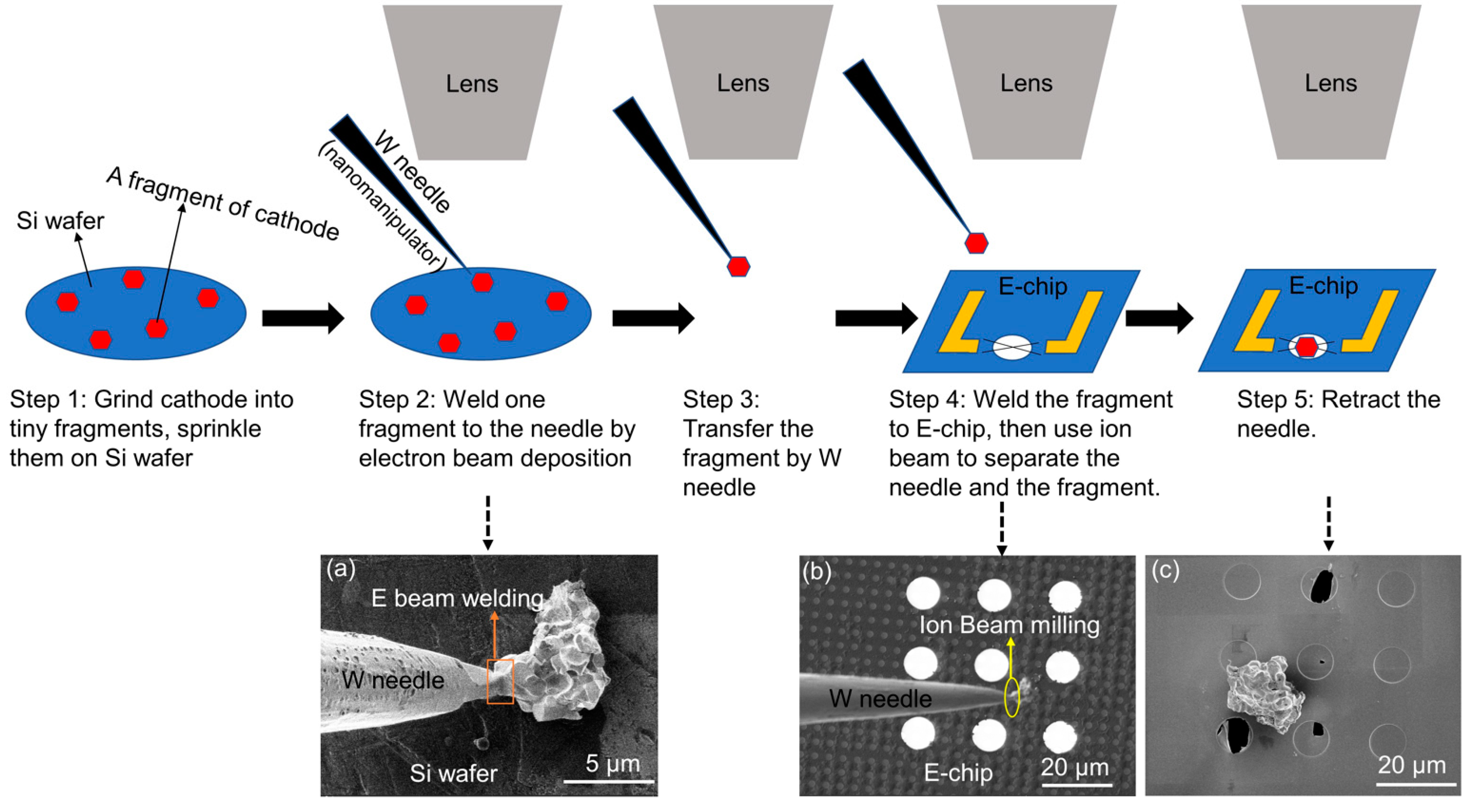
2. Materials and Methods

The materials studied in this paper were obtained from specimens that had been prepared using standard cathode processing techniques. Preliminary complementary results were presented in [39]. The initial specimen was a tungsten-based scandate pellet (fabricated by 3M Technical Ceramics, Lexington, KY, USA) that was made from a blend of 2.0 µm tungsten (W) powder and nanoscale (<50 nm diameter) Sc2O3 powder that had been mixed thoroughly. The mixture was processed using powder metallurgical methods to obtain a sintered porous pellet with a final density of 70%. This pellet was then impregnated with a 6BaO-1CaO-2Al2O3 molten ceramic mixture (1500 °C) but was not activated following this impregnation step.
Subsequent heating experiments up to an activation temperature of 1200 °C (true temperature) were instead performed in the SEM, for in situ observation of changes in material phase and morphology. To prepare specimens for in situ heating experiments, the as-impregnated cathode pellet was manually crushed and ground into tiny fragments. A portion of these particles was then dispersed on a silicon (Si) wafer and loaded into a focused ion beam and scanning electron microscope (FIB-SEM; FEI Helios G3 dual-beam system, Hillsboro, OR, USA). Utilizing a tungsten needle (nanomanipulator) in the FIB-SEM, an individual fragment from the crushed pellet was transferred from the Si wafer and attached to a MEMS heater chip (Fusion Thermal E-chip from Protochips Inc., Morrisville, NC, USA). The MEMS heater chip had a continuous silicon nitride (SiN) coating, a heating membrane area measuring 350 × 1000 µm2, and a periodic array of circular holes (8 µm diameter) that can be used for transmission electron microscopy observations (these were not performed in the current study). Electron beam welding and ion beam milling were utilized to affix and detach each cathode fragment from the tungsten needle, facilitating successful transfer and attachment of the cathode particles to the heater chip. After each fragment was loaded onto its own E-chip, electron beam deposition of tungsten was applied once more to attach the sample to the heater chip, thereby improving thermal conduction and minimizing sample vibration during the heating experiments. The process of loading and attaching an individual fragment to a heater chip is shown schematically in Figure 1.
Before heating, each fragment was characterized using SEM imaging and X-ray energy dispersive spectroscopy (EDS, Oxford Instruments X-Max 80 mm2 detector, Concord, MA, USA) in the FIB-SEM chamber. In situ heating experiments were performed under a vacuum of 10−6 to 10−7 mbar, with sample temperature controlled by “Protochips Fusion 350 v 2.1.6” software (Protochips Inc., Morrisville, NC, USA). The heating rate ranged from 0.1 to 0.3 °C/s. Once the sample reached the target temperature, it was held there for 10 to 15 min, after which it was cooled at a controlled rate of 0.1 to 0.3 °C/s. During each in situ heating experiment, SEM images and videos were recorded to document changes in morphology of the cathode fragment.

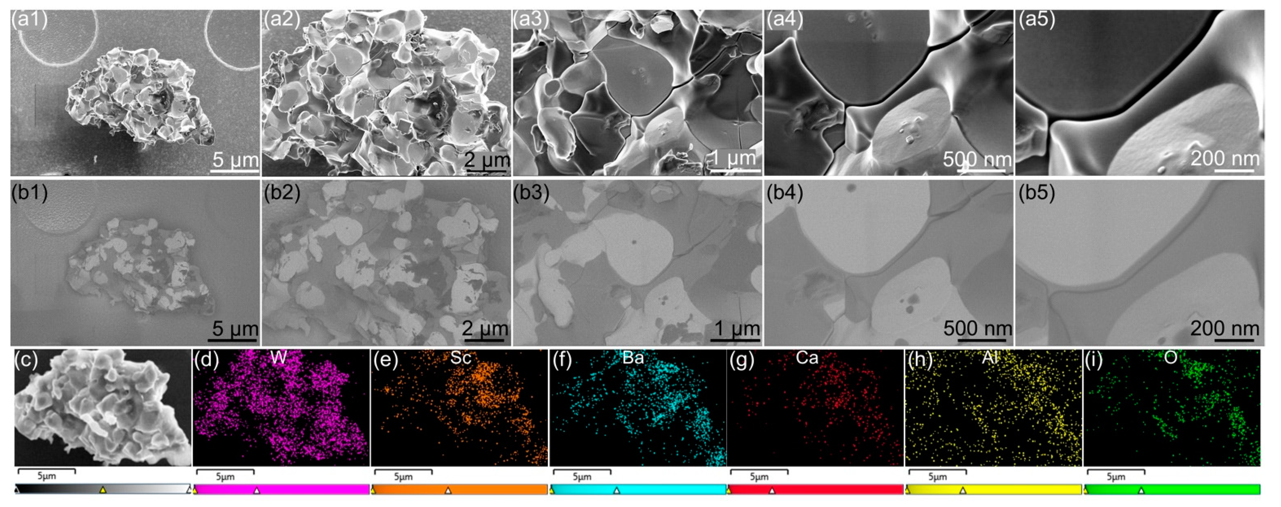
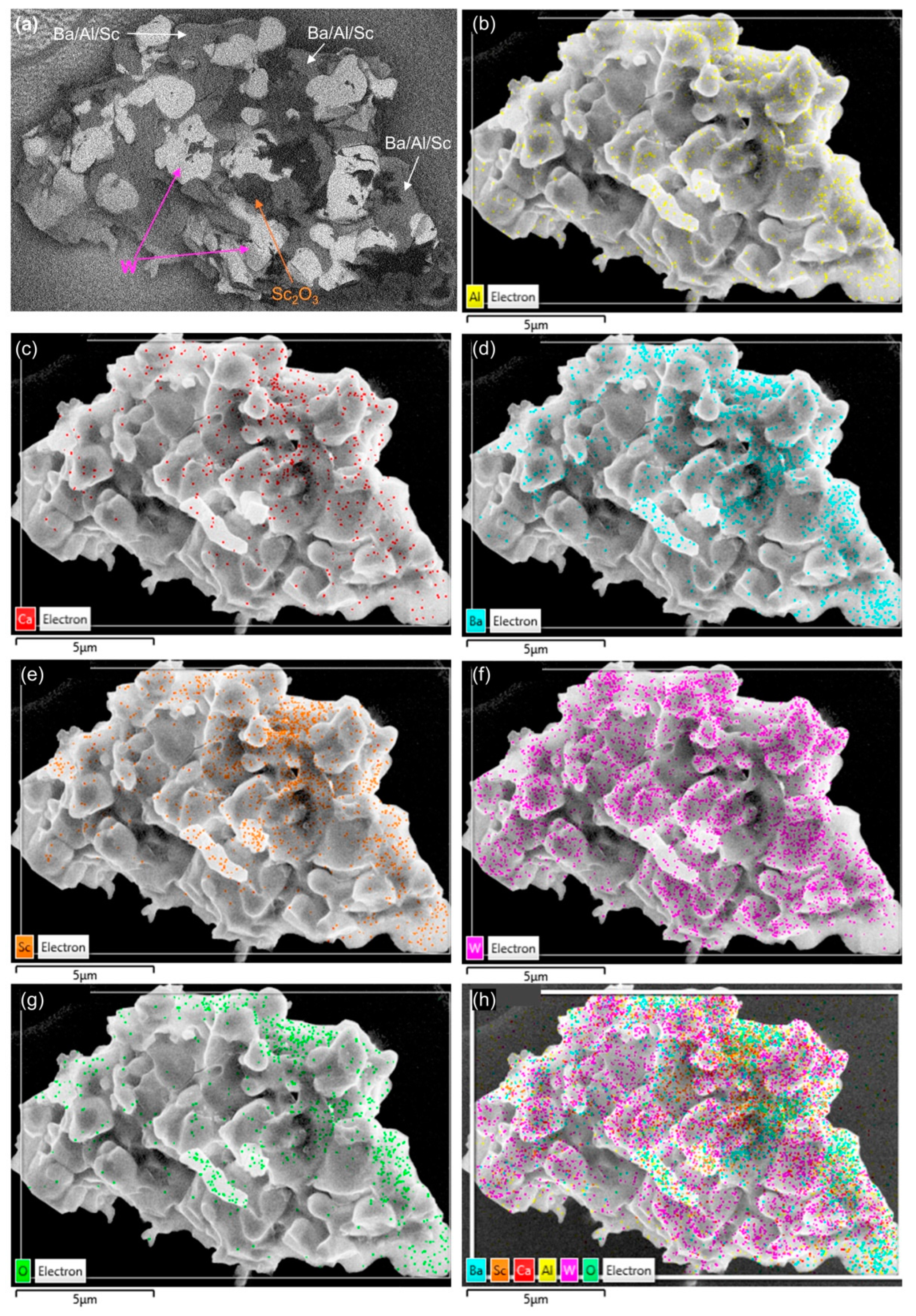
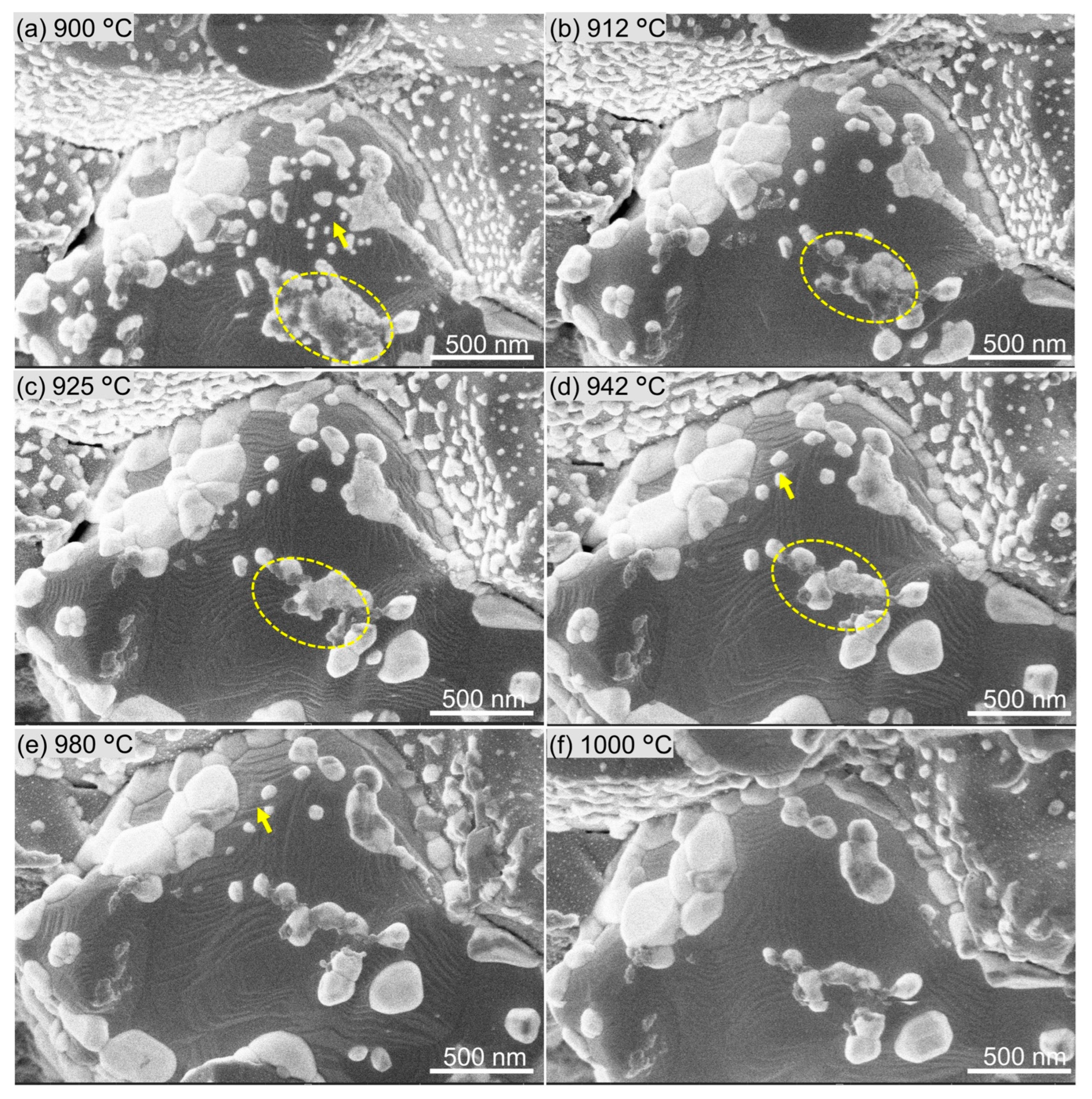
3. Results and Analysis

Figure 2 presents an analysis of the microstructure, morphology, and distribution of elements and phases in the initial fragment from the tungsten-based scandate cathode, after attachment to the SiN-coated E-chip but before the heating experiment. The secondary electron (SE) images in Figure 2(a1–a5) reveal that the fragment contains a mixture of sub-micron and micron-scale particles, some of which exhibit relatively smooth surfaces. The corresponding backscattered electron (BSE) images in Figure 2(b1–b5) indicate that most of the larger particles are tungsten, based on their relative brightness due to higher atomic number. The EDS elemental maps in Figure 2c–i suggest that the irregular-shaped regions are impregnant materials, consisting of elements including Ba, Ca, Al, O, and Sc. The lower-magnification BSE images (Figure 2(b1–b3)) suggest that the impregnant materials may exist as multiple phases, based on their difference in brightness. However, it is difficult to state this with confidence based on Figure 2 alone, so a more detailed set of observations will be presented below. It is noted that Si and N were also detected by EDS, due to the SiN coating on the E-chip, but these were not included in the maps in Figure 2.
Figure 3 presents the EDS analysis of this initial fragment from a different perspective, with EDS signal overlaid on the SE image in order to determine the distribution of elements more precisely. A BSE image of the particle is shown in Figure 3a, where the histogram and gamma of the image were adjusted using ImageJ (version 1.53e) to differentiate the gray levels more clearly. Individual elemental maps (Al, Ca, Ba, Sc, W, and O) and a composite EDS map are shown in Figure 3b–h, with the electron image in the background. Comparing the elemental maps with the BSE image (Figure 3a), it is seen that the bright grains in the BSE image can be clearly identified as W, as it has the highest atomic number (Z = 74) of all elements in this sample. Ca is difficult to identify in correlation with discrete regions of the fragment, due to its low EDS signal count (Figure 3c). Additionally, its atomic number (Z = 20) is similar to that of Sc (Z = 21), making it difficult to distinguish their oxides in a BSE image. The majority of the medium-gray (i.e., non-tungsten) regions of the fragment appears to consist of a mixed oxide containing Ba, Al, and Sc, as indicated by the white arrows in Figure 3a.
A complicating factor in this analysis is that the contrast effect for BSE imaging does not emanate solely from compositional contrast based on the average atomic number, but it can also be influenced by sample topography [42]. To mitigate this effect for the rough fragment, an in-column detector (ICD) was used for BSE imaging, reliably generating a signal at all locations of the sample and providing a true plan-view BSE image (Figure 3a) due to the location of the ICD at the top of the electron column of the FIB-SEM. However, the collection of X-rays for elemental mapping was still affected by sample surface roughness, due to the off-axis angle of the detector, meaning that EDS collection was significantly hindered in locally deep regions of the fragment. Therefore, it is difficult to correlate the gray level with the composition for every sample region visible in the BSE image. For example, the darkest regions in the BSE image (Figure 3a) should be oxide particles containing low atomic number elements (on average), but their composition cannot be determined directly from Figure 3. A further complicating factor regarding the identification of individual phases visible in the BSE image is that the impregnant oxides most likely exist as mixed phases, as a result of the impregnation process step that involves the infiltration of molten material (BaO-CaO-Al2O3) into the porous W. It is anticipated that the molten oxide dissolves some or all of the pre-existing scandia particles in the W-Sc2O3 sintered body, which could result in one or more mixed oxide phases residing in the tungsten pores after solidification. It is noted, however, that a small number of individual Sc2O3 particles appear to remain after impregnation, based on the comparison of EDS elemental maps, e.g., as indicated by the orange arrow in Figure 3a that points to a particle showing Sc but effectively no Ba or Al.
Figure 4 presents images acquired during an in situ SEM heating experiment conducted in the FIB-SEM, with a chamber pressure of 10−6 to 10−7 mbar. The fragment was heated on the E-chip to 850 °C and held there for 15 min. The initial image in Figure 4a portrays the morphology of tungsten particles and impregnant materials in a scandate cathode fragment at room temperature. As the temperature was raised to approximately 600 °C, some of the impregnant materials experienced growth and formed small features with a rod-like morphology, as indicated by the yellow arrows in Figure 4b,c. At 712 °C (Figure 4d), these and other impregnant regions underwent continued growth, changing from a rod-like shape to a set of more equiaxed, highly faceted grains, as shown in Figure 4g. As the temperature increased to 800 °C (Figure 4e), these faceted crystallites grew larger, with some appearing to grow along (and in contact with) the surface of the tungsten grain, as denoted by the yellow arrows in Figure 4h. As the temperature approached 850 °C, the impregnant materials continued to increase in size, as demonstrated in Figure 4f,i. Additionally, these grains consolidated as they grew, resulting in fewer and larger particles, which is readily apparent when comparing Figure 4g,i. Finally, no significant changes in tungsten grain morphology were observed during in situ heating experiments up to 850 °C, i.e., the W grains remained unaltered compared to their initial state at room temperature.
During in situ heating, EDS analysis of the sample was attempted, but the EDS detector was unable to obtain a measurable signal for sample temperatures above 400 °C. As a result, EDS scans and a corresponding image were recorded after the sample cooled from 850 °C to 25 °C, for the same region that was imaged in Figure 4i. As shown in the SE image of Figure 5a, the faceted crystal shapes in the impregnant material region remained unchanged from their state in Figure 4i after cooling, and the tungsten grain morphology also remained consistent with Figure 4i. It is noted that the sample view changed slightly during cooling, due to sample rotation on the E-chip as temperature decreased. However, careful inspection of Figure 4i and Figure 5a confirms that the crystallite configuration did not change. The BSE image in Figure 5b shows impregnant materials that exhibit multiple gray levels, suggesting that distinct phases may exist as a result of phase separation. Moreover, the layered EDS map in Figure 5c provides details of the elemental distribution in this sample region, revealing that strong Ba and O signals were detected throughout much of this region, except in the areas where metallic tungsten was detected (bright regions in Figure 5b). Focusing on the EDS point scan of the faceted region (Spectrum 1) in Figure 5d, it was determined that the faceted impregnant particle contains a ratio of 5.1 at.% Ba to 12.0 at.% Al, as well as other elements expected in the annealed cathode fragment. The tungsten signal is attributed to the metallic W region behind the faceted impregnant feature, which is sufficiently thin to allow the EDS interaction volume to extend beyond the faceted feature; this is consistent with previously reported findings [39]. Liu et al. [14] observed a similar result in their study of an activated scandate cathode and proposed that the impregnant phase corresponded to the compound BaAl2O4, albeit with excess O detected. The ratio of Ba to Al in the faceted feature (Spectrum 1 of Figure 5d) is approximately 1:2, which is consistent with the chemical formula BaAl2O4 and which also agrees with the measurements reported by Liu et al. [14].
An in situ heating experiment from 25 °C to 1000 °C with a surrounding pressure of 10−6 to 10−7 mbar was performed in the Helios SEM to observe another fragment (from the same scandate cathode pellet as above), with selected SE images presented in Figure 6. After reaching the target annealing temperature of 1000 °C, this sample was held for 10 min, at which point the sample started shaking, vibrating and rotating, and eventually flipped over. Comparing the morphology at 850 °C in Figure 4i with the morphologies at temperatures above 900 °C in Figure 6, it can be seen that phase separation of impregnant materials became conspicuous and impregnant faceting continued. Additionally, certain impregnant particles began to migrate and eventually formed an array of small discrete islands. At the same time, impregnant particles gradually evaporated as the temperature increased from 900 to 1000 °C, as denoted by the yellow arrows and dashed ovals in Figure 6. Finally, it was observed that nanoscale facet steps began to form on the tungsten grain surfaces.
Figure 7 presents SEM images of a fragment obtained from the same original scandate cathode pellet, at a temperature of 1200 °C and surrounding pressure of 10−6 to 10−7 mbar. Remarkably, the impregnant material particles underwent a rapid ‘boil-off’ phenomenon when the sample was held at 1200 °C for ~20 min. The completion of this boil-off process, i.e., the disappearance of the impregnant particles, occurred within 1–2 min for some particles, but took ~20 min for most particles (see Figure 7). Once all the impregnant had boiled off, no further discernible change was observed on the tungsten surfaces, even after maintaining sample temperature at 1200 °C for another 40 min.
Significant vibration and rotation of the sample were observed during heating experiments at high temperatures, e.g., 1200 °C, which resulted in some degradation of the SEM image contrast, as seen in Figure 7. Additionally, it appeared that the SiN membrane of the E-chip was damaged by the tungsten fragment during the high-temperature hold at 1200 °C, resulting in a hole in the E-chip. This may be due to a chemical reaction between W and SiN. It is noted that the reactions between the fragment and E-chip, as well as formation of a hole in the E-chip, occurred after the observations that are reported in this paper.
Additionally, in situ observations were recorded during cooling, following the heating experiments that involved maximum temperatures of 850 °C, 1000 °C, and 1200 °C. However, no meaningful changes were observed in the cathode fragments during cooling. Moreover, all E-chips developed cracks near the end of each in situ experiment, as the sample temperature decreased below ~400 °C, which in most cases prevented the sample from being preserved for further analysis after each experiment. A notable exception was the sample cooled from 850 °C and imaged as shown in Figure 5.

4. Discussion

4.1. Behavior of Impregnant Materials during Heating Experiments

The current study focused on the materials contained in a scandate dispenser cathode, which includes the ceramic mixture 6BaO-1CaO-2Al2O3 as an impregnant material infiltrated into porous tungsten, as well as nanoscale scandium oxide (Sc2O3) powder that had been mixed with W powder before sintering and was, therefore, located on the surfaces of W ligaments before infiltration of the impregnant. Through in situ heating experiments conducted on a fragment of the scandate dispenser cathode, detailed observations of impregnant material at elevated temperatures and under high vacuum conditions (10−7 to 10−6 mbar) were obtained. Figure 4 and Figure 5 demonstrate that faceted features grow out of impregnant particles at ~620 °C and these faceted features continue to develop as temperature rises.
Concurrently, there appears to be phase separation of the impregnant, with the formation of barium-aluminum oxide that exhibits a highly faceted morphology (Figure 5d). This faceting of the ceramic impregnant was not observed before the heating experiments, as seen by comparing Figure 2(a3–a5,b3–b5) and Figure 5d. Given the EDS analysis in Figure 5d, this faceted oxide appears to be BaAl2O4, consistent with previous studies [12,13,14] by Liu et. al., who described the following reaction occurring in scandate dispenser cathodes:
BaO + Al 2 O 3 BaAl 2 O 4
In a similar vein, Zhu et al. [43] reported observations of the segregation and faceting of barium oxide (BaO and BaO2) nanoparticles in Ba-containing perovskite materials, where barium oxide particles exhibited rapid growth at ~800 °C. More specifically, they found that BaO particles first became active, i.e., they exhibited incipient growth and faceting, as the temperature reached ~650 °C [43]. This is similar to the phenomenon observed in the current paper. It appears that BaO became active as it was heated to ~620 °C and then reacted according to reaction (1), causing BaAl2O4 to precipitate and grow into faceted crystals during the in situ SEM heating experiment, as shown in Figure 4.
Furthermore, with increasing temperature, the impregnant material continues to migrate on W surfaces and phase separation is apparent at 1000 °C (Figure 6). It is noted that the images in Figure 6 were obtained in SE mode, because the BSE detector was not able to record images at high temperatures. However, images obtained at room temperature after the heating experiment, e.g., Figure 5b, are consistent with the description of phase separation.

4.2. Incipient Faceting and Formation of Nanoscale Steps on W Grains

The emergence of nanoscale steps on tungsten grains was observed when the sample temperature exceeded 900 °C, as depicted in Figure 6. However, even after a temperature hold at 1200 °C for 1 h, the tungsten surfaces did not exhibit a highly faceted morphology. Full faceting would be expected during the complete activation of a scandate cathode, as described by Liu et al. [4,12,13,14,15] and Vancil et al. [44,45]. The observation of only incipient faceting activity, i.e., the formation of nanoscale steps on W surfaces as opposed to full faceting, is attributed to an artificially high amount of free surface area for the cathode fragment, in comparison to the available free surface area in a dispenser cathode pellet. The additional surface area enhances the loss or “boil-off” of impregnant material, e.g., via sublimation in the high-vacuum SEM environment. This would significantly alter the relative amounts of impregnant versus W surface area, and may change the kinetics of W surface transport and the evolution of surface morphology as W surface faceting is contingent on environmental factors and on temperature, as discussed in our prior work [38,46] and in the literature [47,48,49,50,51]. The absence of a highly faceted structure for the tungsten grains in the current study suggests incomplete activation of the scandate cathode fragment.

4.3. Scandate Dispenser Cathode Activation

To complete the standard activation process for a dispenser cathode, it must be heated to a specific temperature range (1150 to 1200 °C) for several hours [3,13,35]. Typically, heating at 1200 °C for more than 4 h is required to activate cathodes according to industry practice [35]. The activation procedure can sometimes be complex. Mantica et al. [35] emphasized the importance of employing the correct activation schedule, as it directly impacts the performance and lifespan of dispenser cathodes. In the current study, heating experiments were conducted with a temperature ramp ranging from 0.1 to 0.3 °C/s. The sample was maintained at 1200 °C for 1 h. However, it was not feasible to extend the duration at 1200 °C due to damage to the SiN membrane of the E-chip that was caused by the interaction of W and SiN at high temperature. This damage resulted in the formation of holes, rendering it impossible to continue holding the sample, thereby preventing full activation of the dispenser cathode fragment within the heating duration of the experiment.
Another possible reason that the cathode fragment was not able to be activated in this study is the high amount of free tungsten surface area that was not covered by impregnant phases. This reflects an insufficient amount of impregnant material and may indicate an inadequate ratio of impregnant to W surface area for the heated scandate cathode fragments, thereby preventing the W from forming surface facets. To activate a scandate cathode, it is necessary to have a sufficient amount of impregnant material; however, due to the use of small fragments in the current study, it was challenging to control the amount of impregnant (and ratio to W surface area). Scandate cathode activation is more complicated than simply heating the sample to a certain temperature and holding it there. Instead, it involves the careful control of material environments, e.g., infiltrating a molten impregnant into the porous tungsten-scandia body, which involves molten ceramic (impregnant) sweeping through the pores and over the W ligament surfaces, where they can react with nanoscale scandia and facilitate W mass transport to produce faceted tungsten [13].
A third potential reason for the incomplete activation of the scandate cathode fragment could be a temperature disparity between the conventional cathode activation apparatus and the in situ heating stage employed in the present study. Extensive investigations on scandate dispenser cathodes have been conducted by numerous researchers, including Liu et al. [4,12,13,14,15] and Vancil et al. [44,45], etc. However, in all of these studies, temperature was measured and reported in terms of tungsten “brightness temperature”, typically obtained using a disappearing filament optical pyrometer that continuously compares the hot specimen to a heated tungsten filament. For example, Vancil et al. [3,45] and Liu et al. [12,13] reported a knee temperature (representing the transition from temperature-limited electron emission to space-charge-limited emission) of ~800 °Cb, i.e., using tungsten brightness temperature [3] to describe their cathodes. To achieve the full activation of their dispenser cathodes, they heated in a high-vacuum environment at ~1150 °Cb (tungsten brightness temperature) [3,12,52]. Similarly, Wang et al. [53] and Busbaher et al. [54] reported the activation of their scandate cathodes at 1150 °Cb (tungsten brightness temperature) for a duration of 2 h. Additionally, most cathode activation studies report temperature in terms of tungsten brightness, including for other cathode types [28,55,56,57]. However, the difference between tungsten brightness temperature and true temperature is seldom addressed, with rare exceptions such as the study from Kordesch et al. [58] (although the equation in that particular publication may not be applicable to our current work).
The relationship between the true temperature and the brightness temperature of tungsten has been studied since 1917 [59] and can generally be calculated using the equation proposed by Rutgers et al. [60]:
1 S 1 T = 1.0410 × 10 4 log 0.92 × ε λ ,   T
In Equation (2), S represents the brightness temperature, T denotes the true temperature, ε represents the emissivity of tungsten, and λ represents the wavelength of radiation [60]. Rutgers et al. [60] provided a range of brightness temperature (S) values from 1000 to 3200 K, along with their corresponding true temperature (T) values. This approach yields an estimated true temperature of ~850 °C, corresponding to a tungsten brightness temperature of 800 °Cb. Similarly, an estimated true temperature of ~1230 °C is equivalent to a tungsten brightness temperature of 1150 °Cb. Therefore, 850 °C and 1230 °C may be more accurate and relevant temperatures with respect to scandate cathode activation. The annealing temperatures used in the current study did not quite reach the corrected temperature of 1230 °C, i.e., it is possible that the maximum temperature and/or annealing time were insufficient to induce the anticipated amount of W surface faceting. Overall, the (true) temperatures reported in the current study should be reduced by 50 to 80 °C to obtain brightness temperatures for comparison to the parameters used in industry.
Here, in situ heating experiments were conducted up to 1200 °C, as this represents the highest temperature attainable when using the E-chip. Achieving a longer duration, e.g., 1 h at 1200 °C, poses challenges for the Helios FIB-SEM. Long hold times resulted in the SE images becoming completely washed out, with no contrast or recognizable features. Only shorter-duration holds were possible, e.g., 22 min at 1200 °C (see Figure 7). Moreover, the E-chip is not designed to withstand prolonged heating periods. Thus, there remain challenges to be addressed in future research on in situ heating studies of scandate cathodes.

5. Conclusions

This paper presents a targeted series of in situ heating experiments performed using MEMS-based heater chips in a scanning electron microscope (SEM) under high vacuum conditions (10−6 to 10−7 mbar). The experiments specifically focused on the behavior of impregnated but un-activated scandate cathode fragments, leading to insightful observations regarding the growth, faceting, migration, and phase separation characteristics of these impregnant materials at intermediate temperatures relevant to cathode processing.
(1)
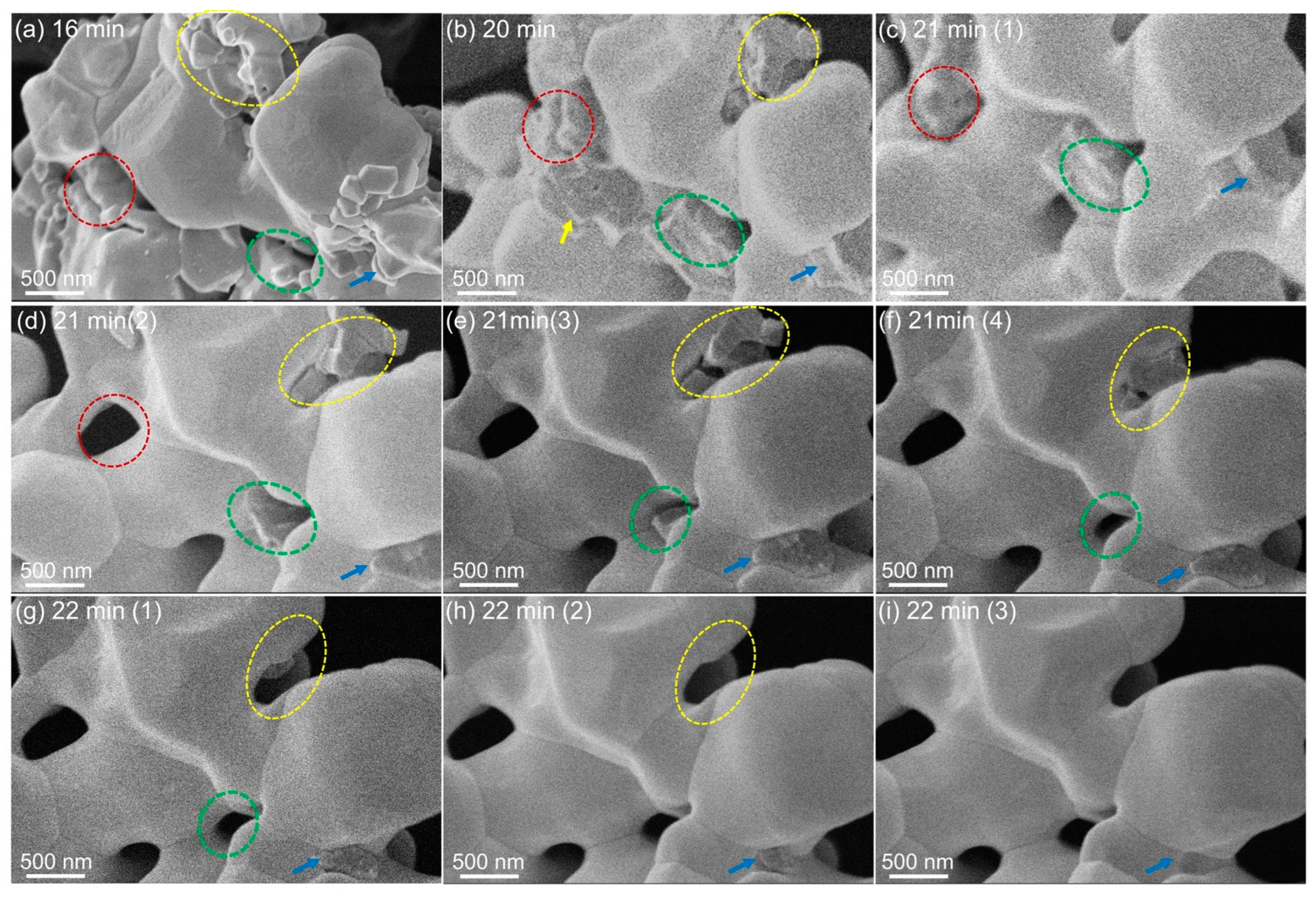
EDS analysis of faceted impregnant particles indicated they were predominantly composed of barium-containing oxides, with BaAl2O4 observed frequently.
(2)
As temperature was increased, impregnants exhibited phase separation and began to sublimate.
(3)
Concurrently, nanoscale steps emerged on tungsten surfaces, although the tungsten grains did not achieve a highly faceted morphology.
(4)
As samples approached a temperature of 1200 °C, impregnant materials underwent rapid dissipation, most likely via sublimation.
The challenges encountered during these in situ heating experiments on MEMS heater chips were acknowledged and discussed, also pointing to opportunities for further investigation into the in situ heating behavior of scandate cathodes. Moreover, the observations in the current study provide a stronger basis for understanding how the constituent materials in a dispenser cathode pellet evolve during processing. Prior studies had indicated the desired end state in which materials should exist for a high-performance scandate cathode, but it was not known how certain materials changed during thermal processing of the cathode. The results presented in this paper have filled some of that knowledge gap, specifically with respect to how ceramic impregnant materials grow and tungsten surfaces begin to facet at elevated temperature in this environment. More work remains, and future studies will enhance the community’s understanding of scandate cathode materials behavior, which should support academic scientists and industry engineers in their efforts to improve the design and performance of dispenser cathodes.

Supplementary Materials

The following supporting information can be downloaded at: https://www.mdpi.com/article/10.3390/cryst14100840/s1, Figure S1: EDS elemental mapping of the sample prior to heating in the SEM; Figures S2 and S3: original EDS elemental point scan and maps of the sample cooled from 850 °C; Tables S1–S3: Heating schedules for cathode particles ramped to 850, 1000, 1200 °C, respectively.

Author Contributions

Conceptualization, H.B. and T.J.B.; Formal analysis, H.B.; Funding acquisition, T.J.B.; Investigation, H.B.; Methodology, H.B. and T.J.B.; Project administration, T.J.B.; Writing—original draft, H.B.; Writing—review and editing, H.B. and T.J.B. All authors have read and agreed to the published version of the manuscript.

Funding

This work was financially supported by the Defense Advanced Research Projects Agency (DARPA) Innovative Vacuum Electronics Science and Technology (INVEST) program, under grant number N66001-16-1-4041. The views, opinions, and/or findings expressed are those of the author(s) and should not be interpreted as representing the official views or policies of the Department of Defense or the U.S. Government. This work was performed in part at the U.K. Electron Microscopy Center, a member of the National Nanotechnology Coordinated Infrastructure (NNCI), which is supported by the National Science Foundation (NNCI-2025075).

Data Availability Statement

Data are contained within the article or Supplementary Materials.

Acknowledgments

In the initial stages of preparing this paper, the authors used ChatGPT to paraphrase and improve readability. After using this tool, the authors reviewed, edited and completely reworked the content. We take full responsibility for the content of the publication.

Conflicts of Interest

The authors declare no conflicts of interest.

References

  1. Bugaris, D.E.; Goggin, C.; Zhang, X.; Balk, J.; Busbaher, D.; Tucek, J. High-Performance Scandate Cathode. In Proceedings of the 2019 International Vacuum Electronics Conference (IVEC), Busan, Republic of Korea, 28 April–1 May 2019; pp. 1–2. [Google Scholar]
  2. Gao, J.Y.; Yang, Y.F.; Zhang, X.K.; Li, S.L.; Hu, P.; Wang, J.S. A review on recent progress of thermionic cathode. Tungsten 2020, 2, 289–300. [Google Scholar] [CrossRef]
  3. Kirkwood, D.M.; Gross, S.J.; Balk, T.J.; Beck, M.J.; Booske, J.; Busbaher, D.; Jacobs, R.; Kordesch, M.E.; Mitsdarffer, B.; Morgan, D.; et al. Frontiers in Thermionic Cathode Research. IEEE Trans. Electron Devices 2018, 65, 2061–2071. [Google Scholar] [CrossRef]
  4. Liu, X.; Vancil, B.K.; Durham, D.B.; Ogletree, D.F.; Barnard, E.S.; Balk, T.J. Observation of Ultrathin Sc-Containing Surface Layer on Life-Tested Scandate Cathodes. IEEE Trans. Electron Devices 2023, 70, 2876–2882. [Google Scholar] [CrossRef]
  5. Gong, T.; Zhou, Y.; Zhang, Z.; Xu, L.; Zhou, X.; Fu, H. Environmental Stability of 612-aluminate with Different Phase Structures. In Proceedings of the 2023 24th International Vacuum Electronics Conference (IVEC), Chengdu, China, 25–28 April 2023; pp. 1–2. [Google Scholar]
  6. Sun, J.; Gao, J.; Yang, Y.; Zhang, R.; Liu, H.; Wang, J. Investigation on Scadium Thin Films on Dispenser Cathodes. In Proceedings of the 2023 24th International Vacuum Electronics Conference (IVEC), Chengdu, China, 25–28 April 2023; pp. 1–2. [Google Scholar]
  7. Cai, Y.; Yang, Y.; Liu, H.; Sun, J.; Li, Z.; Zhou, W.; Hu, Y.; Wang, J. Synthesis of impregnants for dispenser cathodes via homogeneous-lyophilization: Phase structure, optical response and emission property of four aluminates. Ceram. Int. 2024, 50, 11341–11350. [Google Scholar] [CrossRef]
  8. Lai, C.; Guo, G.; Dong, L.; Cai, Y.; Zhou, F.; Zheng, Z.; Yang, Y.; Zhou, W.; Wang, J. The effects of aluminate compounds on the free Ba generation and electron emission performance of dispenser cathode. Ceram. Int. 2024, in press. [CrossRef]
  9. Shang, Y.; Zheng, Q.; Cao, Y.; Hu, J.; Fu, H.; Luo, Y.; Yang, D. Effect of sintering atmospheres on the structure and properties of the 612 type barium-calcium-aluminate for the dispenser cathodes. Ceram. Int. 2019, 45, 14816–14820. [Google Scholar] [CrossRef]
  10. Ives, R.L.; Falce, L.R.; Miram, G.; Collins, G. Controlled-Porosity Cathodes for High-Current-Density Applications. IEEE Trans. Plasma Sci. 2010, 38, 1345–1353. [Google Scholar] [CrossRef]
  11. Swartzentruber, P.D. Microstructure and Work Function of Dispenser Cathode Coatings: Effects on Thermionic Emission. Ph.D. Dissertation, University of Kentucky, Lexington, KY, USA, 2014. [Google Scholar]
  12. Liu, X.; Zhou, Q.; Maxwell, T.L.; Vancil, B.K.; Beck, M.J.; Balk, T.J. Scandate cathode surface characterization: Emission testing, elemental analysis and morphological evaluation. Mater. Charact. 2019, 148, 188–200. [Google Scholar] [CrossRef]
  13. Liu, X. Characterization of Nanostructure, Materials, and Electron Emission Performance of Next-Generation Thermionic Scandate Cathodes. Ph.D. Dissertation, University of Kentucky, Lexington, KY, USA, 2019. [Google Scholar]
  14. Liu, X.; Vancil, B.K.; Beck, M.J.; Balk, T.J. Near-Surface Material Phases and Microstructure of Scandate Cathodes. Materials 2019, 12, 636. [Google Scholar] [CrossRef]
  15. Zhou, Q.; Liu, X.; Maxwell, T.; Vancil, B.; Balk, T.J.; Beck, M.J. BaxScyOz on W (0 0 1), (1 1 0), and (1 1 2) in scandate cathodes: Connecting to experiment via μO and equilibrium crystal shape. Appl. Surf. Sci. 2018, 458, 827–838. [Google Scholar] [CrossRef]
  16. Kapustin, V.; Li, I.; Shumanov, A.V.; Lebedinskii, Y.Y.; Zablotskii, A.V.E. Physical operating principles of scandate cathodes for microwave devices. Tech. Phys. 2017, 62, 116–126. [Google Scholar] [CrossRef]
  17. Shukla, S.; Singh, A.; Barik, R. Synthesis of Rhenium–Scandia doped tungsten nanoparticles for shrinkage investigation. J. Sol-Gel Sci. Technol. 2020, 95, 384–392. [Google Scholar] [CrossRef]
  18. Barik, R.K.; Sattorov, M.; Park, G.-S. Cathode Technologies for Terahertz Source. In Advances in Terahertz Source Technologies; Jenny Stanford Publishing: Singapore, 2024; pp. 665–700. [Google Scholar]
  19. Zheng, Q.; Huang, Z.; Shang, Y.; Liu, M.; Li, Y.; Luo, Y.; Fu, H. Single-phase (Ba,Ca)2ScAlO5 impregnant for dispenser cathodes with enhanced thermionic emission performance. Ceram. Int. 2021, 47, 1632–1639. [Google Scholar] [CrossRef]
  20. Sun, J.; Yang, Y.; Dong, L.; Liu, Z.; Liu, P.; Cai, Y.; Liu, H.; Wang, J. Vacuum evaporation synthesizing Sc film layer and elucidation of near-surface Ba-O-Sc electronic configuration for dispenser cathode. Appl. Surf. Sci. 2024, 679, 161241. [Google Scholar] [CrossRef]
  21. Li, N.; Zhang, K.; Feng, J. Effect of Sr-Doping on the Emission-Active Materials of Scandate Cathodes. IEEE Trans. Electron Devices 2023, 70, 5883–5889. [Google Scholar] [CrossRef]
  22. Wang, J.; Li, L.; Liu, W.; Wang, Y.; Wang, Y.; Zhou, M. Sc2O3–W matrix impregnated cathode with spherical grains. J. Phys. Chem. Solids 2008, 69, 2103–2108. [Google Scholar] [CrossRef]
  23. Lai, C.; Wang, J.; Zhou, F.; Liu, W.; den Engelsen, D.; Miao, N. Emission and evaporation properties of 75 at.% Re-25 at.% W mixed matrix impregnated cathode. Appl. Surf. Sci. 2018, 427, 874–882. [Google Scholar] [CrossRef]
  24. Krachkovskaya, T.; Storublev, A.; Sakhadji, G.; Emelyanov, A. Performance Investigation for Nanocarbon Modified Dispenser Cathode. J. Russ. Univ. Radioelectron. 2018, 4, 57–63. [Google Scholar] [CrossRef]
  25. Ao, B.; Zheng, Q.; Yan, R.; Luo, Y. Effect of Surface Features on Emission Properties of Impregnated Scandate Dispenser Cathode. In Proceedings of the 2023 24th International Vacuum Electronics Conference (IVEC), Chengdu, China, 25–28 April 2023; pp. 1–2. [Google Scholar]
  26. Gaertner, G.; Vancil, B.K. Electron Emission Model of Ba Dispenser Scandate Cathodes Based on the Beamlet Effect. e-J. Surf. Sci. Nanotechnol. 2024, 22, 179–187. [Google Scholar] [CrossRef]
  27. Gharaati, A.; Mardani, D. Fabrication and enhancement of a new high-current density scandate electron emitter for a pulsed Pierce electron gun. Eur. Phys. J. Plus 2022, 137, 615. [Google Scholar] [CrossRef]
  28. Zheng, Q.; Gong, T.; Wu, F.; Ilyas, N.; Huang, Z.; Li, Y.; Luo, Y.; Fu, H. Effect of Sc2O3 addition on the phase composition and electron emission performance of Co-precipitated aluminates for impregnated cathodes. Ceram. Int. 2021, 47, 18831–18837. [Google Scholar] [CrossRef]
  29. Zhao, J.; Gamzina, D.; Li, N.; Li, J.; Spear, A.G.; Barnett, L.; Banducci, M.; Risbud, S.; Luhmann, N.C. Scandate dispenser cathode fabrication for a high-aspect-ratio high-current-density sheet beam electron gun. IEEE Trans. Electron Devices 2012, 59, 1792–1798. [Google Scholar] [CrossRef]
  30. Lu, Z.; Yin, S.; Zhang, Z.; Ren, F.; Lv, X. Study on Low-Temperature Emission Performance of Scandate Cathode with Micro-Blade-Type Arrays. Materials 2019, 13, 100. [Google Scholar] [CrossRef] [PubMed]
  31. Gao, J.; Liu, P.; Wang, J.; Zhang, R.; Yang, Y.; Zhou, W.; Liu, H.; Sun, J. The effect of Ir and Sc on the emission capacity of W-Ir matrix scandate cathodes prepared via a novel in situ method. Acta Mater. 2023, 261, 119400. [Google Scholar] [CrossRef]
  32. Zhou, Y.; Gong, T.; Wu, M.; Xu, L.; Fu, H. Thermionic Emission Capability of the Ba–Sc–Al–O Compound Synthesized by High-Temperature Solid-State Process. IEEE Trans. Electron Devices 2023, 70, 1294–1298. [Google Scholar] [CrossRef]
  33. Wang, M.; Hu, K.; Wu, R.; Khanlari, K.; Zhang, F.; Lin, B. Effect of tungsten powder particle shape on the emission properties of the barium tungsten cathode. Adv. Powder Technol. 2023, 34, 104133. [Google Scholar] [CrossRef]
  34. Mantica, A.M.; Detisch, M.J.; Balk, T.J. Thermionic Emission Characterization of M-Type Cathodes Using Kelvin Probe in an Ultra-High Vacuum Environment. IEEE Trans. Electron Devices 2023, 70, 2864–2871. [Google Scholar] [CrossRef]
  35. Mantica, A. Surface Properties, Work Function, and Thermionic Electron Emission Characterization of Materials for Next-Generation Dispenser Cathodes. Ph.D. Dissertation, University of Kentucky, Lexington, KY, USA, 2023. [Google Scholar]
  36. Podor, R.; Le Goff, X.; Lautru, J.; Brau, H.P.; Barreau, M.; Carrier, X.; Mendonca, J.; Nogues, D.; Candeias, A. Direct Observation of the Surface Topography at High Temperature with SEM. Microsc. Microanal. 2020, 26, 397–402. [Google Scholar] [CrossRef]
  37. Gregori, G.; Kleebe, H.-J.; Siegelin, F.; Ziegler, G. In situ SEM imaging at temperatures as high as 1450 °C. Microscopy 2002, 51, 347–352. [Google Scholar]
  38. Bai, H.; Briot, N.J.; Beck, M.; Balk, T.J. Crystallographic Faceting of Bulk Tungsten Surfaces Observed During In Situ Heating in an Environmental Scanning Electron Microscope. Mater. Charact. 2024, 212, 113925. [Google Scholar] [CrossRef]
  39. Bai, H.; Balk, T.J. Observations of Temperature-Induced Material Transformations in Impregnated Scandate Cathode Samples During in situ Heating in the SEM. In Proceedings of the 2022 23rd International Vacuum Electronics Conference (IVEC), Monterey, CA, USA, 25–29 April 2022; pp. 238–239. [Google Scholar]
  40. Howe, J.; Walker, L.; Allard, L.; Demers, H. Early Experiments with a New In Situ SEM Heating Technology. Microsc. Microanal. 2017, 17, 432–433. [Google Scholar] [CrossRef]
  41. Mujin, M.; Nakamura, M.; Matsumoto, M. In-situ FE-SEM observation of the growth behaviors of Fe particles at magmatic temperatures. J. Cryst. Growth 2021, 560–561, 126043. [Google Scholar] [CrossRef]
  42. Leng, Y. Materials Characterization: Introduction to Microscopic and Spectroscopic Methods; John Wiley & Sons: Hoboken, NJ, USA, 2013. [Google Scholar]
  43. Zhu, Y.; Liu, D.; Jing, H.; Zhang, F.; Zhang, X.; Hu, S.; Zhang, L.; Wang, J.; Zhang, L.; Zhang, W. Oxygen activation on Ba-containing perovskite materials. Sci. Adv. 2022, 8, eabn4072. [Google Scholar] [CrossRef] [PubMed]
  44. Vancil, B.; Brodie, I.; Lorr, J.; Schmidt, V. Scandate dispenser cathodes with sharp transition and their application in microwave tubes. IEEE Trans. Electron Devices 2014, 61, 1754–1759. [Google Scholar] [CrossRef]
  45. Vancil, B.; Jones, D.; Kleschuk, M.; Schmidt, V.; Vancil, A.; Ohlinger, W.; Green, M. Recent Progress on Scandate Cathodes. In Proceedings of the 2020 IEEE 21st International Conference on Vacuum Electronics (IVEC), Monterey, CA, USA, 19–22 October 2020; pp. 81–82. [Google Scholar]
  46. Bai, H.; Maxwell, T.L.; Kordesch, M.E.; Balk, T.J. Physical vapor deposition and thermally induced faceting of tungsten nanoparticles. Mater. Charact. 2023, 198, 112724. [Google Scholar] [CrossRef]
  47. Acsente, T.; Negrea, R.F.; Nistor, L.C.; Matei, E.; Grisolia, C.; Birjega, R.; Dinescu, G. Tungsten nanoparticles with controlled shape and crystallinity obtained by magnetron sputtering and gas aggregation. Mater. Lett. 2017, 200, 121–124. [Google Scholar] [CrossRef]
  48. Togaru, M.; Sainju, R.; Zhang, L.; Jiang, W.; Zhu, Y. Direct observation of tungsten oxidation studied by in situ environmental TEM. Mater. Charact. 2021, 174, 111016. [Google Scholar] [CrossRef]
  49. Yu, H.; Das, S.; Liu, J.; Hess, J.; Hofmann, F. Surface terraces in pure tungsten formed by high temperature oxidation. Scr. Mater. 2019, 173, 110–114. [Google Scholar] [CrossRef]
  50. Szczepkowicz, A.; Bryl, R. Observation of vertex-rounding transition for a crystal in equilibrium: Oxygen-covered tungsten. Phys. Rev. B 2005, 71, 113416. [Google Scholar] [CrossRef]
  51. Szczepkowicz, A.; Bryl, R. From hill-and-valley faceting to global faceting of a crystal: Oxygen-covered tungsten. Surf. Sci. 2004, 559, L169–L172. [Google Scholar] [CrossRef]
  52. Kresse, R.; Baudis, U.; Jäger, P.; Riechers, H.H.; Wagner, H.; Winkler, J.; Wolf, H.U. Barium and barium compounds. In Ullmann’s Encyclopedia of Industrial Chemistry; Wiley-VCH Verlag GmbH & Co.: Weinheim, Germany, 2000. [Google Scholar]
  53. Wang, Y.; Wang, J.; Liu, W.; Zhang, X.; Li, L. Emission mechanism of high current density scandia-doped dispenser cathodes. J. Vac. Sci. Technol. B Nanotechnol. Microelectron. Mater. Process. Meas. Phenom. 2011, 29, 04E106. [Google Scholar] [CrossRef]
  54. Busbaher, D.; Zhao, J.; Gamzina, D.; Luhmann, N.C. Performance comparison between sintered tungsten dispenser cathodes and nano-composite scandate dispenser cathodes. In Proceedings of the 2013 IEEE 14th International Vacuum Electronics Conference (IVEC), Paris, France, 21–23 May 2013; pp. 1–2. [Google Scholar]
  55. Huang, Z.; Wu, F.; Zheng, Q.; Xiong, H.; Fang, J.; Liu, M.; Yan, R.; Luo, Y.; Ilyas, N.; Fu, H. Structure and emission properties of barium calcium aluminates synthesized by room-temperature solid-state reaction approach. Mater. Chem. Phys. 2021, 263, 124418. [Google Scholar] [CrossRef]
  56. Kordesch, M.; Vaughn, J.; Wan, C.; Jamison, K. Model scandate cathodes investigated by thermionic emission microscopy. In Proceedings of the 2010 8th International Vacuum Electron Sources Conference and Nanocarbon, Nanjing, China, 14–16 October 2010; pp. 41–42. [Google Scholar]
  57. Kordesch, M.E.; Wan, C. Barium de-wetting and thermionic emission from Ba on W. In Proceedings of the 2013 26th International Vacuum Nanoelectronics Conference (IVNC), Roanoke, VA, USA, 8–12 July 2013; pp. 1–2. [Google Scholar]
  58. Vaughn, J.M.; Wan, C.; Jamison, K.D.; Kordesch, M.E. Thermionic electron emission microscopy of metal-oxide multilayers on tungsten. IBM J. Res. Dev. 2011, 55, 14:11–14:16. [Google Scholar] [CrossRef]
  59. Worthing, A. The true temperature scale of tungsten and its emissive powers at incandescent temperatures. Phys. Rev. 1917, 10, 377. [Google Scholar] [CrossRef]
  60. Rutgers, G.A.W.; De Vos, J.C. Relation between brightness, temperature, true temperature and colour temperature of tungsten. Luminance of tungsten. Physica 1954, 20, 715–720. [Google Scholar] [CrossRef]
Figure 1. Schematic of the procedure for loading a cathode fragment sample onto a MEMS-based E-chip for in situ heating in the SEM. Steps 1 to 5 involve the selection and transfer process from a Si wafer to the heater chip. (ac) SEM images corresponding to steps 2, 4, and 5, illustrating key transfer steps including attachment and detachment of the cathode fragment and W needle.
Crystals 14 00840 g001
Figure 2. A fragment from an impregnated tungsten-based scandate cathode, after it was attached to the SiN-coated E-chip but before the sample was heated. (a1a5) Secondary electron images of the fragment. (b1b5) BSE images corresponding to (a1a5), respectively. (c) Electron image of the region selected for EDS analysis and elemental mapping, with individual maps for (d) W, (e) Sc, (f) Ba, (g) Ca, (h) Al, and (i) O.
Crystals 14 00840 g002
Figure 3. (a) BSE image of scandate dispenser cathode fragment prior to heating, along with EDS elemental maps overlaid on SE image for (b) Al, (c) Ca, (d) Ba, (e) Sc, (f) W, and (g) O. (h) Composite elemental map (on SE image) showing all elements and indicating mixed oxide phases (Ba/Al/Sc).
Crystals 14 00840 g003
Figure 4. Secondary electron SEM images of the sample during in situ annealing to 850 °C: (a) 25 °C; (b) 621 °C, and (c) higher magnification view of the area in yellow box in (b), showing the emergence of nanoscale rod-like features; (d) 712 °C; (e) 800 °C; (f) 850 °C; (g), (h), and (i) are higher magnification views of the areas in yellow boxes in (d), (e), and (f), respectively. These show the continued growth and consolidation of impregnant oxide crystallites, as indicated by yellow arrows.
Crystals 14 00840 g004
Figure 5. Micrographs and the corresponding EDS analysis of the scandate cathode fragment after it had cooled from 850 °C to 25 °C. (a) Secondary electron (SE) image of the scandate cathode fragment, and (b) backscattered electron (BSE) image of the same region. A layered EDS map of this region is presented in (c), and an EDS point analysis of faceted impregnant material is shown in (d) for the location labeled as Spectrum 1 in image (a).
Crystals 14 00840 g005
Figure 6. SE images showing the evolution of surface morphology as the sample nears the annealing temperature of 1000 °C, under a surrounding pressure of 10−6 to 10−7 mbar. (a) 900 °C, (b) 912 °C, (c) 925 °C, (d) 942 °C, (e) 980 °C, and (f) 1000 °C. In these images, the tungsten grains are dark gray, while the surface oxide particles are relatively bright.
Crystals 14 00840 g006
Figure 7. SE images recorded at different times while a cathode fragment was held at 1200 °C under a surrounding pressure of 10−6 to 10−7 mbar: (a) 16 min, (b) 20 min, (cf) 21 min, and (gi) 22 min. Four impregnant material particles at different locations in the sample are indicated by red, yellow, and green dashed ovals and the blue arrow in (a), and all these particles gradually disappeared during the high-temperature hold, which can be seen by considering the sequence of dashed ovals and the arrow in image frames (bi). The impregnant particle indicated by the blue arrow in (a) shrank significantly but did not disappear entirely within the first 22 min of this heating experiment.
Crystals 14 00840 g007
Disclaimer/Publisher’s Note: The statements, opinions and data contained in all publications are solely those of the individual author(s) and contributor(s) and not of MDPI and/or the editor(s). MDPI and/or the editor(s) disclaim responsibility for any injury to people or property resulting from any ideas, methods, instructions or products referred to in the content.

