Article

Surface Modification of Bi2Te3 Nanoplates Deposited with Tin, Palladium, and Tin/Palladium Using Electroless Deposition

1
Department of Materials Science, Tokai University, 4-1-1, Kitakaname, Hiratsuka 259-1292, Japan
2
Department of Mechanical Engineering, Kobe City College of Technology, 8-3, Gakuen-Higashimachi, Nishi-ku, Kobe 651-2194, Japan
*
Author to whom correspondence should be addressed.
Crystals 2024, 14(2), 132; https://doi.org/10.3390/cryst14020132
Submission received: 29 December 2023 / Revised: 24 January 2024 / Accepted: 26 January 2024 / Published: 28 January 2024
(This article belongs to the Special Issue Advances in Thermoelectric Materials 2023-2024)

Abstract

:
Surface-modified nanoplate-shaped thermoelectric materials can achieve good thermoelectric performance. Herein, single-crystalline Bi2Te3 nanoplates with regular hexagonal shapes were prepared via solvothermal techniques. Surface modification was performed to deposit different metals onto the nanoplates using electroless deposition. Nanoparticle-shaped tin (Sn) and layer-shaped palladium (Pd) formed on the Bi2Te3 nanoplates via electroless deposition. For the sequential deposition of Sn and Pd, the surface morphology was mostly the same as that of the Sn-Bi2Te3 nanoplates. To assess the thermoelectric properties of the nanoplates as closely as possible, they were compressed into thin bulk shapes at 300 K. The Sn-Bi2Te3 and Sn/Pd-Bi2Te3 nanoplates exhibited the lowest lattice thermal conductivity of 1.1 W/(m·K), indicating that nanoparticle-shaped Sn facilitated the scattering of phonons. By contrast, the Pd-Bi2Te3 nanoplates exhibited the highest electrical conductivity. Thus, the highest power factor (15 μW/(m∙K2)) and dimensionless ZT (32 × 10−3) were obtained for the Pd-Bi2Te3 nanoplates. These thermoelectric properties were not as high as those of the sintered Bi2Te3 samples; however, this study revealed the effect of different metal depositions on Bi2Te3 nanoplates for improving thermoelectric performance. These findings offer venues for improving thermoelectric performance by sintering nanoplates deposited with appropriate metals.

1. Introduction

With the development of wireless sensor networks for the Internet of Things (IoT), securing a power supply for sensors has become a major issue [1]. Therefore, energy harvesting has received considerable attention [2]. These methods convert environmental energy, including light [3,4], vibration [5,6], heat [7,8], and electromagnetic waves [9,10], into electrical energy. Among the different types of environmental energy, thermal energy is the most accessible, owing to its ubiquity; electrical energy can be obtained from it using a thermoelectric generation system. The performance of thermoelectric generation depends directly on the properties of the thermoelectric materials. The main thermoelectric properties are the power factor, PF, and the dimensionless figure of merit, ZT, which are expressed as PF = σS2 and ZT = σS2T/κ, respectively, where σ, S, T, and κ are the electrical conductivity, Seebeck coefficient, absolute temperature, and thermal conductivity, respectively.
Theoretical and experimental studies of thermoelectricity began in earnest in the 1950s [11], and various structures of thermoelectric generators have since been proposed [12,13,14,15,16]. Various thermoelectric materials have been considered, including inorganic and organic materials [17,18,19,20,21,22,23]. However, despite these efforts, the best-performing materials at temperatures of approximately 300 K have been bismuth-telluride-based alloys developed in the 1950s [24,25,26,27,28,29,30]. These alloys have hexagonal unit cells, and the lattice constant along the c-axis is almost seven times greater than that along the a- or b-axis, contributing to the significant anisotropic thermoelectric properties of the material. These alloys exhibit properties of an indirect-transition-type semiconductor with a band gap ranging from 0.1 to 0.2 eV. The typical single-crystalline Bi2Te3 bulk exhibited a ZT of approximately 0.8 [31]. Therefore, when thermoelectric generators are used to power wireless sensors, bismuth-telluride-based alloys are the most practical. However, their material performance is not sufficient to power wireless sensors, requiring further performance improvements. One approach to improving material performance is nanostructuring, which can lower thermal conductivity owing to phonon scattering and high Seebeck coefficient, which are due to lower dimensionality [32]. To this end, various nanostructured bismuth-telluride-based alloys have been developed, including superlattices [33,34], nanocrystals [35,36,37,38], nanoparticles [39,40,41], and nanoplates [42,43,44]. In superlattices, Venkatasubramanian et al. fabricated the p-type Bi2Te3/Sb2Te3 superlattices using metal–organic chemical vapor deposition and achieved a ZT of 2.4 at 300 K [33]. In nanocrystals, Poudel et al. fabricated bismuth antimony telluride bulk alloys made by hot-pressing nanoparticles and achieved a ZT of 1.4 at 373 K [35]. Wu et al. fabricated nanoporous (00l)-oriented Bi2Te3 nanoplates using a facile process combining chemical and physical methods, including annealing and a reaction-engineered solution method, and the estimated ZT was larger than 1.2 at 300 K [44]. In particular, nanoplates have excellent geometries that can be both nanostructured and low-dimensional. Because nanoplates are extremely thin (tens of nanometers) compared with their diameter, they can be considered two-dimensional structures. Therefore, the synthesis of bismuth-telluride-based alloy nanoplates and the evaluation of their thermoelectric properties have been actively investigated [45,46,47,48,49]. Nanocomposites of nanoplates with other materials have also been developed [50,51,52,53,54].
Recently, studies have been conducted to further improve the performance of nanoplates. One approach is the surface modification of nanoplates with different materials [55,56]. Zheng et al. fabricated Au-Sb2Te3 nanoplates with a beneficial interface barrier and high phonon scattering, resulting in synergistically optimal electrical and thermal properties [57]. In our previous study, tin nanoparticles were deposited on the surface of a Bi2Te3 nanoplate using electroless deposition, which reduced the lattice thermal conductivity [58]. When different materials were deposited on the surfaces of nanoplates, the crystal growth modes differed depending on the lattice matching and interfacial free energy [59]. Therefore, the morphology of the nanoplate surface varies depending on the type of material deposited on its surface, affecting its thermoelectric performance.
In this study, we prepared Bi2Te3 nanoplates via solvothermal techniques and deposited different metals (tin (Sn), palladium (Pd), and Sn/Pd) on the nanoplate surface using electroless deposition. Sn and Pd have been typically used in electroless deposition, exhibiting different deposition modes [60]. In addition, the magnitude of diffusion in Bi2Te3 is different for Sn and Pd. Sn tends to diffuse into Bi2Te3, while Pd tends to remain on the Bi2Te3 surface [61]. Therefore, different Bi2Te3 surface structures can be fabricated by using Sn and Pd, and the difference can be reflected in the thermoelectric performance. Their structural and thermoelectric properties were examined using various analytical techniques. The surface morphology of the nanoplates depended on the deposited metal. To measure the thermoelectric properties of the nanoplates, the nanoplate assemblies were compressed into thin bulk shapes. The thermoelectric properties of the bulk samples varied depending on the metal type and surface morphology of the nanoplates. Finally, we discuss the different modes of crystal growth on the nanoplates depending on the metal type and their effect on the thermoelectric properties.

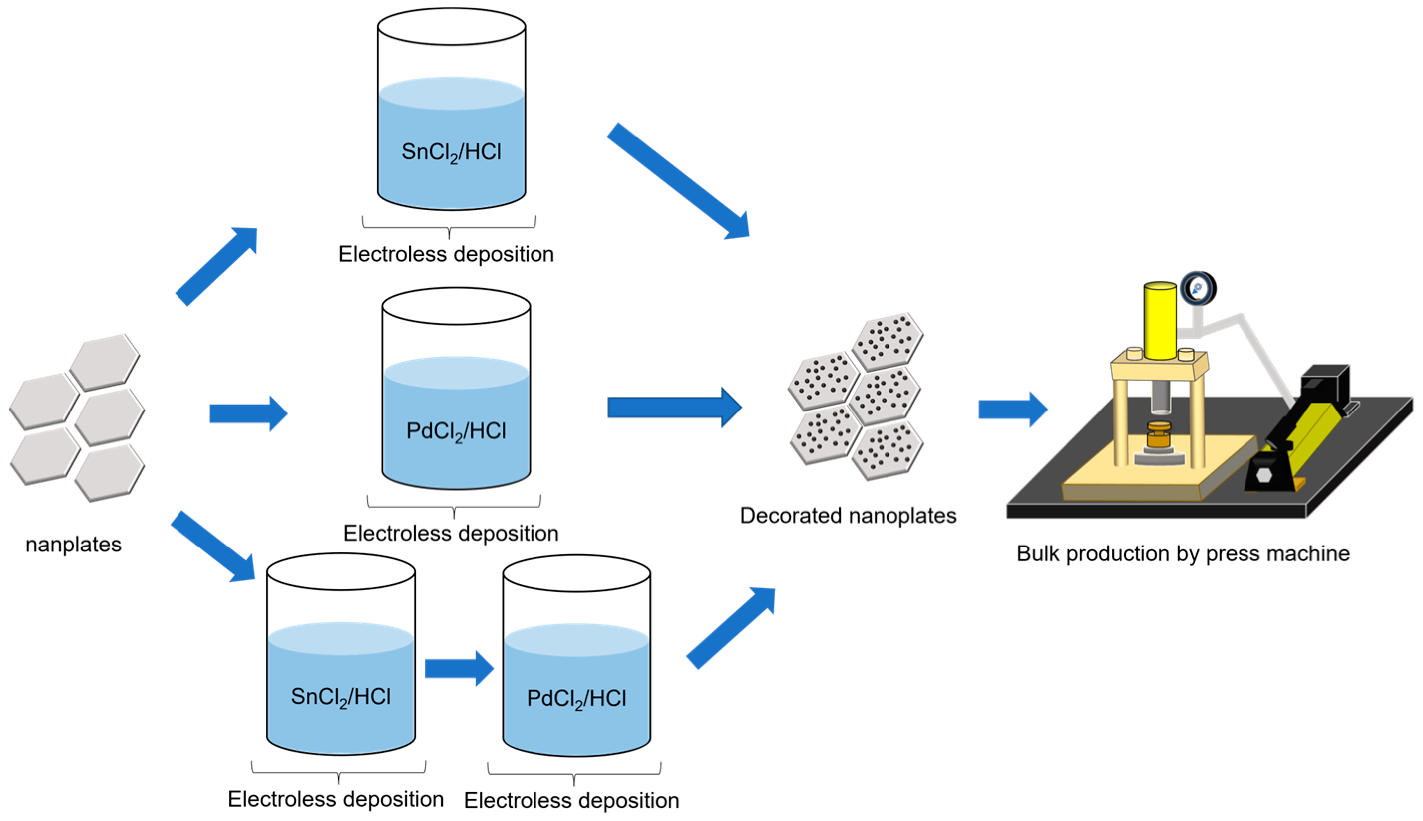
2. Materials and Methods

The studied Bi2Te3 nanoplates were fabricated via a solvothermal technique. The detailed fabrication procedure is described in previous studies [62,63,64]. In brief, Bi2Te3 nanoplates were fabricated as follows: 0.4 g of polyvinylpyrrolidone (PVP) (99.9% purity, K30, Ms ~40,000, Fujifilm Wako Co., Osaka, Japan) was dissolved in 18 mL of C2H6O2 (99.5% purity, Fujifilm Wako Co., Osaka, Japan). Subsequently, 20 mM of Bi2O3 (99.9% purity, Fujifilm Wako Co., Osaka, Japan), 70 mM of TeO2 (99.9% purity, Kojundo Chemical Lab., Sakado, Japan), and 2 mL of NaOH solution (0.5 M) (purity > 97.0%, Fujifilm Wako Co., Osaka, Japan) were added. The resultant solution was placed in an autoclave and heated to 200 °C for 4 h under continuous stirring. The precipitated products were collected using centrifugation and washed several times with distilled water and ethanol. The collected products were dried under vacuum at 60 °C for 24 h. The total weight of dried Bi2Te3 nanoplates was 0.71 g. The production efficiency, which is defined as the total weight of the dried Bi2Te3 nanoplates in the precursor solution divided by the weight of Bi and Te in the initial Bi2O3 and TeO2 powders, was 54%.
The process of metal deposition on the studied Bi2Te3 nanoplates is shown in Figure 1. A similar electroless deposition process has been described in our previous study [58]. To deposit the metals on the Bi2Te3 nanoplates, a displacement deposition method was used for electroless deposition [65]. Three types of metals were deposited on the Bi2Te3 nanoplates: Sn, Pd, and the lamination of Sn and Pd (Sn/Pd). For the Sn deposition, a precursor solution comprising 60 mM of SnCl2 (purity > 97.0%, Fujifilm Wako Co., Osaka, Japan) and 0.66 M of HCl (concentration of 35–37%, Fujifilm Wako Co., Osaka, Japan) was used. For the Pd deposition, a precursor solution comprising 1.1 mM of PdCl2 (purity > 99.0%, Fujifilm Wako Co., Osaka, Japan) and 0.66 M of HCl (concentration of 35–37%, Fujifilm Wako Co., Osaka, Japan) was used. The Bi2Te3 nanoplates (0.65 g) were immersed in each solution for 10 min. For the Sn/Pd deposition, the same conditions were used for the two solutions, as mentioned earlier. First, Bi2Te3 nanoplates (0.65 g) were immersed in the Sn-containing solution for 10 min. After rinsing with deionized water, the Sn-deposited Bi2Te3 nanoplates were immersed in the Pd-containing solution for 10 min. Thereafter, the three types of metal-deposited Bi2Te3 nanoplates were corrected using filter paper and rinsed with deionized water. In the end, the nanoplates were dried under vacuum at 60 °C for 24 h. In order to evaluate the thermoelectric properties of the prepared nanoplates by representing their properties as close as possible to those of pristine nanoplates, but not the melting structure, 0.38 g of nanoplates were pressed at approximately 300 K under uniaxial pressure (0.45 GPa). The samples were 22 mm long, 5 mm wide, and 0.6 mm thick.
The surface morphologies of the prepared nanoplates were examined using field-emission scanning electron microscopy (FE-SEM; S-4800, Hitachi, Tokyo, Japan), transmission electron microscopy (TEM; JEM-ARM200F, JEOL, Tokyo, Japan), and selected-area electron diffraction (SAED). The atomic composition of the nanoplates was determined using an electron probe microanalyzer (EPMA; EPMA-8050G, Shimadzu, Kyoto, Japan). The phase purity and crystal structure of the nanoplates were characterized using X-ray diffraction (XRD; MiniFlex 600, Rigaku, Tokyo, Japan) with Cu-Kα radiation (λ = 1.54 Å with 2θ ranging from 10° to 80°).
Thermal conductivity κ was calculated using the equation κ = αρC, where α, ρ, and C are thermal diffusivity, density, and specific heat, respectively. The thermal diffusivity α was measured at 300 K using a thermophysical-property-measuring instrument (Thermowave Analyzer, Bethel, Ishioka, Japan) based on spot-periodic heating radiation thermometry with an accuracy of ±5% [66]. This is a non-contact method that independently measures both in-plane and cross-plane thermal conductivity. Density was determined by measuring the size and mass. Literature values were used for the specific heat [14,67]. The electrical conductivity and Seebeck coefficient were measured at 300 K using the ZEM-3 method (Advance Riko, Yokohama, Japan) in a helium atmosphere with an accuracy of ±5%. Finally, the power factor and the dimensionless figure of merit were calculated.

3. Results and Discussion

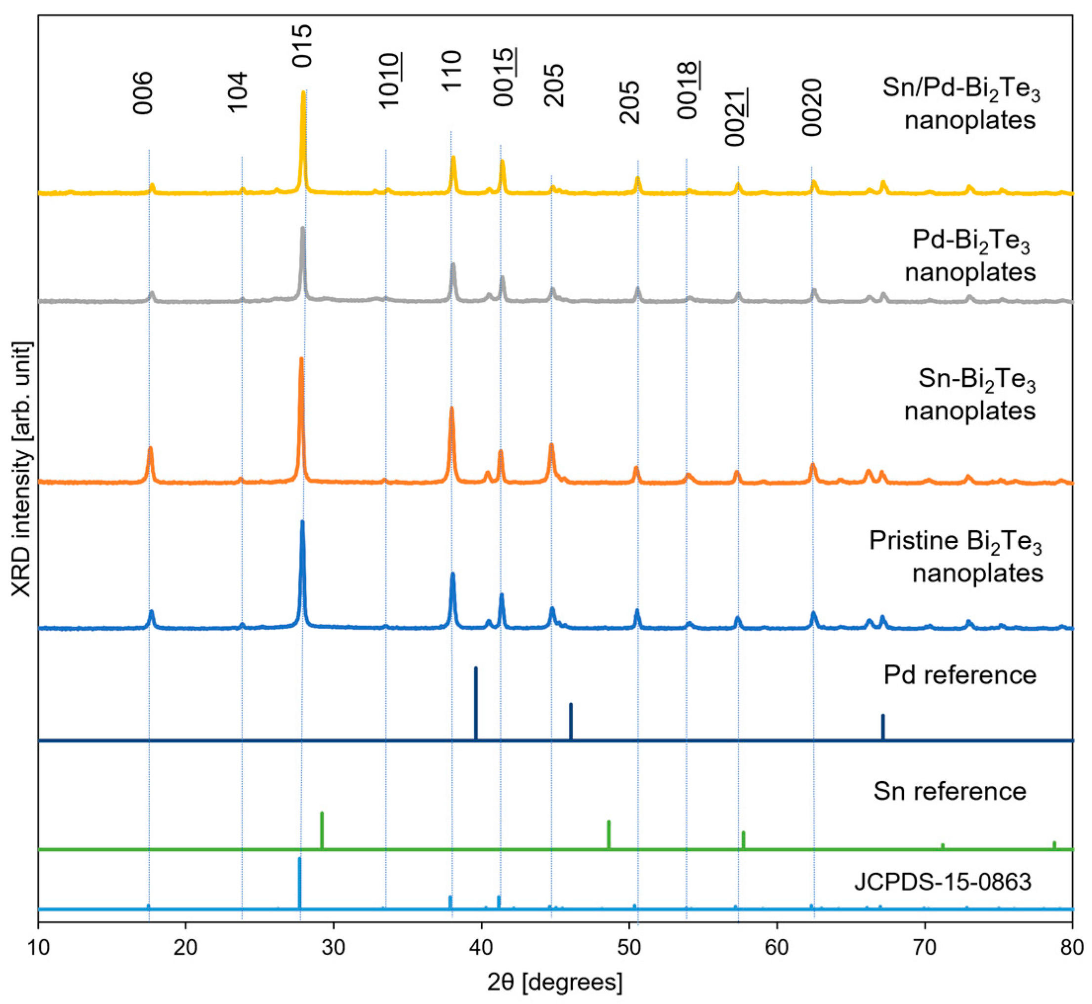
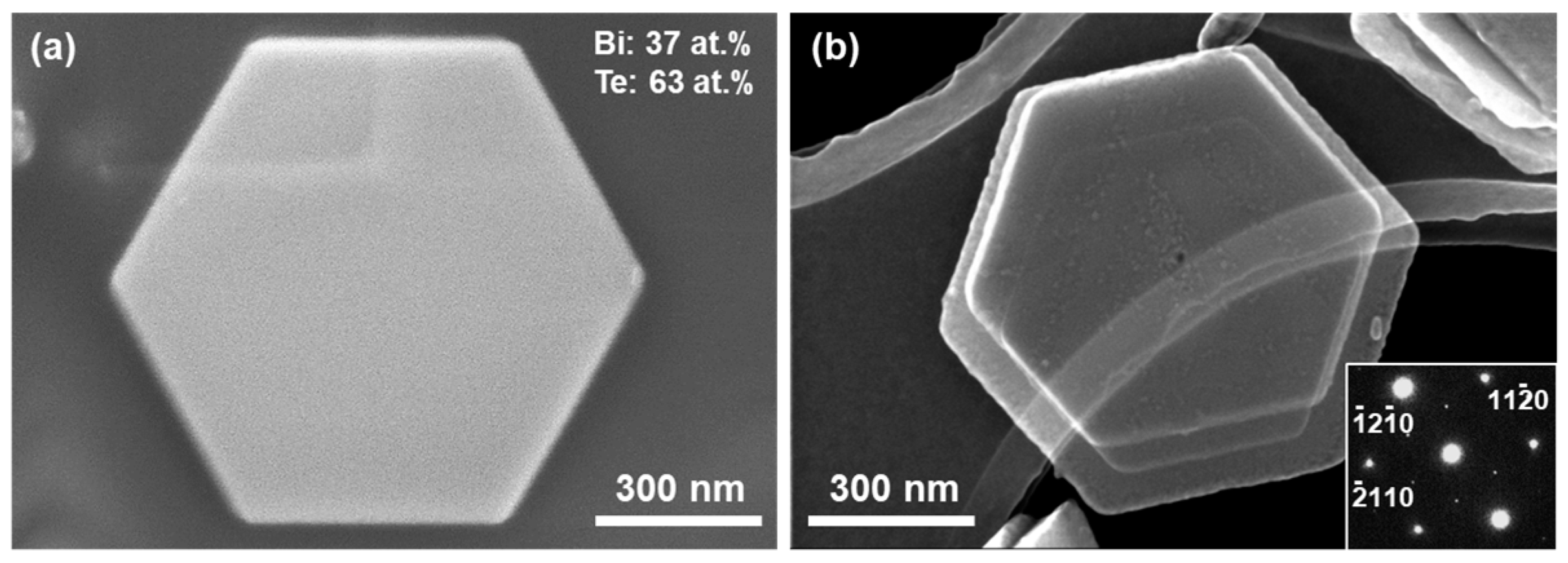
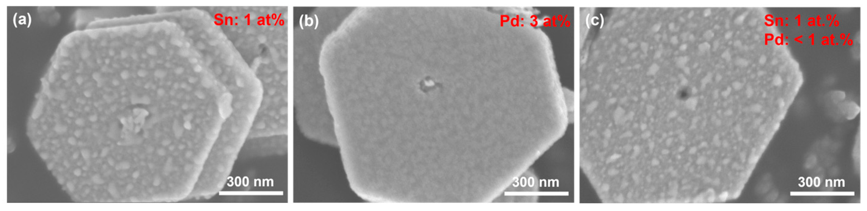
3.1. Structural Characteristics of Bi2Te3 Nanoplates Deposited with Different Metals

Figure 2 shows the structural characteristics of pristine Bi2Te3 nanoplates. The SEM image in Figure 2a shows that the Bi2Te3 nanoplates exhibited a significantly flat surface and a regular hexagonal shape with an approximate lateral size of 1 μm. The atomic composition of the plates (measured using EPMA) was 37 at% Bi and 63 at% Te, differing by 3% from the stoichiometric ratio (Bi:Te = 40:60). A TEM image of a typical Bi2Te3 nanoplate is shown in Figure 2b. The nanoplates were considerably thin (less than 50 nm) because of the overlap between the nanoplates and the mesh behind them. The SAED pattern shown in the inset of Figure 2b was indexed to the (00l) zone axis of rhombohedral Bi2Te3, which indicated that this nanoplate was single-crystalline. In brief, the mechanism of crystal growth of Bi2Te3 nanoplates is as follows [68]. After the chemical reactions, the Bi2Te3 nuclei were formed and subsequently aggregated. Bi2Te3 nanoparticles were generated when the radius of the aggregated nuclei exceeded their critical nucleus size. The nanoplate’s formation was attributed to its inherent crystal structure. Due to the high surface energy of the nuclei, the aggregated particles of Bi2Te3 were not in thermodynamic equilibrium and were metastable. As a result, Bi2Te3 nanoplates with better crystallinity became thermodynamically preferred. After Bi2Te3 nanoplates were formed, the Ostwald ripening process took place. The smaller nanoparticles adsorbed around the plates were consumed and grew gradually, leading to larger nanoplates along the top–bottom crystalline plane. This phenomenon happened because the rhombohedral Bi2Te3 can be described as a stack of infinite layers extending along the top–bottom crystalline plane connected by van der Waals bonds. From a thermodynamic perspective, the free energy of a broken covalent bond is higher than that of a dangling van der Waals bond. This suggests that Bi2Te3 crystal growth is faster along the top–bottom crystalline plane than along the c-axis, which is perpendicular to the top–bottom planes. This is because crystalline facets tend to develop on the low-index plane.
Figure 3 shows the SEM images of the Bi2Te3 nanoplates after electroless deposition of different metals. Notably, the SEM image of the Sn-Bi2Te3 nanoplates is referred to from our previous report [58]. As shown in Figure 3a, when Sn was deposited on the Bi2Te3 nanoplates, nanoparticles with a size of several tens of nanometers were dispersed on their surface. The concentration of Sn, as measured using EPMA, was 1 at%, suggesting that nanoparticle-shaped Sn was deposited on the prepared Bi2Te3 nanoplates. The surface morphology of the Pd-deposited Bi2Te3 nanoplates was different from that of the Sn-deposited nanoplates, as shown in Figure 3b. The nanoplate surface was covered with a thin, speckled Pd layer with a Pd concentration of 3 at%. Therefore, the shape and amount of deposition on the prepared Bi2Te3 nanoplates varied depending on the type of metal. This difference was attributed to the different liquid–solid interfacial free energies of Sn-Bi2Te3 and Pd-Bi2Te3 [59]. When the interfacial free energy was higher (as in the case of Sn-Bi2Te3), the crystals grew into island shapes. By contrast, when the interfacial free energy was lower (as in the case of Pd-Bi2Te3), the crystals grew in a layered shape. As shown in Figure 3c, when Sn and Pd were sequentially deposited on the nanoplate surface, the surface morphology was similar to that of the Sn-deposited nanoplates. The concentration of Sn was 1 at%, which was the same as for the Sn-deposited nanoplates; however, the concentration of Pd was less than 1 at%, which was lower than for the Pd-deposited nanoplates. These results suggest that Pd readily adhered to the Bi2Te3 surface but struggled to adhere to the Sn surface. The phase purity and crystal structure of the Bi2Te3 nanoplates with the electroless deposition of different metals were examined via XRD analysis, as shown in Figure 4. Bi2Te3 showed rhombohedral tetradymite-type crystal structures with the space group D 3 d 5 ( R 3 m ) and hexagonal unit cells. The lattice constant along the c-axis was 30.3 Å, while that along the a- or b-axis was 4.35 Å. The unit cell consists of five covalently bonded monatomic sheets arranged along the c-axis in the sequence –Te(1)–Bi–Te(2)–Bi–Te(1)–. The superscripts (1) and (2) indicate two distinct chemical states of the anions. The bonds between Te(1) and Bi include both covalent and ionic bonds, while Te(2) and Bi are purely covalently bonded. There is a very weak van der Waals attraction between adjacent Te(1) layers. Most of the peaks observed in the XRD patterns of the nanoplates without metal deposition were indexed to the standard diffraction pattern of Bi2Te3 (JCPDS 15-0863). The main peaks were observed in the c-axis-oriented (00l), (015), and (1010) planes, and several smaller peaks were also observed. Although electroless deposition was performed to deposit different metals on the nanoplate surface, the XRD patterns did not exhibit any peaks corresponding to those attributed to the deposited metals. This was due to the low crystallinity, i.e., extremely small crystallite size or high defect density, of the electrodeposited metals. Similar phenomena have been reported for the electrodeposited layers of bismuth-telluride-based alloys [58,69,70].

3.2. Thermal Conductivity of Bi2Te3 Nanoplates Deposited with Different Metals

Figure 5 shows the in-plane thermal conductivities of the bulk Bi2Te3 nanoplates with different metal depositions. The total thermal conductivity, κtotal, was estimated based on the measured thermal diffusivities, densities, and specific heats. The electronic thermal conductivity, κe, described in the inset was calculated from the experimentally measured electrical conductivities and using the Wiedemann–Franz law, given by κe = LσT. Here, the Lorenz number, L, was 2.44 × 10⁻⁸ WΩ/K2 for the classical free-electron model. The lattice thermal conductivity, κlattice, was obtained by subtracting the electronic thermal conductivity. The lattice thermal conductivities of all nanoplates were mostly the same as the total thermal conductivities, owing to their low electronic thermal conductivities, as shown in the inset. Notably, the thermal conductivities of the pristine Bi2Te3 nanoplates and the Sn-Bi2Te3 nanoplates are referred to from our previous report [58]. When electroless deposition was not performed on the Bi2Te3 nanoplates, the lattice thermal conductivity was 1.9 W/(m·K), corresponding to the lattice thermal conductivity of single-crystalline Bi2Te3 in the a- or b-axis directions (1.3–2.3 W/(m·K)) [71]. Following the metal deposition on the Bi2Te3 nanoplates, the lattice thermal conductivities decreased. In particular, the Sn-Bi2Te3 and Sn/Pd-Bi2Te3 nanoplates exhibited the lowest value of 1.1 W/(m·K), followed by the Sn/Pd-Bi2Te3 nanoplates with the value of 1.4 W/(m·K). This phenomenon indicates that the dispersion of metal nanoparticles on the nanoplate surface caused more phonons to scatter compared with a structure with a metal layer on the nanoplate surface, reducing the lattice thermal conductivity. This phenomenon was consistent with a previous report [72].

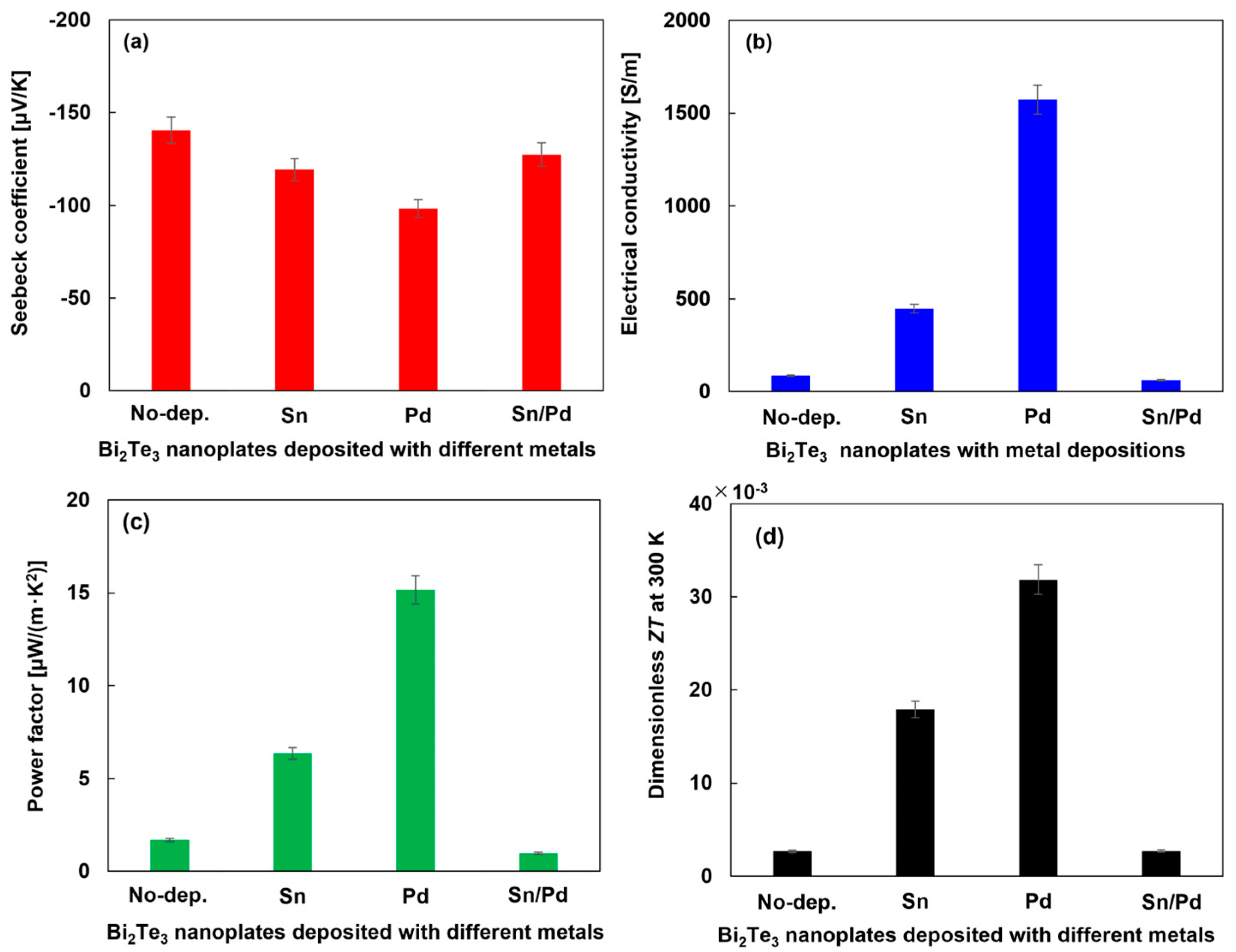
3.3. Thermoelectric Properties of Bi2Te3 Nanoplates Deposited with Different Metals

Figure 6 shows the in-plane thermoelectric properties of bulk-formed Bi2Te3 nanoplates deposited with different metals. In Figure 6a, the most negative Seebeck coefficient of −141 μV/K was observed in the Bi2Te3 nanoplates without metal deposition. The deposition of Sn and Pd on the Bi2Te3 nanoplates, respectively, decreased the negative Seebeck coefficient, which was strongly related to the carrier concentration. The relationship between the Seebeck coefficient S and carrier concentration n is given by Equation (1) [73,74], as follows:
S = 8 π 2 k B 2 T 3 e h 2 m * π 3 n 2 3 ,
where m* denotes effective mass. According to the above equation, the Seebeck coefficient scales inversely with the carrier concentration. Therefore, the negative Seebeck coefficient decreased because the carrier concentration corresponding to the metal concentration increased, owing to the metal deposition. In particular, the Pd-Bi2Te3 nanoplates exhibited the lowest negative Seebeck coefficient of −98 μV/K, owing to the high carrier concentration as determined by EPMA. By contrast, the Seebeck coefficient of the Sn/Pd-Bi2Te3 nanoplates negatively increased to −127 μV/K, corresponding to the value located between that for the Bi2Te3 nanoplates without metal deposition and that for the plates with Sn deposition. This was because the Sn/Pd-Bi2Te3 nanoplates had higher carrier concentrations compared to that of the Bi2Te3 nanoplates without metal deposition and lower carrier concentrations compared to that of Sn-Bi2Te3 and Pd-Bi2Te3 nanoplates. The mechanism for the lower carrier concentration when Sn and Pd were deposited simultaneously compared to when each was deposited alone is unclear. However, a possible explanation is that the carriers generated by the deposition of Sn and Pd could be offset by the coexistence of these two metals [75].
In Figure 6b, the electrical conductivity of the Bi2Te3 nanoplates without metal deposition is shown to be 86 S/m. The highest electrical conductivity of 1572 S/m was observed for the Pd-Bi2Te3 nanoplates, followed by 447 S/m for the Sn-Bi2Te3 nanoplates, owing to the increase in the carrier concentration compared to the Bi2Te3 nanoplates without metal deposition. By contrast, the Sn/Pd-Bi2Te3 nanoplates exhibited the lowest electrical conductivity of 60 S/m, which was lower than that of the pristine Bi2Te3 nanoplates. This phenomenon cannot be explained by the magnitude of the carrier concentration alone. Electrical conductivity σ is strongly related to the carrier concentration n as well as mobility μ, as expressed by Equation (2):
σ = n e μ .
Therefore, the Sn/Pd-Bi2Te3 nanoplates had a higher carrier concentration but lower mobility than the pristine Bi2Te3 nanoplates. The low mobility of Sn/Pd-Bi2Te3 nanoplates is due to electron scattering at the interfaces between the Sn and Pd layers.
The power factor of the Bi2Te3 nanoplates with different metal depositions is shown in Figure 6c. The power factor showed a trend similar to that of electrical conductivity because the inter-sample variation of the electrical conductivity was greater than the inter-sample variation of the Seebeck coefficient. The power factors of the Sn-Bi2Te3 and Pd-Bi2Te3 nanoplates were 6.4 and 15.2 μW/(m∙K2), respectively, which are higher than that of the pristine Bi2Te3 nanoplates at 1.7 μW/(m∙K2). Therefore, the power factor was improved by single-metal deposition on the nanoplatelets, and the power factor depended on the type of metals. However, the Sn/Pd-Bi2Te3 nanoplates exhibited the lowest power factor of 1.0 μW/(m∙K2), which was approximately 60% lower than that of pristine Bi2Te3 nanoplates, owing to the lowest electrical conductivity. Therefore, in this study, the simultaneous metal deposition did not enhance the power factor of the nanoplates.
The dimensionless ZT of the Bi2Te3 nanoplates with different metal depositions is shown in Figure 6d. The Pd-Bi2Te3 nanoplates exhibited the highest ZT of 32 × 10−3. This is because they had extremely high electrical conductivity among the four samples even though they did not have the lowest thermal conductivity or the highest negative Seebeck coefficient. The second highest ZT of 18 × 10−3 was exhibited by the Sn-Bi2Te3 nanoplates. Due to the lowest thermal conductivity of the Sn-Bi2Te3 nanoplates, the difference in ZT between the Pb-Bi2Te3 and Sn-Bi2Te3 nanoplates decreased compared to the difference in power factor between them. The ZT of the Sn/Pd-Bi2Te3 nanoplates was 2.7 × 10⁻³, which was the same value as the pristine Bi2Te3 nanoplates owing to the low thermal conductivity of the Sn/Pd-Bi2Te3 nanoplates. Therefore, all cases of the metal deposition on the Bi2Te3 nanoplates did not decrease the ZT. However, the highest ZT in this study was lower than that for the sintered Bi2Te3 bulk samples (ZT = 0.8 at 300 K) [76]. This was because the samples in this study underwent no sintering (e.g., spark plasma sintering) to assess the thermoelectric properties of the nanoplates by representing their properties as close as possible to those of the pristine nanoplates without melting. This study reveals the effects of different metal depositions on Bi2Te3 nanoplates, with implications regarding their thermoelectric performance. In addition, we consider there is room to improve thermoelectric performance by optimizing the type of metal and the amount of metal deposited. In the future, thermoelectric performance will be further improved by sintering nanoplates deposited with appropriate metals.

4. Conclusions

The studied Bi2Te3 nanoplates were deposited with Sn, Pd, and Sn/Pd, to modify their surface morphologies and improve their thermoelectric properties. The studied Bi2Te3 nanoplates were prepared using solvothermal techniques and metal deposition was performed using electroless deposition. Sn nanoparticles at a concentration of approximately 1 at% were deposited on the prepared Bi2Te3 nanoplates. For Pd deposition, a Pd layer with a concentration of approximately 3 at% was deposited on the Bi2Te3 nanoplates. When Sn and Pd were sequentially deposited on the nanoplate surface, the surface morphology was similar to that of the Sn-deposited nanoplates where the Sn and Pd concentrations were 1 at% and less than 1 at%, respectively. In order to assess the thermoelectric properties of the nanoplates by representing their properties as close as possible to those of the inherent nanoplate but not the melting structures, the nanoplate assemblies were compressed into thin bulk shapes at 300 K. The lattice thermal conductivity was affected by the surface morphology of the nanoplates. The Sn-Bi2Te3 and Sn/Pd-Bi2Te3 nanoplates exhibited the lowest value of 1.1 W/(m·K), indicating that the dispersion of metal nanoparticles on the nanoplate surface caused more phonon scattering. However, the Pd-Bi2Te3 nanoplates exhibited the highest power factor and dimensionless ZT owing to their significantly high electrical conductivities.

Author Contributions

K.K. (Kaito Kohashi) and M.T. conceived the study and designed the experiments. K.K. (Kaito Kohashi) and M.T. wrote the main manuscript. The experiments and data analysis were performed by Y.O., D.T. and K.K. (Keisuke Kaneko). Thermal analysis was performed by S.M. All authors discussed the results and commented on the manuscript. All authors have read and agreed to the published version of the manuscript.

Funding

This study was partially supported by the JSPS KAKENHI (grant number 22H04953).

Data Availability Statement

Research data can be shared by M.T. if requested.

Acknowledgments

The authors wish to thank Udono and Nishi at Ibaraki University and Tomita, Oguro, Yamazaki, and Sato at Tokai University for their support in conducting the experiments.

Conflicts of Interest

The authors declare no conflicts of interest.

References

  1. Landaluce, H.; Arjona, L.; Perallos, A.; Falcone, F.; Angulo, I.; Muralter, F. Review of IoT sensing applications and challenges using RFID and wireless sensor networks. Sensors 2020, 20, 2495. [Google Scholar] [CrossRef] [PubMed]
  2. Alsharif, M.H.; Kim, S.; Kuruoğlu, N. Energy harvesting techniques for wireless sensor networks/radio-frequency identification: A review. Symmetry 2019, 11, 865. [Google Scholar] [CrossRef]
  3. Guo, C.F.; Sun, T.; Cao, F.; Liu, Q.; Ren, Z. Metallic nanostructures for light trapping in energy-harvesting devices. Light Sci. Appl. 2014, 3, 161. [Google Scholar]
  4. Matiko, J.W.; Grabham, N.J.; Beeby, S.P.; Tudor, M.J. Review of the application of energy harvesting in buildings. Meas. Sci. Technol. 2014, 25, 012002. [Google Scholar] [CrossRef]
  5. Beeby, S.P.; Tudor, M.J.; White, N.M. Energy harvesting vibration sources for microsystems applications. Meas. Sci. Technol. 2006, 17, R175–R195. [Google Scholar] [CrossRef]
  6. Wei, C.; Jing, X. A comprehensive review on vibration energy harvesting: Modeling and realization. Renew. Sustain. Energy Rev. 2017, 74, 1–18. [Google Scholar] [CrossRef]
  7. Leonov, V. Thermoelectric energy harvesting of human body heat for wearable sensors. IEEE Sens. J. 2013, 13, 2284–2291. [Google Scholar] [CrossRef]
  8. Zhou, A.; Al-Furjan, M.S.H.; Zou, J.; Liu, W. A review on heat and mechanical energy harvesting from human—Principles, prototypes and perspectives. Renew. Sustain. Energy Rev. 2018, 82, 3582–3609. [Google Scholar] [CrossRef]
  9. Akinaga, H. Recent advances and future prospects in energy harvesting technologies. Jpn. J. Appl. Phys. 2020, 59, 110201. [Google Scholar] [CrossRef]
  10. Almoneef, T.S.; Erkmen, F.; Ramahi, O.M. Harvesting the energy of multi-polarized electromagnetic waves. Sci. Rep. 2017, 7, 14656. [Google Scholar] [CrossRef]
  11. Ioffe, A.F.; Stil’bans, L.S.; Iordanishvili, E.K.; Stavitskaya, T.S.; Gelbtuch, A.; Vineyard, G. Semiconductor thermoelements and thermoelectric cooling. Phys. Today 1959, 12, 42. [Google Scholar] [CrossRef]
  12. Champier, D. Thermoelectric generators: A review of applications. Energy Convers. Manag. 2017, 140, 167–181. [Google Scholar] [CrossRef]
  13. Zoui, M.A.; Bentouba, S.; Stocholm, J.G.; Bourouis, M. A Review on thermoelectric generators: Progress and applications. Energies 2020, 13, 3606. [Google Scholar] [CrossRef]
  14. Chiba, T.; Amma, Y.; Takashiri, M. Heat source free water floating carbon nanotube thermoelectric generators. Sci. Rep. 2021, 11, 14707. [Google Scholar] [CrossRef] [PubMed]
  15. Jaziri, N.; Boughamoura, A.; Müller, J.; Mezghani, B.; Fares, T.F.; Ismail, M. A comprehensive review of Thermoelectric Generators: Technologies and common applications. Energy Rep. 2020, 6, 264–287. [Google Scholar] [CrossRef]
  16. Zhang, L.; Lin, S.; Hua, T.; Huang, B.; Liu, S.; Tao, X. Fiber-based thermoelectric generators: Materials, device structures, fabrication, characterization, and applications. Adv. Enrrgy Mater. 2018, 8, 1700524. [Google Scholar] [CrossRef]
  17. Snyder, G.J.; Toberer, E.S. Complex thermoelectric materials. Nat. Mater. 2008, 7, 105–114. [Google Scholar] [CrossRef]
  18. Sootsman, J.R.; Chung, D.Y.; Kanatzidis, M.G. New and old concepts in thermoelectric materials. Angew. Chem. Int. Ed. 2009, 48, 8616–8639. [Google Scholar] [CrossRef]
  19. Chen, G.; Dresselhaus, M.S.; Dresselhaus, G.; Fleurial, J.-P.; Caillat, T. Recent developments in thermoelectric materials. Int. Mater. Rev. 2003, 48, 45–66. [Google Scholar] [CrossRef]
  20. Gomez-Romero, R. Hybrid organic–inorganic materials—In search of synergic activity. Adv. Mater. 2001, 13, 163–174. [Google Scholar] [CrossRef]
  21. Amma, Y.; Miura, K.; Nagata, S.; Nishi, T.; Miyake, S.; Miyazaki, K.; Takashiri, M. Ultra-long air-stability of n-type carbon nanotube films with low thermal conductivity and all-carbon thermoelectric generators. Sci. Rep. 2022, 12, 21603. [Google Scholar] [CrossRef]
  22. Judeinstein, P.; Sanchez, C. Hybrid organic–inorganic materials: A land of multidisciplinarity. J. Mater. Chem. 1996, 6, 511–525. [Google Scholar] [CrossRef]
  23. Van Bommel, K.J.C.; Friggeri, A.; Shinkai, S. Organic templates for the generation of inorganic materials. Angew. Chem. 2003, 42, 980–999. [Google Scholar] [CrossRef] [PubMed]
  24. Goldsmid, H.J. The electrical conductivity and thermoelectric power of bismuth telluride. Proc. Phys. Soc. 1958, 71, 633–646. [Google Scholar] [CrossRef]
  25. Soleimani, Z.; Zoras, S.; Ceranic, B.; Shahzad, S.; Cui, Y. A review on recent developments of thermoelectric materials for room-temperature applications. Sustain. Energy Technol. Assess. 2020, 37, 100604. [Google Scholar] [CrossRef]
  26. Yim, W.M.; Rosi, F.D. Compound tellurides and their alloys for Peltier cooling—A review. Solid-State Electron. 1972, 15, 1121–1134. [Google Scholar] [CrossRef]
  27. Peng, J.; Tikhonov, E. Predicted bismuth—Tellurium under high pressures. Phase Transit. 2023, 96, 328–336. [Google Scholar] [CrossRef]
  28. Masut, R.A.; André, C.; Vasilevskiy, D.; Turenne, S. Charge transport anisotropy in hot extruded bismuth telluride: Scattering by acoustic phonons. J. Appl. Phys. 2020, 128, 115106. [Google Scholar] [CrossRef]
  29. Zhang, W.; Liu, Z.; Tian, Z.; Zhang, Y.; Li, X.; Song, H. High thermoelectric performance of large size Bi2Te2.7Se0.3 alloy ingots. J. Electron. Mater. 2023, 52, 6682–6689. [Google Scholar] [CrossRef]
  30. Trung, N.H.; Sakamoto, K.; Toan, N.V.; Ono, T. Synthesis and evaluation of thick films of electrochemically deposited Bi2Te3 and Sb2Te3 thermoelectric materials. Materials 2017, 10, 154. [Google Scholar] [CrossRef]
  31. Goldsmid, H.J. Conversion Efficiency and Figure-of-Merit. In CRC Handbook of Thermoelectrics; Rowe, D.M., Ed.; CRC Press: New York, NY, USA, 1995; pp. 19–42. [Google Scholar]
  32. Hicks, L.D.; Dresselhaus, M.S. Effect of quantum-well structure on the thermoelectric figure of merit. Phys. Rev. B 1993, 47, 12727–12731. [Google Scholar] [CrossRef] [PubMed]
  33. Venkatasubramanian, R.; Siivola, E.; Colpitts, T.; O’Quinn, B. Thin-film thermoelectric devices with high room-temperature figures of merit. Nature 2001, 413, 597–602. [Google Scholar] [CrossRef]
  34. Peranio, N.; Eibl, O.; Nurnus, J. Structural and thermoelectric properties of epitaxially grown BiTe thin films and superlattices. J. Appl. Phys. 2006, 100, 114306. [Google Scholar] [CrossRef]
  35. Poudel, B.; Hao, Q.; Ma, Y.; Lan, Y.; Minnich, A.; Yu, B.; Yan, X.; Wang, D.; Muto, A.; Vashaee, D.; et al. High-thermoelectric performance of nanostructured bismuth antimony telluride bulk alloys. Science 2008, 320, 634–638. [Google Scholar] [CrossRef] [PubMed]
  36. Yu, F.; Zhang, J.; Yu, D.; He, J.; Liu, Z.; Xu, B.; Tian, Y. Enhanced thermoelectric figure of merit in nanocrystalline Bi2Te3 bulk. J. Appl. Phys. 2009, 105, 094303. [Google Scholar] [CrossRef]
  37. Kudo, S.; Hagino, H.; Takana, S.; Miyazaki, K.; Takashiri, M. Determining the thermal conductivities of nanocrystalline bismuth telluride thin films using the differential 3ω method while accounting for thermal contact resistance. J. Electron. Mater. 2015, 44, 2021–2025. [Google Scholar] [CrossRef]
  38. Boles, M.A.; Ling, D.; Hyeon, T.; Talapin, D.V. The surface science of nanocrystals. Nat. Mater. 2016, 15, 141–153. [Google Scholar] [CrossRef]
  39. Nakamoto, T.; Yokoyama, S.; Takamatsu, T.; Harata, K.; Motomiya, K.; Takahashi, H.; Miyazaki, Y.; Tohji, K. Aqueous chemical synthesis and consolidation of size-controlled Bi2Te3 nanoparticles for low-cost and high-performance thermoelectric materials. J. Electron. Mater. 2019, 48, 2700–2711. [Google Scholar] [CrossRef]
  40. Welch, C.M.; Compton, R.G. The use of nanoparticles in electroanalysis: A review. Anal. Bioanal. Chem. 2006, 384, 601–619. [Google Scholar] [CrossRef]
  41. Mody, V.V.; Siwale, R.; Singh, A.; Mody, H. Introduction to metallic nanoparticles. J. Pharm. Bioallied Sci. 2010, 2, 282–289. [Google Scholar] [CrossRef]
  42. Liu, J.L.; Wang, H.; Li, X.; Chen, H.; Zhang, Z.K.; Pan, W.W.; Luo, G.Q.; Yuan, C.L.; Ren, Y.L.; Lei, W. High performance visible photodetectors based on thin two-dimensional Bi2Te3 nanoplates. J. Alloys Compd. 2019, 798, 656–664. [Google Scholar] [CrossRef]
  43. Tiwari, J.; Tiwari, R.; Kim, K.S. Zero-dimensional, one-dimensional, two-dimensional and three-dimensional nanostructured materials for advanced electrochemical energy devices. Prog. Mater. Sci. 2012, 57, 724–803. [Google Scholar] [CrossRef]
  44. Wu, Z.; Mu, E.; Che, Z.; Liu, Y.; Sun, F.; Wang, X.; Hu, Z. Nanoporous (00l)-oriented Bi2Te3 nanoplate film for improved thermoelectric performance. J. Alloys Compd. 2020, 828, 154239. [Google Scholar] [CrossRef]
  45. Lu, W.; Ding, Y.; Chen, Y.; Wang, Z.L.; Fang, J. Bismuth telluride hexagonal nanoplatelets and their two-step epitaxial growth. J. Am. Chem. Soc. 2005, 127, 10112–10116. [Google Scholar] [CrossRef] [PubMed]
  46. Hollar, C.; Lin, Z.; Kongara, M.; Varghese, T.; Karthik, C.; Schimpf, J.; Eixenberger, J.; Davis, P.H.; Wu, Y.; Duan, X.; et al. High-performance flexible bismuth telluride thin film from solution processed colloidal nanoplates. Adv. Mater. Technol. 2020, 5, 2000600. [Google Scholar] [CrossRef] [PubMed]
  47. Mamur, H.; Bhuiyan, M.R.A.; Korkmaz, F.; Nil, M. A review on bismuth telluride (Bi2Te3) nanostructure for thermoelectric applications. Renew. Sustain. Energy Rev. 2018, 82, 4159–4169. [Google Scholar] [CrossRef]
  48. Ganesh, S.H.; Prabhu, A.N. A Review on doped/composite bismuth chalcogenide compounds for thermoelectric device applications: Various synthesis techniques and challenges. J. Electron. Mater. 2022, 51, 2014–2042. [Google Scholar]
  49. Hegde, G.S.; Prabhu, A.N.; Gao, Y.H.; Kuo, Y.K.; Reddy, V.R. Potential thermoelectric materials of indium and tellurium co-doped bismuth selenide single crystals grown by melt growth technique. J. Alloys Compd. 2021, 866, 158814. [Google Scholar] [CrossRef]
  50. Jin, Q.; Jiang, S.; Zhao, Y.; Wang, D.; Qiu, J.; Tang, D.-M.; Tan, J.; Sun, D.-M.; Hou, P.-X.; Chen, X.-Q.; et al. Flexible layer-structured Bi2Te3 thermoelectric on a carbon nanotube scaffold. Nat. Mater. 2018, 18, 62–68. [Google Scholar] [CrossRef]
  51. Chiba, T.; Yabuki, H.; Takashiri, M. High thermoelectric performance of flexible nanocomposite films based on Bi2Te3 nanoplates and carbon nanotubes selected using ultracentrifugation. Sci. Rep. 2023, 3, 3010. [Google Scholar] [CrossRef]
  52. Kango, S.; Klia, S.; Celli, A.; Njuguna, J.; Habibi, Y.; Kumar, R. Surface modification of inorganic nanoparticles for development of organic–inorganic nanocomposites—A review. Prog. Polym. Sci. 2013, 38, 1232–1261. [Google Scholar] [CrossRef]
  53. Li, F.; Song, J.; Yang, H.; Gan, S.; Zhang, Q.; Han, D.; Ivaska, A.; Niu, L. One-step synthesis of graphene/SnO2 nanocomposites and its application in electrochemical supercapacitors. Nanotechnology 2009, 20, 455602. [Google Scholar] [CrossRef] [PubMed]
  54. Kao, J.; Thorkelsson, K.; Bai, P.; Rancatore, B.; Xu, T. Toward functional nanocomposites: Taking the best of nanoparticles, polymers, and small molecules. Chem. Soc. Rev. 2013, 42, 2654–2678. [Google Scholar] [CrossRef] [PubMed]
  55. Lee, S.-S.; Jang, I.; Rhyee, J.-S.; Hong, S.-J.; Jong Yoo, S.; Park, I.K. Enhanced thermoelectric performance of Mo nanoparticle decorated n-type Bi2Te2.7Se0.3 powder composites. Appl. Surf. Sci. 2021, 548, 149200. [Google Scholar] [CrossRef]
  56. Min, Y.; Park, G.; Kim, B.; Giri, A.; Zeng, J.; Roh, J.W.; Kim, S.I.; Lee, K.H.; Jeong, U. Synthesis of multi-shell nanoplates by consecutive epitaxial growth of Bi2Se3 and Bi2Te3 nanoplates and enhanced thermoelectric properties. ACS Nano 2015, 9, 6843–6853. [Google Scholar] [CrossRef] [PubMed]
  57. Zheng, W.; Luo, Y.; Liu, Y.; Shi, J.; Xiong, R.; Wang, Z. Synergistical tuning interface barrier and phonon propagation in Au–Sb2Te3 nanoplate for boosting thermoelectric performance. J. Phys. Chem. Lett. 2019, 10, 4903–4909. [Google Scholar] [CrossRef] [PubMed]
  58. Kohashi, K.; Yamamoto, H.; Okano, Y.; Kaneko, K.; Miyake, S.; Takashiri, M. Low-dimensional heterostructures of tin nanoparticle-decorated Bi2Te3 nanoplates for reducing lattice thermal conductivity. Ceram. Int. 2024, 50, 764–771. [Google Scholar] [CrossRef]
  59. Chernov, A.A. Modern Crystallography III: Crystal Growth; Springer: Berlin, Germany, 1984; pp. 85–103. [Google Scholar]
  60. Cui, X.; Hutt, D.A.; Scurr, D.J.; Conway, P.P. The evolution of Pd∕Sn catalytic surfaces in electroless copper deposition. J. Electrochem. Soc. 2011, 158, D172. [Google Scholar] [CrossRef]
  61. Lin, W.P.; Wesolowski, D.E.; Lee, C.C. Barrier/bonding layers on bismuth telluride (Bi2Te3) for high temperature thermoelectric modules. J. Mater. Sci. Mater. Electron. 2011, 22, 1313–1320. [Google Scholar] [CrossRef]
  62. Takashiri, M.; Kai, S.; Wada, K.; Takasugi, S.; Tomita, K. Role of stirring assist during solvothermal synthesis for preparing single-crystal bismuth telluride hexagonal nanoplates. Mater. Chem. Phys. 2016, 173, 213–218. [Google Scholar] [CrossRef]
  63. Wada, K.; Tomita, K.; Takashiri, M. Fabrication of bismuth telluride nanoplates via solvothermal synthesis using different alkalis and nanoplate thin films by printing method. J. Cryst. Growth 2017, 468, 194–198. [Google Scholar] [CrossRef]
  64. Yamazaki, H.; Eguchi, R.; Takashiri, M. Investigation of phase transition from critical nucleus to Bi2Te3 nanoplate based on screw dislocation-driven spiral growth by solvothermal synthesis. Cryst. Res. Technol. 2021, 56, 2100153. [Google Scholar] [CrossRef]
  65. Yae, S.; Nasu, N.; Matsumoto, K.; Hagihara, T.; Fukumuro, N.; Matsuda, H. Nucleation behavior in electroless displacement deposition of metals on silicon from hydrofluoric acid solutions. Electrochim. Acta 2007, 53, 35–41. [Google Scholar] [CrossRef]
  66. Nagata, S.; Nishi, T.; Miyake, S.; Azuma, N.; Hatori, K.; Awano, T.; Ohta, H. Development of novel thermal diffusivity analysis by spot periodic heating and infrared radiation thermometer method. Materials 2020, 13, 4848. [Google Scholar] [CrossRef] [PubMed]
  67. Parker, W.J.; Jenkins, R.J.; Butler, C.P.; Abbott, G.L. Flash method of determining thermal diffusivity, heat capacity, and thermal conductivity. J. Appl. Phys. 1961, 32, 1679–1684. [Google Scholar] [CrossRef]
  68. Takashiri, M. Thin Films of Bismuth-Telluride-Based Alloys. In Thermoelectric Thin Films; Mele, P., Narducci, D., Ohta, M., Biswas, K., Morante, J., Saini, S., Endo, T., Eds.; Springer: Cham, Switzerland, 2019; pp. 1–30. [Google Scholar]
  69. Hatsuta, N.; Takemori, D.; Takashiri, M. Effect of thermal annealing on the structural and thermoelectric properties of electrodeposited antimony telluride thin films. J. Alloys Compd. 2016, 685, 147–152. [Google Scholar] [CrossRef]
  70. Yamauchi, K.; Mori, R.; Yamaguchi, M.; Takashiri, M. Thermoelectric properties including thermal conductivity of electrodeposited bismuth selenide thin films fabricated using different acid solutions. J. Alloys Compd. 2019, 792, 222–229. [Google Scholar] [CrossRef]
  71. Al-Alam, P.; Pernot, G.; Isaiev, M.; Lacroix, D.; Vos, M.D.; Stein, N.; Osenberg, D.; Philippe, L. Lattice thermal conductivity of Bi2Te3 and SnSe using Debye-Callaway and Monte Carlo phonon transport modeling: Application to nanofilms and nanowires. Phys. Rev. B 2019, 100, 115304. [Google Scholar] [CrossRef]
  72. He, S.; Lehmann, S.; Bahrami, A.; Nielsch, K. Current state-of-the-art in the interface/surface modification of thermoelectric materials. Adv. Energy Mater. 2021, 11, 2101877. [Google Scholar] [CrossRef]
  73. Singkaselit, K.; Sakulkalavek, A.; Sakdanuphab, R. Effects of annealing temperature on the structural, mechanical and electrical properties of flexible bismuth telluride thin films prepared by high pressure RF magnetron sputtering. Adv. Nat. Sci. Nanosci. Nanotechnol. 2017, 8, 035002. [Google Scholar] [CrossRef]
  74. Lee, K.H.; Kim, S.-I.; Lim, J.-C.; Cho, J.Y.; Yang, H.; Kim, H.-S. Approach to determine the density-of-states effective mass with carrier concentration-dependent Seebeck coefficient. Adv. Funct. Mater. 2022, 32, 2203852. [Google Scholar] [CrossRef]
  75. Deng, Y.; Zhou, X.-S.; Nan, C.-W. Solvothermal preparation and thermoelectric properties of ternary Sn–Bi–Te alloy. Phys. Status Solidi A 2003, 199, 265–271. [Google Scholar] [CrossRef]
  76. Yu, F.; Xu, B.; Zhang, J.; Yu, D.; He, J.; Liu, Z.; Tian, Y. Structural and thermoelectric characterizations of high pressure sintered nanocrystalline Bi2Te3 bulks. Mater. Res. Bull. 2012, 47, 1432–1437. [Google Scholar] [CrossRef]
Figure 1. Schematic of fabrication processes for metal deposition on Bi2Te3 nanoplates, followed by compression into thin bulk shapes.
Crystals 14 00132 g001
Figure 2. (a) SEM image of a Bi2Te3 nanoplate with atomic composition determined by EPMA and (b) TEM image of a Bi2Te3 nanoplate and the corresponding SAED pattern.
Crystals 14 00132 g002
Figure 3. SEM images of Bi2Te3 nanoplates fabricated using electroless deposition with (a) Sn [58], (b) Pd, and (c) Sn/Pd.
Crystals 14 00132 g003
Figure 4. X-ray diffraction patterns of Bi2Te3 nanoplates deposited with different metals using electroless deposition.
Crystals 14 00132 g004
Figure 5. In-plane thermal conductivities of bulk-formed Bi2Te3 nanoplates deposited with different metals using electroless deposition measured at 300 K. The inset describes the electronic thermal conductivity of the nanoplates determined using the Wiedemann–Franz law.
Crystals 14 00132 g005
Figure 6. In-plane thermoelectric properties of bulk-formed Bi2Te3 nanoplates deposited with different metals using electroless deposition measured at 300 K. (a) Seebeck coefficient, (b) electrical conductivity, (c) power factor, and (d) dimensionless figure of merit.
Crystals 14 00132 g006
Disclaimer/Publisher’s Note: The statements, opinions and data contained in all publications are solely those of the individual author(s) and contributor(s) and not of MDPI and/or the editor(s). MDPI and/or the editor(s) disclaim responsibility for any injury to people or property resulting from any ideas, methods, instructions or products referred to in the content.

