Article

Microstructure Effects on Anodizing High-Silicon Aluminium Alloy AlSi12Cu1(Fe) under Various Surface Conditions and Power Modes

by
Emel Razzouk
1,
Dániel Koncz-Horváth
2 and
Tamás I. Török
1,*
1
Institute of Chemical Metallurgy and Foundry Engineering, University of Miskolc, 3515 Miskolc, Hungary
2
Institute of Physical Metallurgy, Metal Forming and Nanotechnology, University of Miskolc, 3515 Miskolc, Hungary
*
Author to whom correspondence should be addressed.
Crystals 2024, 14(4), 352; https://doi.org/10.3390/cryst14040352
Submission received: 19 March 2024 / Revised: 5 April 2024 / Accepted: 7 April 2024 / Published: 9 April 2024
(This article belongs to the Special Issue Metal Oxide Thin Films, Nanomaterials and Nanostructures)

Abstract

:
This study investigates the impact of the surface characteristics and the inner close-to-surface characteristics of die-cast Al-Si-Cu alloy on the anodizing process under steady-state voltage and current modes. Samples of industrial-pressure die-cast aluminium–silicon alloy AlSi12Cu1(Fe) underwent anodization in as-die-cast surface conditions and after surface-grinding operations with material removal of 0.1, 0.5, and 1 mm. After surface grinding operations, the anodic layer thickness was significantly greater when subjected to a steady-state voltage of 35 V compared to that formed under a steady-state voltage of 20 V, showing an increase in the range of 2 to 2.5 times more than the thickness at 20 V. Additionally, anodizing under steady-state current mode (1.6 A·dm−2) yielded thicker layers compared to steady-state voltage mode (35 V, 1.6 A·dm−2 max) across all surface states (as-cast, ground). SEM-EDS analysis with element mapping revealed the subsequent effects of element distribution on anodic layer growth and structure. Grinding prior to anodization resulted in larger cavity sizes and lengths, attributed to microstructural variations induced by grinding. Grinding also exposed areas with slower solidification rates, fostering a homogeneous Al phase that facilitated enhanced oxide growth. Moreover, the formation of oxide was directly correlated with the presence of alloying elements, particularly silicon particles, which influenced the presence of the unanodized aluminium regions.

1. Introduction

Die casting is a flexible method used to create complex metal components. This method involves feeding the liquefied metal into durable steel molds, referred to as dies, under considerable pressure. The designed dies can have intricate forms while maintaining precise and consistent results. This process yields finely structured parts with relatively smooth surfaces, even in exterior areas, making them suitable for applying appealing and functional coatings afterward [1].
During anodizing, the primary elementary component that dissolves during such an electrochemical surface treatment is the base metal, i.e., the aluminium; in principle, all aluminium alloys can be surface-oxidized by this process. However, practical knowledge suggests that the anodization process of the substrate is affected by the presence of certain alloying elements, and the level of difficulty rises when the alloy contains high amounts of them. Taking this into account, it is intriguing to observe that cast alloys are considerably more difficult to anodize than wrought alloy of good quality [2,3].
Nevertheless, the cast-type Al-Si alloys, due to their favorable characteristics such as excellent castability, low shrinkage, and high specific strength [4,5], are still widely utilized in the production of mechanical components, which occasionally have anodized surface finish as well. In recent times, certain eutectic or near-eutectic Al-Si alloys like AlSi12 and AlSi10Mg have emerged as highly promising materials for additive manufacturing of Al alloy products [6,7]. However, the relatively low hardness and inadequate corrosion and abrasion resistance properties impose significant limitations on the durability of such Al-Si alloy products [8,9]. Consequently, various surface technologies, including anodizing [10], laser remelting [11], plasma electrolytic oxidation (PEO) [12], and cathode plasma electrolytic deposition [13], have been employed to address these concerns.
The oxide film produced by anodizing is composed of two distinct layers: a thin, nonporous dielectric base layer in direct contact with the underlying metal, known as the barrier layer, and a porous surface layer situated above it [14,15,16,17]. The barrier layer plays a crucial role in enhancing the overall anticorrosion properties, while the outer porous structure renders the film susceptible to corrosion in aggressive environments due to its high absorbency. To mitigate this vulnerability, anodized films commonly receive an additional physical or chemical sealing treatment, effectively reducing the porosity and adsorption capacity of the oxide layer [18].
Cast Al-Si alloys exhibit a bimodal microstructure, characterized by α -Al dendrites and a eutectic alpha-Al + Si aggregate [19,20]. Among the various Al-Si foundry alloys, the anodizing response of hypoeutectic alloys (Si content < 12.6 wt%) has been extensively studied. The microstructure of these alloys comprises an α –Al primary phase and a eutectic mixture of silicon and aluminium. Depending on the chemical composition of the alloy and cooling rate during solidification, intermetallic compounds may also be present in the interdendritic regions and along the grain boundaries. In Al-Si alloys, the growth of the anodic layer is primarily impeded by the presence of Si particles and intermetallic compounds rich in Cu, Mg, and Fe. These elements not only diminish the surface mechanical properties of the oxide layer but also lead to the formation of aesthetic defects on the anodized surface of the castings [21,22]. The chemical composition and microstructure of the substrate have a significant impact on the growth and final characteristics of the oxide layer during anodization [23]. The anodizing process of cast Al alloys results in oxidized surfaces with a lower quality due to high amounts of Si and other elements, especially those of Fe and Cu [24]. The presence of alloying elements in solid solution typically does not have a significant effect on the anodizing response of Al alloys. However, the formation of precipitates or intermetallic particles within the α –Al matrix or along grain boundaries can compromise the integrity of the oxide layer [25]. These compounds often have different oxidation rates compared to pure Al due to their positions in the so-called electrochemical series or standard redox potentials of elements [26]. Intermetallic phases with more positive redox standard potentials (i.e., being more noble) than the α –Al matrix exhibit slower oxidation rates and remain there as unanodized particles at the end of the anodizing process. Conversely, intermetallic compounds with higher oxidation energies are completely dissolved during anodization, resulting in the formation of excess porosities within the oxide layer [2].
Oxide layer growth during anodizing is significantly affected by the chemical composition of the electrolyte. When the products of the anodic reaction are insoluble in the electrolyte, a strongly adherent barrier-type film is formed. As a result, at relatively high voltage levels, a thin and dielectric compact film is produced when using neutral pH salt solutions like borate or tartrate electrolytes [27]. On the other hand, when working with acidic electrolytes such as sulfuric, phosphoric, chromic, and oxalic acids, a porous oxide layer is formed on top of the barrier layer. The solubility of the reaction products in these acidic electrolytes leads to the creation of a more porous outer structure in the oxide layer during anodizing [27]. This difference in the characteristics of the oxide layer formed under different electrolyte conditions has important implications for the surface properties and applications of anodized Al-Si alloys [26].
The development of the oxide layer is also associated with the casting technique employed. Labisz et al. conducted a study [28] comparing the anodizing process of Al-Si-based alloys manufactured through pressure die casting and sand casting. The results revealed that the anodized layer is thicker in the case of sand-cast materials compared to those produced by pressure die casting. In a separate investigation by Ridder et al. [29], anodized Al surfaces from four different fabrication methods (namely, extruding, permanent mold casting, sand casting, and high-pressure die casting (HPDC)) were examined. The study indicated that the uniformity of the oxide layer on an extruded sample could be attributed to the low Si content of the alloy as well as the fabrication method. Conversely, materials produced by casting processes displayed non-uniform-thickness oxide layers on the surface, with the HPDC sample exhibiting the lowest mean value and the greatest scattering due to the high cooling rate associated with the HPDC process.
The present study investigates the chemical element distribution in the anodic layer when the anodizing process is accomplished in as-die-cast condition and after surface-grinding operations. All the laboratory experiments were carried out under the same treatment sequence and utilizing identical anodizing parameters. We aimed to gain a deeper understanding of how the alloy’s microstructure influences the properties of the anodic layer formed during the anodizing process.

2. Materials and Methods

2.1. Materials

A set of AlSi12Cu1(Fe) die-cast alloy samples (Al 84.4; Si 12.6; Fe 1.07; Mg 1.05; Cu 0.85, all in wt.% analyzed by EDS) were subjected to testing. The tested samples were cut from the original cast product as small specimens with a total surface area of 20 cm2. The samples possessed flat surfaces that underwent polishing to remove varying amounts of material (0.1, 0.5, and 1 mm). The grinding technique involved monitoring the thickness using a caliper measuring tool both before and during the grinding process to attain the desired final sample thickness. The wet grinding process was carried out using SiC abrasive paper in order to keep the surface roughness close to the as-cast surface roughness Ra = 0.72 µm and Rz = 4.7 µm. The samples were affixed to a holder positioned between two cathodes, situated at a distance of 7 cm. The sample numbers employed in the experiments are detailed in Table 1.
To achieve the requisite current density in the anodizing process, numerous attempts were undertaken. Ultimately, two voltage values were applied: 20 V and 35 V. The voltage increased gradually to attain the desired voltage in steady-state voltage (SSV) mode. Subsequently, by transitioning to steady-state current (SSC) mode, the minimum current density achieved in the steady-state voltage mode (35 V) was maintained.

2.2. Anodizing Process

The anodizing process consists of three steps: pretreatment, anodizing (oxide layer growth), and post-treatment. In this research, we excluded the post-treatment step in order to reveal the effect of anodizing parameters on the anodic layer thickness and structure.
The first stage in the pretreatment step is the degreasing process. Degreasing is a vital preprocessing step aimed at achieving optimal wetting characteristics, thereby promoting uniformity in subsequent processing steps on the substrate surface [30], because the as-cast alloys of this type often have grease and oils on their surfaces. In our experiments, the degreasing solution used contained phosphates, borates, and potassium hydroxide and were moderately alkaline and free of silicon compounds. The samples were immersed in this degreasing solution using an ultrasonic cleaning device for 10 min at 65 °C. After degreasing, the samples were rinsed in distilled water. The last stage in the pretreatment was pickling, when the samples were immersed in the pickling solution containing 181.4 g·L−1 sulfuric acid, 8.1 g·L−1 Al, and 7 g·L−1 hydrogen peroxide for 15 s. After pretreatment, the samples were fixed to the anode, which was made from titanium, and placed in the desired position using an anode holder. The cathode as well was made from titanium and connected to the negative pole of the power supply unit. The purpose of using titanium is due to its strong stability in the electrolyte medium which contains sulfuric acid and oxalic acid. The pump and refrigerator were used to adjust the electrolyte temperature to the desired temperature for the anodizing process; this step is the first step before starting the anodizing process, and this step was accomplished by using a thermometer and recording the electrolyte temperature inside the container, which was made of double-wall glass.
Anodic layers were fabricated in the electrolyte medium containing 181.1 g·L−1 sulfuric acid, 10.6 g·L−1 Al, and 7.1 g·L−1 oxalic acid as well. The current was provided by a DC power supply unit (QPX600 Dual 600Watt). The electrolyte was in continuous agitation and maintained at a temperature of 18 °C.

2.3. Examination Methods Analytical Techniques

The microstructure and the anodic layer thickness were examined using scanning electron microscopy (Thermo Fischer Helios G4 PFIB SEM, Thermo Fischer, Waltham, MA, USA), and the chemical composition of the sample cross section was identified using energy-dispersive X-ray spectroscopy (EDS).

3. Results and Discussion

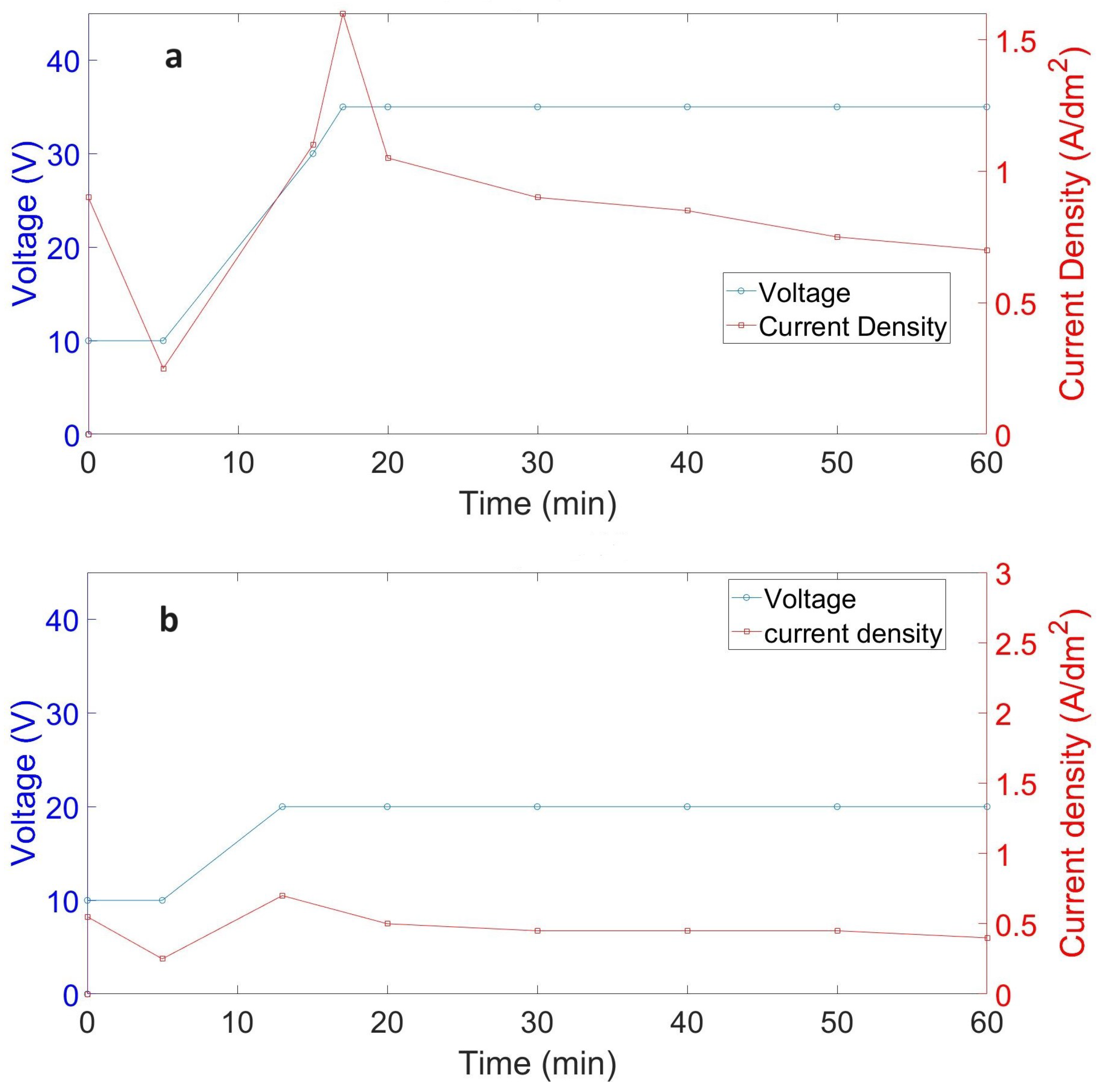
3.1. Voltage–Current Density Behavior

By tracking changes in current density in SSV and SSC modes, one could anticipate the behavior of anodic layer growth. In the SSV mode, after reaching the desired steady voltage in both cases (20 and 35 V), the current density began to decrease incrementally, as shown in Figure 1. This decrease was more pronounced at 35 V than at 20 V. The reduction in current density over the 60 min anodizing process indicates a change in resistance, signifying a shift in the anodic layer thickness. Regarding SSC, Figure 2 depicts that after reaching the desired current of 1.6 A·dm−2, the voltage continued to increase throughout the anodizing duration. As the anodic layer constitutes an insulating oxide, the rise in voltage corresponds to an increase in the anodic layer thickness.

3.2. The Anodic Layer Thicknesses

The scanning electron microscopy (SEM) technique was utilized for the measurement of the anodic layer thickness. Many measurements of the anodic layer thickness were conducted at various points. This was undertaken due to the heterogeneous microstructure of the alloy and the potential defects present in the casting alloy, as illustrated in Figure 3.
For the as-cast surface, by applying a SSV of 35 V, it is associated with a maximum current density of 1.6 A·dm−2, which is higher than that corresponding to 20 V. In this scenario, the total anodic layer developed after 60 min in the SSV was greater at 35 V compared to the 20 V, as illustrated in Figure 4. This difference in thickness may be associated with the enhancement of other properties, such as corrosion and wear resistance. Notably, this difference represents a change in the thickness of approximately 12%. This alteration in thickness holds significance in the context of cast Al-Si alloy, given the challenges associated with anodizing this type of alloy and the presence of the silicon and others element such as copper and iron.
The anodizing power mode also plays a crucial role in determining the anodizing thickness, as demonstrated in Figure 4. The mode transition to SSC, while maintaining the current density 1.6 A·dm−2, results in a higher anodic layer thickness compared to the anodic layer thickness produced in SSV for the as-cast surface, as depicted in Figure 4. Specifically, the anodic layer thickness increases by 2.8 times compared to SSV (20 V) and 2.5 times compared to SSV (35 V). The total charge received during the anodizing process for these three samples appears in Table 1; as the anodizing process depends on the current density and the anodizing duration, we can expect the higher anodic layer thickness produced in the sample CC1 in SSC mode. As observed in Figure 3, the surface layer may contain defects associated with the casting process and chemical composition. In the case of the Al-Si cast alloy, the cooling rate significantly influences the microstructure of the surface region, which has a higher cooling rate than the bulk material. To investigate the impact of the skin layer on the behavior and growth of the anodic layer, some samples underwent grinding to remove varying material depths (0.1, 0.5, and 1 mm). Subsequently, an SSV (20 and 35 V) was applied in the anodizing process, and some samples underwent SSC (1.6 A·dm−2). Figure 4 illustrates the anodic layer thickness across all scenarios.
For both applied voltages (20 V and 35 V), the anodic layer thickness increased with greater material removal through grinding. Notably, the anodic layer thickness generated at 35 V was significantly higher than that produced at 20 V, showing an increase in the range of 2 to 2.5 times compared to the thickness achieved at 20 V. The data in Table 1 clearly show a link between the total applied charge (apparent charge) to the samples and the thickness of the anodic layer. In both SSV conditions, a consistent rise in charge was observed when material was incrementally removed from the surface. This divergence stems from disparities in surface roughness and the composition of the alloy. These differences in surface characteristics contribute significantly to the observed variations in the charge accumulation during the process, underscoring the impact of surface condition on the overall electrochemical behavior. Different surface states could need different amounts of activation energy or starting charge to start the anodizing process; this is especially noticeable when comparing polished and as-cast surfaces.

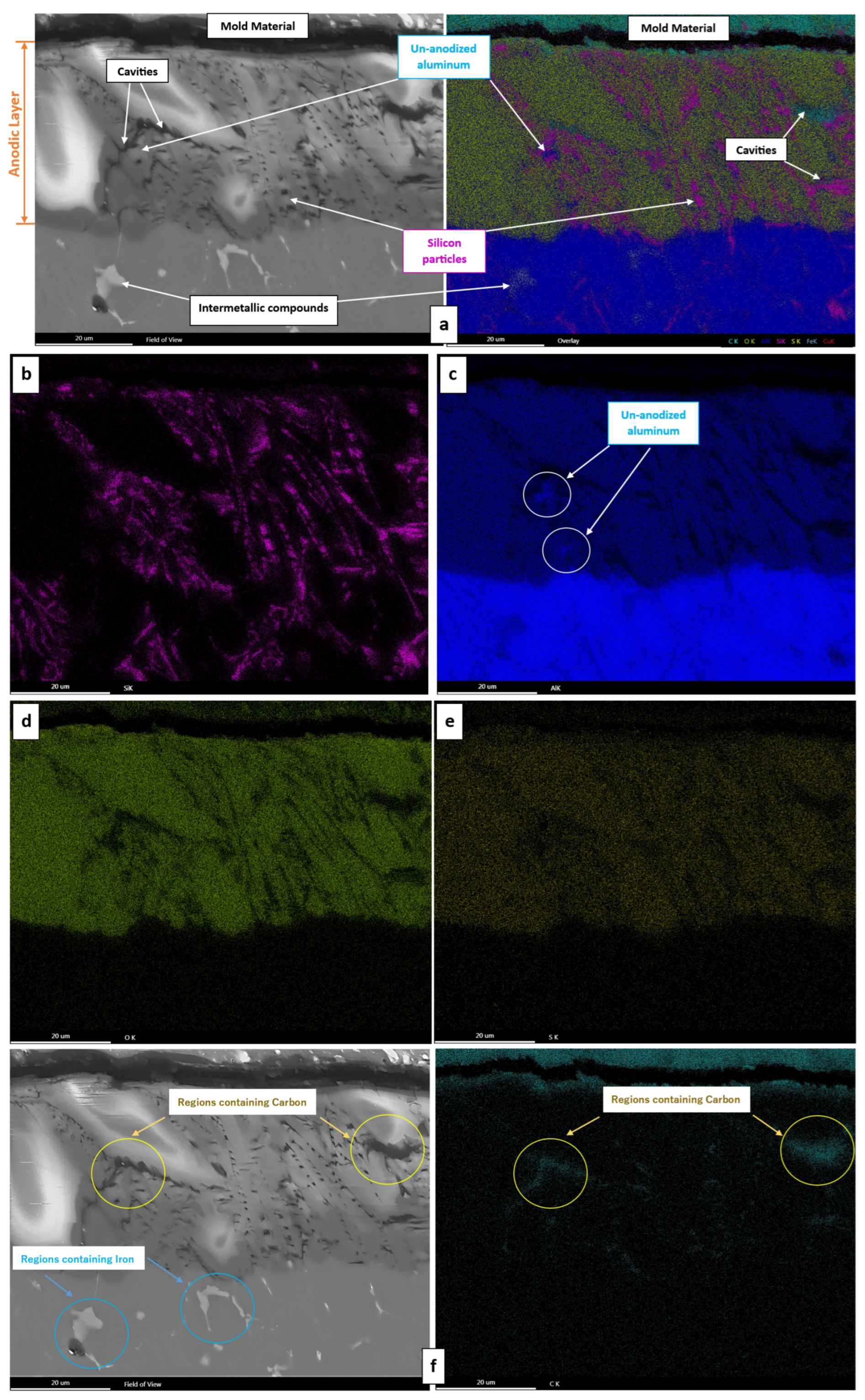
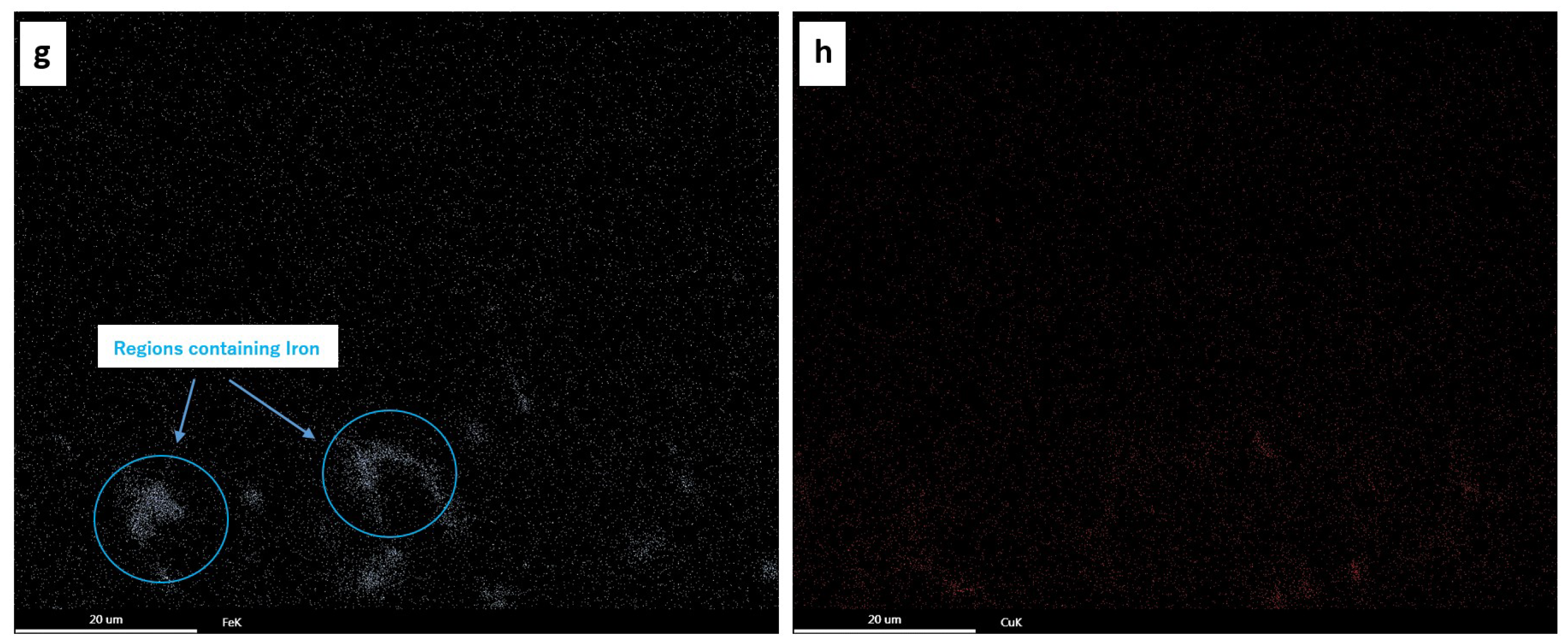
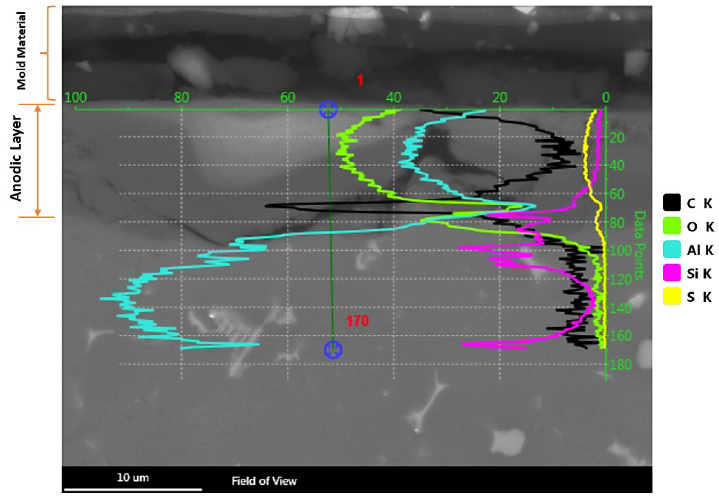
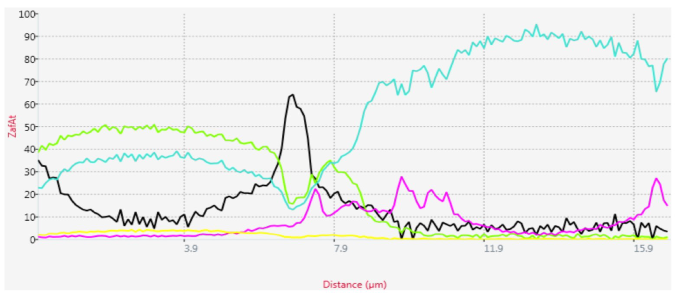
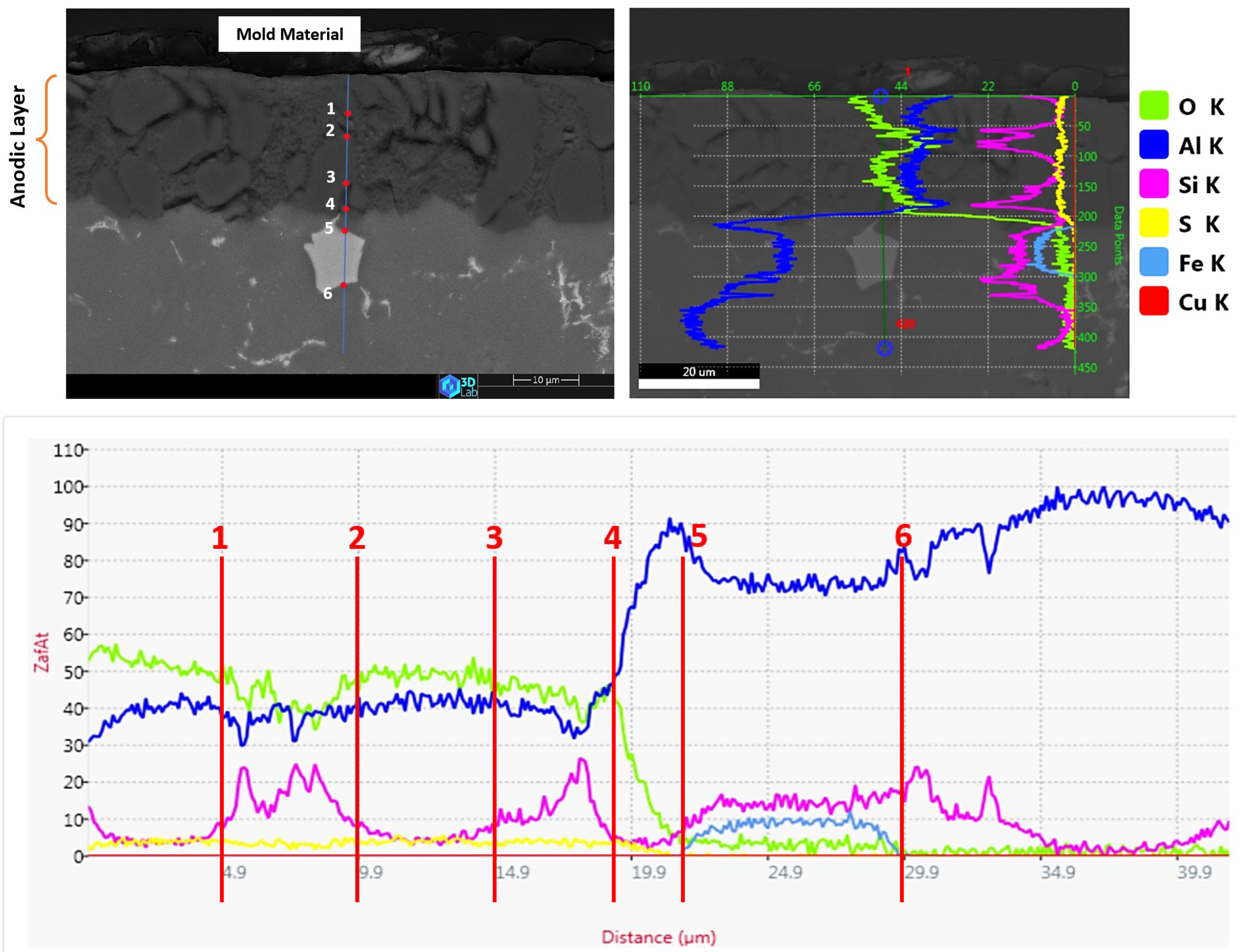
3.3. The Anodic Layer Composition

The alloy shown in Figure 5 has a heterogeneous microstructure consisting of intermetallic, eutectic, and aluminium compounds. These microstructural differences cause the anodic layer growth rate to change. Furthermore, Figure 5 illustrates the variations in structural phase sizes in comparison to the bulk material. Thus, the removal of the surface region that has a finer structure is responsible for the observed rise in the anodic thickness. This phenomenon arises from rapid solidification compared to the bulk alloy.
As shown in Figure 6, the examination of the element distribution in the cross sections of the base alloy and the anodic layer reveals a number of significant features. The elements’ random distribution is seen in Figure 6a. It should be mentioned that the brilliant-white regions that appear in Figure 6 are due to overelectrical surface charging.
The silicon and aluminium distributions are shown in Figure 6b,c, respectively. It is evident from these figures that there are homogeneous aluminium regions connected to cavities, especially where the boundaries meet silicon particles. There is a relationship between the size of these cavities and the nearby silicon particles or clusters. Figure 6c shows that unanodized aluminium regions are found within the anodic layer according to the SEM-EDS investigation. This is a complicated process that has to do with how oxide grows toward the bulk alloy. The formation of oxide is directly correlated with the presence of alloying elements, specifically silicon particles, whose size and distribution affect the areas of aluminium that are not anodized, and the unanodized aluminium areas surrounded by silicon particles are seen in Figure 6c.
Figure 6d shows that oxygen is evident in the anodic layer as a result of the production of aluminium oxide. In the electrolyte solution, sulfuric acid dissociates to sulfate ions and hydrogen ions. Sulfur ions are incorporated into the anodic layer during anodization, allowing for its detection as seen in Figure 6e. Furthermore, it appears that sulfur’s distribution is similar to that of oxygen. Carbon can also be found in the anodic layer due to using an electrolyte that contains oxalic acid. The distribution of carbon is shown in Figure 6f. It is primarily found in the black areas of the anodic layer that correspond to the cavities. The distributions of iron and copper are shown in Figure 6g,h, respectively.
Further element distribution study (EDS) was carried out on many anodized samples to investigate the element distribution within the anodic layer. The darker area of sample VM22, as shown in Figure 7, has a higher carbon peak/concentration. Although minor amounts of carbon were detected throughout the cross section, this was most likely a result of sample preparation before the SEM-EDS test. The preparation process involved polishing and embedding in a resin mold as evidenced by a gradual increase along the EDS analysis line, reaching its peak in the black region before returning to normal concentration levels. The silicon content varies along the EDS analysis line and peaks below the black area that represents the anodic layer’s vacancies. The variation in silicon concentration continues, depending on the distribution of silicon within the anodic layer and the bulk alloy.
The identical composition of the anodic layer can be identified by tracing the EDS analysis line for sample CM2, which underwent anodization under SSC mode following the removal of 0.5 mm of material from its surface through grinding. In Figure 8, a homogeneous region with a lower concentration of silicon is evident before point 1. Similarly, the composition between points 2 and 3 exhibits similarities. However, nonhomogeneity is observed between points 1 and 2, where the silicon content increases, mirroring the trend between points 2 and 3. The area delineated by points 5 and 6, resembling a polygon, signifies the presence of Fe-rich intermetallic compounds.

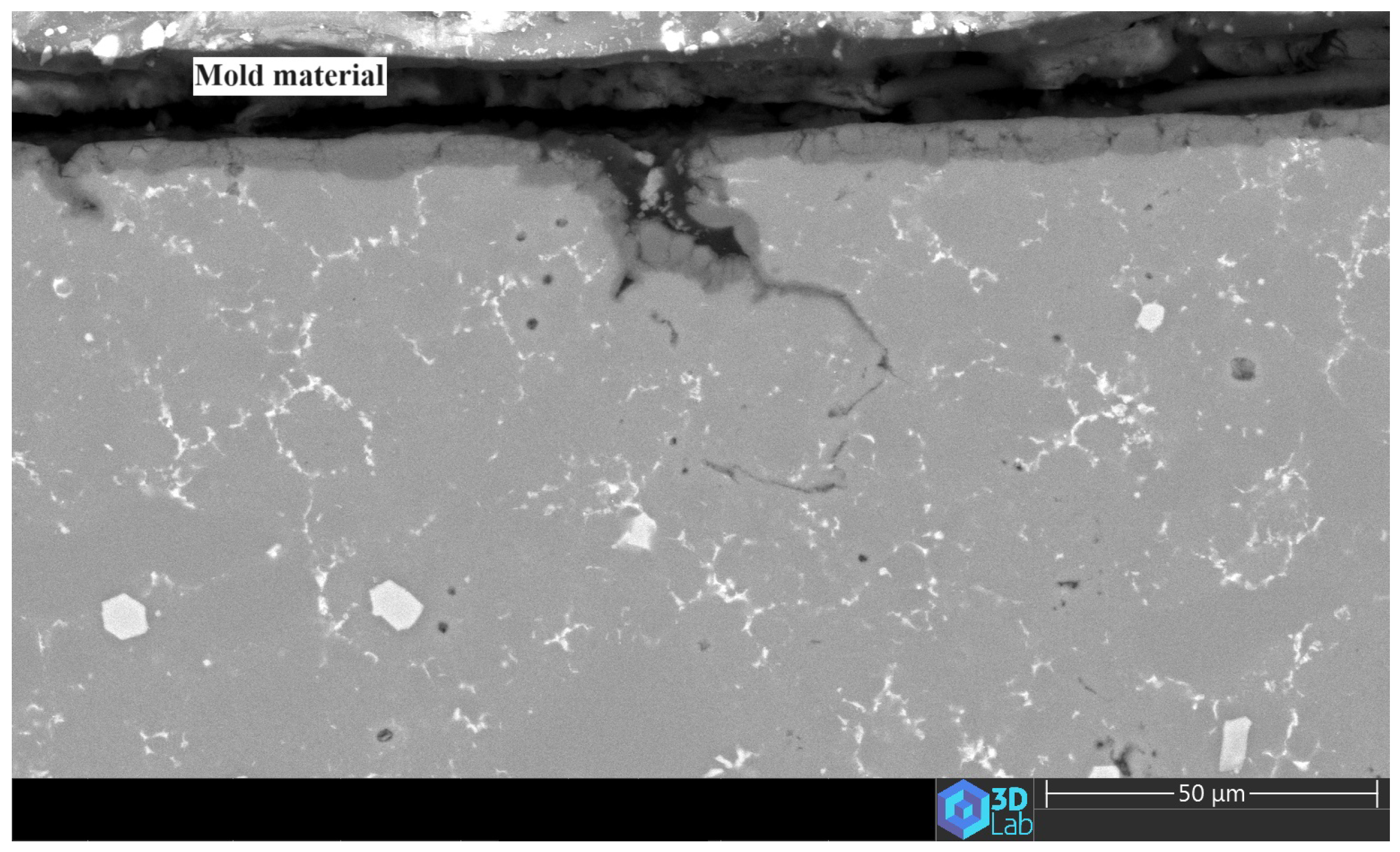
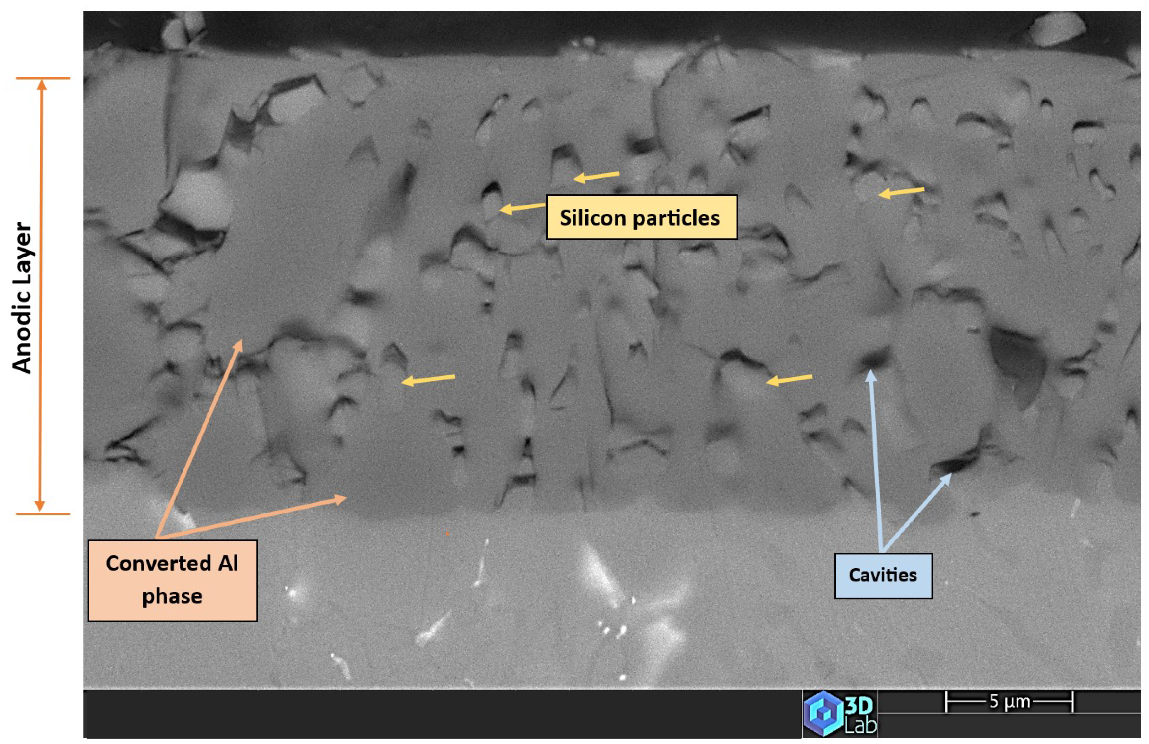
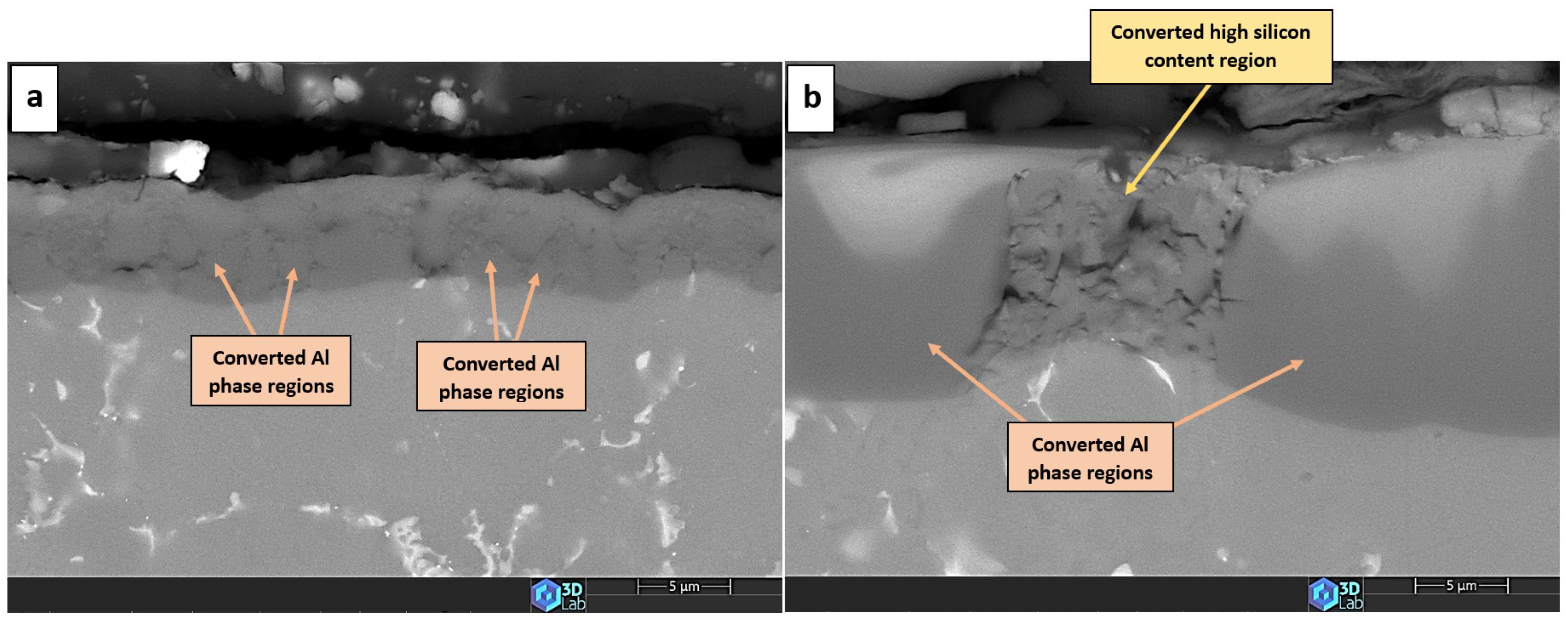
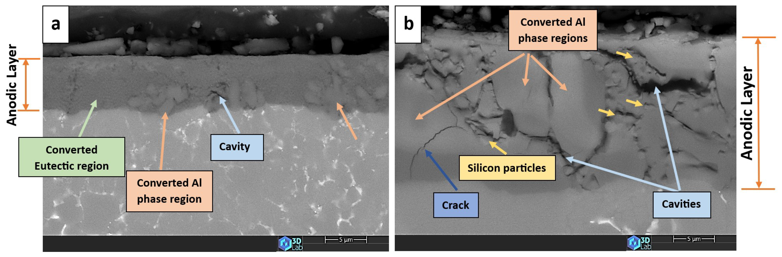
3.4. The Anodic Layer Structures

The anodization process of cast aluminium alloys leads to the formation of oxidized surfaces characterized by lower quality, primarily due to elevated levels of silicon (Si) and other elements like iron (Fe) and copper (Cu) [31]. The presence of surface defects; intermetallic, eutectic segregation; and surface liquid segregation (SLS), which are typical in die castings, induces alterations in the growth, composition, and microstructure of the porous anodic film [16].
Various as-cast substrates can influence the anodization process. Eutectic Si and intermetallic compounds, such as Mg2Si, β -Al5FeSi, α -Al(Fe, Mn, Cr)Si, and Al2Cu phases, prove detrimental to the anodization process [14,16,32,33]. These secondary phases cause localized changes in the composition and morphology of the interface between the bulk material and the oxide, influencing the thickness of the oxide layer [30]. Moreover, certain phases may reduce the hardness and thickness of the anodic film while increasing its porosity [14,32].
The region of the surface affected by Si segregation typically has a thickness of up to approximately 1 mm and exhibits a higher concentration of Al-Si eutectic compared to the center of the casting. Additionally, die castings, though generally near-net shape components, often undergo surface mechanical finishing such as grinding, vibratory treatment, or blasting. Surface machining serves to eliminate surface segregation and many intermetallic particles formed in close proximity to the casting surface [21].
It is evident that the surface defects and heterogeneities mentioned previously are primarily present in areas where the casting surface has not undergone mechanical machining. Depending on the power mode being utilized, the removal of different materials from the surface modifies the structural characteristics and causes a shift in the thickness of the anodic layer. During the anodization process of Al-Si alloy, the presence of eutectic silicon (Si) particles can trigger the development of various defects within the anodic layer. These include the following:
  • Formation of oxygen gas-filled voids: When the oxide front interacts with the silicon phase, it leads to the generation of both SiO2 and gaseous oxygen due to the semiconductor properties of the Si–O bond. Consequently, oxygen gas-filled voids emerge in the aluminium substrate in proximity to the Si particles [31,34].
  • Creation of unanodized zones: Unanodized zones form when the oxide front fails to entirely encircle the Si phase, possibly due to its shape or reduced spacing between particles. Consequently, the eutectic silicon phase acts as a barrier shielding the adjacent Al matrix, preventing it from being reached by the oxide front and thus remaining unanodized. The residual metallic Al phase is predominantly detected beneath or amid coarse and interconnected Si eutectic particles [31].
  • Influence on film cracking and intrinsic stress: Silicon particles can hinder the volumetric expansion of the oxidizing matrix, leading to localized intrinsic stress and the formation of cracks within the film [31,35].
In the case of SSV mode using 35 V, the as-cast surface, owing to its finer structure, reveals smaller converted aluminium regions, whereas the removal of 0.5 mm of material exposes larger converted Al phase regions accompanied by cavity formation, as shown in Figure 9. These cavities, linked to the presence of eutectic silicon particles, manifest as larger in Figure 9b compared to Figure 9a because they relate to the eutectic silicon particles, which are much finer in the as-cast surface. Concurrently, cracks emerge in the converted Al phase.
Similar structural patterns emerge after removing 1 mm of material before anodizing, as seen in Figure 10. The anodic layer’s structure reflects the original material’s configuration, showcasing uniformly converted Al phases and cavities attributed to silicon particles. This consistent behavior persists even at an SSV of 20V, as depicted in Figure 11; a clear structural contrast is evident between the silicon-containing converted region and the converted aluminium phase, where the oxide front advances toward the bulk alloy with more depth compared to the region containing higher silicon eutectic particles.
The structure of anodized samples in SSC mode exhibits the same characteristics. The anodic layer structure resulting from the as-cast surface and after removing 0.5 mm and 1 mm of material, respectively, is shown in Figure 12. Along with homogeneous sections—the converted aluminium—the structure also has inhomogeneous regions and black regions with varying lengths and widths.

4. Conclusions

In this study of die-cast AlSi12Cu1(Fe) alloy, the anodic layer thickness increased following material removal by grinding before the anodizing process. The amount of material removed, up to one millimeter, is directly correlated with the anodic layer thickness increase. The thickness of the anodic layer produced following the grinding of surfaces was notably higher when anodized under SSV at 35 V than that anodized under SSV at 20 V, showing an increase in the range of 2 to 2.5 times more than the thickness of the anodic layer obtained under SSV at 20 V. Furthermore, the anodizing under steady-state current mode (1.6 A·dm−2) resulted in a thicker anodic layer than the anodic layer thickness obtained under steady-state voltage mode (35 V, 1.6 A·dm−2 max) in all initial surface states (as-cast, ground). These findings were substantiated by recording the total apparent charge in both scenarios, showcasing a direct proportionality between the anodic layer thickness and the total apparent charge.
Furthermore, the alterations observed in the anodic layer thickness after surface grinding can be attributed to shifts in the alloy composition. The skin layer exhibits a finer structure, and as the oxide layer progresses deeper into the alloy, notable alterations occur in both the composition and the reactive phase. Grinding the skin layer and accessing areas characterized by a slower solidification rate leads to the presence of a large, homogeneous Al phase. This Al phase, in turn, supports an increased rate of oxide growth. Surface-grinding operations before the anodizing process result in larger cavity sizes. This phenomenon is directly linked to variations in the microstructure composition and the size of the forming phases.

Author Contributions

Conceptualization, T.I.T. and E.R.; methodology, E.R.; software, D.K.-H.; validation, T.I.T., D.K.-H. and E.R.; formal analysis, T.I.T.; investigation, E.R. and D.K.-H.; resources, T.I.T. and D.K.-H.; data curation, D.K.-H. and E.R.; writing—original draft preparation, E.R.; writing—review and editing, T.I.T.; visualization, E.R.; supervision, T.I.T.; project administration, T.I.T.; funding acquisition, T.I.T. and D.K.-H. All authors have read and agreed to the published version of the manuscript.

Funding

This research received no external funding.

Data Availability Statement

Data are contained within the article.

Acknowledgments

The authors would like to acknowledge the support provided by the 3D Laboratory of the University of Miskolc and colleagues Anikó Márkusné and Zoltán Kéri.

Conflicts of Interest

The authors declare that they have no known competing financial interests or personal relationships that could have appeared to influence the work reported in this paper.

References

  1. Casting Source Magazine. Available online: https://www.castingsource.com/articles/2015/11/01/improving-surface-finishing-die-castings (accessed on 1 February 2024).
  2. Runge, J.M. The Metallurgy of Anodizing Aluminum; Springer International Publishing: Chicago, IL, USA, 2018; pp. 344–361. [Google Scholar]
  3. Török, T.I. Anodizing surface treatments of aluminium alloys-Challenges and solutions. BKL Bányászati Kohászati Lapok 2023, 156, 46–50. [Google Scholar]
  4. Chen, J.; Wen, F.; Liu, C.; Li, W.; Zhou, Q.; Zhu, W.; Zhang, Y.; Guan, R. The microstructure and property of Al-Si alloy improved by the Sc-microalloying and Y2O3 nano-particles. Sci. Technol. Adv. Mater. 2021, 22, 205–217. [Google Scholar]
  5. Huang, J.M.; Zhao, H.D.; Chen, Z.M. Microstructure and properties of A356 alloy wheels fabricated by low-pressure die casting with local squeeze. J. Mater. Eng. Perform. 2019, 28, 2137–2146. [Google Scholar]
  6. Martin, J.H.; Yahata, B.D.; Hundley, J.M.; Mayer, J.A.; Schaedler, T.A.; Pollock, T.M. 3D printing of high-strength aluminium alloys. Nature 2017, 549, 365–369. [Google Scholar] [CrossRef]
  7. Cabrini, M.; Lorenzi, S.; Pastore, T.; Testa, C.; Manfredi, D.; Lorusso, M.; Calignano, F.; Pavese, M.; Andreatta, F. Corrosion behavior of AlSi10Mg alloy produced by laser powder bed fusion under chloride exposure. Corros. Sci. 2019, 152, 101–108. [Google Scholar] [CrossRef]
  8. Rogov, A.B.; Lyu, H.; Matthews, A.; Yerokhin, A. AC plasma electrolytic oxidation of additively manufactured and cast AlSi12 alloys. Surf. Coat. Technol. 2020, 399, 126116. [Google Scholar] [CrossRef]
  9. Pezzato, L.; Dabalà, M.; Gross, S.; Brunelli, K. Effect of microstructure and porosity of AlSi10Mg alloy produced by selective laser melting on the corrosion properties of plasma electrolytic oxidation coatings. Surf. Coat. Technol. 2020, 404, 126477. [Google Scholar]
  10. Zhu, B.; Zanella, C. Hardness and corrosion behaviour of anodised Al-Si produced by rheocasting. Mater. Des. 2019, 173, 107764. [Google Scholar] [CrossRef]
  11. Lien, H.H.; Mazumder, J.; Wang, J.; Misra, A. Microstructure evolution and high density of nanotwinned ultrafine Si in hypereutectic Al-Si alloy by laser surface remelting. Mater. Charact. 2020, 161, 110147. [Google Scholar] [CrossRef]
  12. Mora-Sanchez, H.; Del Olmo, R.; Rams, J.; Torres, B.; Mohedano, M.; Matykina, E.; Arrabal, R. Hard anodizing and plasma electrolytic oxidation of an additively manufactured Al-Si alloy. Surf. Coat. Technol. 2021, 420, 127339. [Google Scholar] [CrossRef]
  13. Wang, P.; Ma, Q.; Yuwen, Q.; Li, J. The differences in the formation mechanism of PEO and CPED composited ceramic coatings on Al-12Si alloy. J. Alloys Compd. 2019, 788, 61–66. [Google Scholar] [CrossRef]
  14. Konieczny, J.; Dobrzański, L.A.; Labisz, K.; Duszczyk, J. The influence of cast method and anodizing parameters on structure and layer thickness of aluminium alloys. J. Mater. Process. Technol. 2004, 157, 718–723. [Google Scholar] [CrossRef]
  15. Bouchama, L.; Azzouz, N.; Boukmouche, N.; Chopart, J.P.; Daltin, A.L.; Bouznit, Y. Enhancing aluminium corrosion resistance by two-step anodizing process. Surf. Coat. Technol. 2013, 235, 676–684. [Google Scholar] [CrossRef]
  16. Tsangaraki-Kaplanoglou, I.; Theohari, S.; Dimogerontakis, T.; Wang, Y.M.; Kuo, H.H.H.; Kia, S. Effect of alloy types on the anodizing process of aluminium. Surf. Coat. Technol. 2006, 200, 2634–2641. [Google Scholar] [CrossRef]
  17. Caliari, D.; Timelli, G.; Zabala, B.; Igartua, A. Microstructural and tribological investigations of diecast and hard anodized AlSiCu alloys. Surf. Coat. Technol. 2018, 352, 462–473. [Google Scholar] [CrossRef]
  18. Shang, Y.; Wang, L.; Liu, Z.; Niu, D.; Wang, Y.; Liu, C. The Effects of Different Sealing Techniques for Anodic Film of Al-12.7 Si 0.7 Mg Alloys. Int. J. Electrochem. Sci. 2016, 11, 5234–5344. [Google Scholar]
  19. Arrabal, R.; Mingo, B.; Pardo, A.; Mohedano, M.; Matykina, E.; Rodríguez, I. Pitting corrosion of rheocast A356 aluminium alloy in 3.5 wt.% NaCl solution. Corros. Sci. 2013, 73, 342–355. [Google Scholar]
  20. Mingo, B.; Arrabal, R.; Pardo, A.; Matykina, E.; Skeldon, P. 3D study of intermetallics and their effect on the corrosion morphology of rheocast aluminium alloy. Mater. Charact. 2016, 112, 122–128. [Google Scholar] [CrossRef]
  21. Caliari, D.; Timelli, G.; Salata, T.; Cavagnini, G.; Maestri, S. Surface defects of anodized HPDC Al alloy components. Metall. Ital. 2016, 108, 69–72. [Google Scholar]
  22. Fratila-Apachitei, L.E.; Duszczyk, J.; Katgerman, L. Vickers microhardness of AlSi (Cu) anodic oxide layers formed in H2SO4 at low temperature. Surf. Coat. Technol. 2003, 165, 309–315. [Google Scholar] [CrossRef]
  23. Grosselle, F.; Timelli, G.; Bonollo, F.; Molina, R. Correlation between microstructure and mechanical properties of Al-Si diecast engine blocks. Metall. Sci. Technol. 2009, 27, 5–6. [Google Scholar]
  24. Zhu, B.W.; Seifeddine, S.; Jarfors, A.E.; Leisner, P.; Zanella, C. A study of anodising behaviour of Al-Si components produced by rheocasting. Solid State Phenom. 2019, 285, 39–44. [Google Scholar] [CrossRef]
  25. Zhang, F.; Örnek, C.; Nilsson, J.O.; Pan, J. Anodisation of aluminium alloy AA7075–Influence of intermetallic particles on anodic oxide growth. Corros. Sci. 2020, 164, 108319. [Google Scholar] [CrossRef]
  26. Scampone, G.; Timelli, G. Anodizing Al–Si foundry alloys: A critical review. Adv. Eng. Mater. 2022, 24, 2101480. [Google Scholar] [CrossRef]
  27. Dong, H. Surface Engineering of Light Alloys: Aluminium. Magnesium and Titanium Alloys; Woodhead Publishing: New York, NY, USA, 2010; pp. 84–86. [Google Scholar]
  28. Labisz, K.; Dobrzański, L.A.; Konieczny, J. Anodization of cast aluminium alloys produced by different casting methods. Arch. Foundry Eng. 2008, 8, 45–50. [Google Scholar]
  29. Riddar, F.; Hogmark, S.; Rudolphi, Å.K. Comparison of anodised aluminium surfaces from four fabrication methods. J. Mater. Process. Technol. 2012, 212, 2272–2281. [Google Scholar] [CrossRef]
  30. Abrahami, S.T. Cr (VI)-Free Pre-Treatments for Adhesive Bonding of Aerospace Aluminium Alloys. Ph.D. Thesis, Delft University of Technology, Delft, The Netherlands, 2016. [Google Scholar]
  31. Zhu, B.; Seifeddine, S.; Persson, P.O.; Jarfors, A.E.; Leisner, P.; Zanella, C. A study of formation and growth of the anodised surface layer on cast Al-Si alloys based on different analytical techniques. Mater. Des. 2016, 101, 254–262. [Google Scholar] [CrossRef]
  32. Shin, J.S.; Kim, B.H.; Lee, S.M. Effects of physical melt treatments on microstructural evolution and anodizing characteristics of Al-Si casting alloys. Mater. Sci. Forum 2011, 695, 243–246. [Google Scholar] [CrossRef]
  33. Chauke, L.; Möller, H.; Govender, G. Anodizing of aluminium alloy plates from different series produced by rheo-high pressure die casting. Solid State Phenom. 2015, 217, 247–252. [Google Scholar]
  34. Fratila-Apachitei, L.E.; Tichelaar, F.D.; Thompson, G.E.; Terryn, H.; Skeldon, P.; Duszczyk, J.; Katgerman, L. A transmission electron microscopy study of hard anodic oxide layers on AlSi (Cu) alloys. Electrochim. Acta 2004, 49, 3169–3177. [Google Scholar] [CrossRef]
  35. Fratila-Apachitei, L.E.; Duszczyk, J.; Katgerman, L. Voltage transients and morphology of AlSi (Cu) anodic oxide layers formed in H2SO4 at low temperature. Surf. Coat. Technol. 2022, 157, 80–94. [Google Scholar]
Figure 1. Voltage–current density profile of a die-cast samples (as-cast) as a function of anodization time at steady-state voltage of (a) 35 V and (b) 20 V, respectively.
Crystals 14 00352 g001
Figure 2. Voltage–current density profile of a die-cast sample (as-cast) as a function of anodization time at a steady-state current of 1.6 A·dm−2.
Crystals 14 00352 g002
Figure 3. SEM micrographs of the cross section depicting some defects at the surface region and the heterogeneous microstructure.
Crystals 14 00352 g003
Figure 4. Variation in oxide layer thickness in the different experimental configurations.
Crystals 14 00352 g004
Figure 5. SEM-EDS map micrographs of the cross section of the as-cast anodized sample under SSV mode using 20 V; the anodic layer thickness is 3 µm.
Crystals 14 00352 g005
Figure 6. EDS for sample VM12: (a) EDS map micrographs of the cross section; (b) silicon distribution; (c) aluminium distribution; (d) oxygen distribution; (e) sulfur distribution; (f) carbon distribution; (g) iron distribution; (h) copper distribution.
Crystals 14 00352 g006aCrystals 14 00352 g006b
Figure 7. Element profile plot of the alloying elements for sample VM22.
Crystals 14 00352 g007aCrystals 14 00352 g007b
Figure 8. Element profile plot of the alloying elements for sample CM2.
Crystals 14 00352 g008
Figure 9. The anodized layer structure obtained under a steady-state voltage of 35 V. (a) The as-die-cast surface, sample VC1. (b) The ground surface, removing 0.5 mm of material, sample VM12.
Crystals 14 00352 g009
Figure 10. The anodized layer structure obtained under a steady-state voltage of 35 V after removing 1 mm of material, sample VM13.
Crystals 14 00352 g010
Figure 11. The anodized layer structure obtained under a steady-state voltage of 20 V. (a) The as-die-cast surface, sample VC2. (b) The ground surface, removing 1 mm of material, sample VM23.
Crystals 14 00352 g011
Figure 12. The anodized layer structure obtained under a steady-state current of 1.6A·dm−2 for (a) the as-cast surface, sample CC1; (b) the ground surface, removing 0.5 mm of material, sample CM2; (c) the ground surface, removing 1mm of material, sample CM3.
Crystals 14 00352 g012
Table 1. Description of the anodizing process parameters for tested samples.
SampleSurface ConditionAnodizing StateAnodizing Duration (min)Theoretical Current Density(max) (A·dm−2)Apparent Charge (A·s)
VC1As-CastSSV (35 V)601.648
VM11ground (−0.1 mm)SSV (35 V)602.356
VM12ground (−0.5 mm)SSV (35 V)602.458
VM13ground (−1 mm)SSV (35 V)602.874
VC2As-CastSSV (20 V)600.728
VM21ground (−0.1 mm)SSV (20 V)600.732
VM22ground (−0.5 mm)SSV (20 V)600.732
VM23ground (−1 mm)SSV (20 V)600.937
CC1As-CastSSC601.690
CM1ground (−0.1 mm)SSC601.690
CM2ground (−0.5 mm)SSC601.690
CM3ground (−1 mm)SSC601.690
Disclaimer/Publisher’s Note: The statements, opinions and data contained in all publications are solely those of the individual author(s) and contributor(s) and not of MDPI and/or the editor(s). MDPI and/or the editor(s) disclaim responsibility for any injury to people or property resulting from any ideas, methods, instructions or products referred to in the content.

