Article

Manufacturing of TiO2, Al2O3 and Y2O3 Ceramic Nanotubes for Application as Electrodes for Printable Electrochemical Sensors

by
Alexandru Florentin Trandabat
,
Romeo Cristian Ciobanu
*,
Oliver Daniel Schreiner
,
Mihaela Aradoaei
and
Sebastian Teodor Aradoaei
Department of Electrical Measurements and Materials, Gheorghe Asachi Technical University, 700050 Iasi, Romania
*
Author to whom correspondence should be addressed.
Crystals 2024, 14(5), 454; https://doi.org/10.3390/cryst14050454
Submission received: 23 April 2024 / Revised: 9 May 2024 / Accepted: 10 May 2024 / Published: 11 May 2024
(This article belongs to the Special Issue Metal Oxide Thin Films, Nanomaterials and Nanostructures)

Abstract

:
This paper describes the process to obtain ceramic nanotubes from titanium dioxide, alumina and yttrium oxide by a feasible, replicable and reliable technology, including three stages, starting from an electrospinning process of poly(methyl methacrylate) solutions. A minimum diameter of 0.3 μm was considered optimal for PMMA nanofibers in order to maintain the structural stability of covered fibers, which, after ceramic film deposition, leads to a fiber diameter of 0.5–0.6 μm. After a chemical and physical analysis of the stages of obtaining ceramic nanotubes, in all cases, uniform deposition of a ceramic film on PMMA fibers and, finally, a uniform structure of ceramic nanotubes were noted. The technological purpose was to use such nanotubes as ingredients in screen-printing inks for electrochemical sensors, because no study directly targeted the subject of ceramic nanotube applications for printed electronics to date. The printing technology was analyzed in terms of the ink deposition process, printed electrode roughness vs. type of ceramic nanotubes, derived inks, thermal curing of the electrodes and the conductivity of electrodes on different support (rigid and flexible) at different curing temperatures. The experimental inks containing ceramic nanotubes can be considered feasible for printed electronics, because they offer fast curing at low temperatures, reasonable conductivity vs. electrode length, good printability on both ceramic or plastic (flexible) supports and good adhesion to surface after curing.

1. Introduction

Metal oxides exhibit several key advantages for multiple applications, such as sensors, solar cells, cathode material for batteries, and photocatalysis, which has encouraged researchers’ efforts to improve their technology and architecture. But the considerable difficulties encountered in obtaining ceramic thin films, respectively ceramic nanotubes, prevented their large-scale manufacture.
Although there are some studies on ceramic nanotubes technology from the last 15 years, e.g., [1,2,3,4,5,6,7,8,9,10,11], no study directly targeted the subject of ceramic nanotube composites. Some papers addressed, e.g., carbon–ceramic nanotube composites and ceramic nanoparticles associated with carbon nanotubes, as in [12,13,14,15,16,17,18,19]. On the other hand, no study directly targeted the subject of ceramic nanotube applications for printed electronics, e.g., printed sensors based on specific inks including ceramic nanotubes, which is the subject of the present paper. Nanotube-based devices change their conductivity due to surface adsorption when exposed to chemical species [20,21]. The same adsorption on the surface may be also present in the case of biomolecules such as amino acids and proteins, which means that the nanotubes are also applicable for the detection of bio-agents [22,23]. The main problem is that most of the authors addressed the surface properties of carbon nanotubes, but none targeted the homologue properties of ceramic nanotubes. The surface architecture of ceramic nanotubes represents a critical element that may impact the future development of sensor applications.
Electrospinning is a high-throughput, cost-effective, and versatile technology used for the manufacturing of nanofiber nets of a large pellet of polymers by applying an electrostatic force [24,25]. Systematic investigations on the effect of electrospinning parameters on fiber diameter and morphology have been reported by several researchers [25,26,27,28]. The major factors controlling the diameter of the fibers are: (1) the concentration of the polymer in the solution, (2) the type of solvent used, (3) the conductivity of the solution, and (4) the solution feed rate. Recently, it has been established that the nature of the collector significantly influences the morphological and physical characteristics of spun fibers [29,30]. The density of fibers per unit area on the collector and the arrangement of the fibers is affected by the degree of charge dissipation upon fiber deposition. The most commonly used target is the conductive metal plate, which results in the collection of randomly oriented fibers in a nonwoven form. Electrospun polymer nanofibers can be further used in the manufacturing process of hollow tubes, in particular ceramic nanotubes. The process implies coating the polymer nanofiber nets with metallic oxides, followed by the removal of the fiber core. Radiofrequency magnetron sputtering is a common deposition technique used to obtain controlled thin films with high technological reproducibility, and can be successfully used for coating polymer nanofiber nets with the metallic oxides [31,32,33,34,35,36]. There are some ceramic nanotubes described in the literature, from simple ceramic nanotubes, such ZnO, CuO, Co3O4, SnO2, MnO2 or TiO2 nanotubes, to more complex ceramic nanotubes, such as Li3V2(PO4)3, Na0.7Fe0.77Mn0.3O2, LiMn2O4, LiCoO2, NiCo2O4 or LiV3O8, based on fabrication processes of large spectrum, e.g., electrodeposition [37,38], hydrothermal [39,40], precipitation [41,42], electrospinning combined with calcination [43,44], and atomic layer deposition [45,46].
In our research titanium, aluminum and yttrium oxides were analyzed in order to obtain uniform ceramic nanotubes by a feasible, replicable and reliable technology, in order to use such nanotubes as ingredients in screen-printing inks dedicated to printed electronics, with further target on innovative nano-sensor development.

2. Technology for Obtaining Ceramic Nanotube Nets

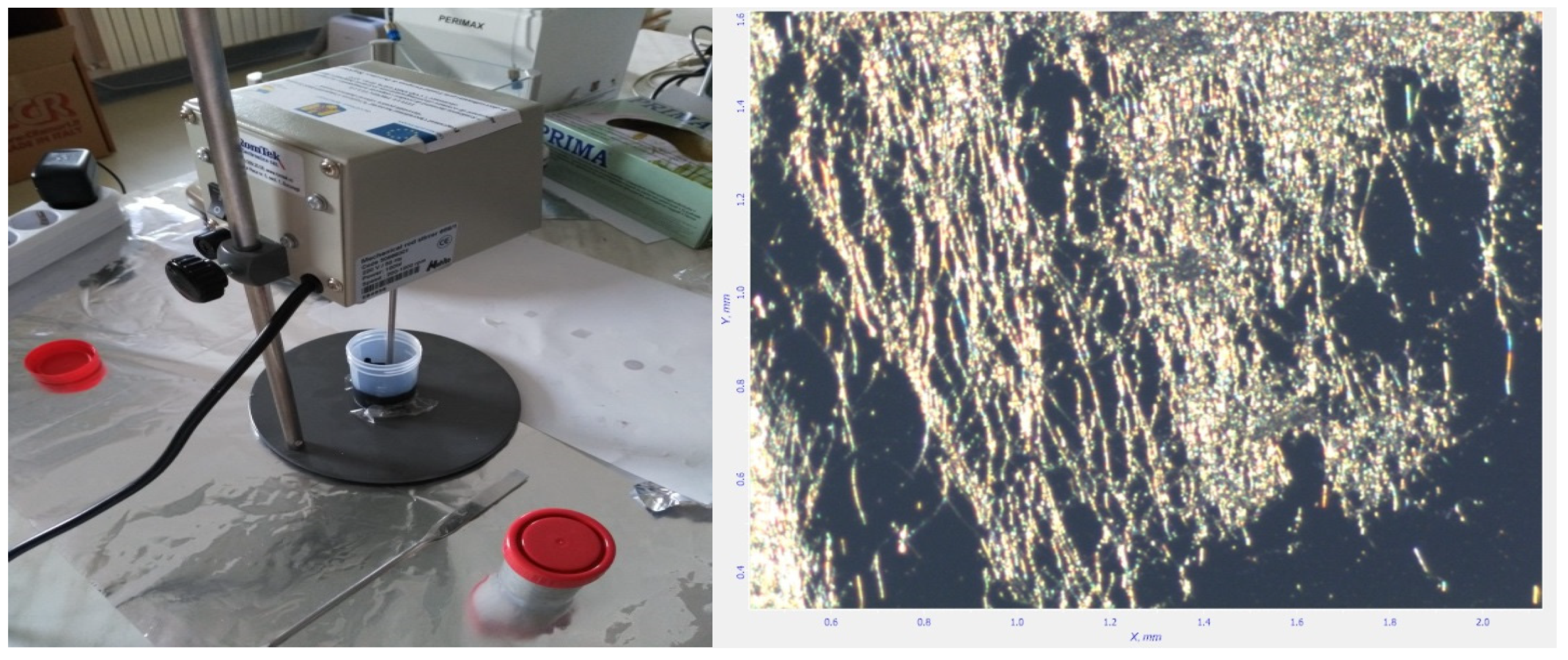
2.1. Technological Equipment

Neu-Pro-BM equipment (TongLiTech, Wuhan, China) was used for the electrospinning process of poly(methyl methacrylate) nanofibers (PMMA nanofibers).
A Tectra Sputter Coater (Tectra GmbH Physikalische Instrumente, Frankfurt, Germany) was the equipment used for radiofrequency (RF) magnetron sputtering.
A Forced convection chamber furnace up to 800 °C (Nabertherm GmbH, Lilienthal, Germany) was used for the PMMA calcination process.
A Keko P200A (Keko Equipment, Žužemberk, Slovenia) screen-printer equipment for printed electronics was used for nanostructured inks testing.

2.2. Materials and Preparation Method

All chemical constituents (ceramic powders and polymers) were procured from Merck (Darmstadt, Germany), and Kurt J. Lesker Company Ltd. (Hastings, UK), and employed without additional refinement. The nanostructured inks were purchased from NovaCentrix, Austin, TX, USA.
The technology of manufacturing TiO2, Al2O3 and Y2O3 ceramic nanotubes was based on three stages, according to the general description in [3,4], and included:
(i)
Preliminary manufacturing of polymer fibers nets of poly(methyl methacrylate) (PMMA), with a molecular weight (Mw) of 300,000, from a solution of 10 wt%, with dimethylformamide (DMF) as solvent.
An experimental plan was conceived, as described in Table 1, with different technological parameters: 5% and 10% concentration of PMMA solution; voltages of 12, 15 and 20 kV were applied; the distance between the needle and the drum was set to 80 and 100 mm; the flow was of 1 mL/h (1 h total time of processing) and the rotation speed of the drum varied between 0 and 5 rpm. The electrospun nanofibers are randomly deposited on a fixed support in the form of a square Cu metal frame (20 × 20 cm2) attached to the collector.
The samples were analyzed under the optical microscope where the dimensions of the microstructure, material defects and cracks were studied.
Figure 1 shows the microscopic image of the nanofibers obtained by using the PMMA solution of 10% and an applied voltage of 12 kV, the distance between the needle and the drum being 100 mm. The average size of the obtained fiber was 0.262 μm.
Figure 2 shows the microscopic image of the nanofibers obtained using the PMMA solution of 10% and an applied voltage of 15 kV, the distance between the needle and the drum being also 100 mm. The size of the fiber obtained was between 0.282 and 0.288 μm.
Figure 3 shows the image obtained under the microscope of the nanofibers obtained by using the PMMA solution of 10% and an applied voltage of 20 kV, the distance between the needle and the drum being also 100 mm. The average size of the obtained fibers was 0.327 μm.
In all, the best results were obtained using a 10% PMMA solution at voltages of 20 kV, with a drum rotation speed of 5 rpm, because the fiber nets were more homogenous as spatial deposition, and also more homogenous as diameter. On the other hand, due to the characteristics of ceramic thin films to be deposited on PMMA nanofibers, a minimum diameter of 0.3 μm was consider optimal for PMMA nanofibers in order to maintain the structural stability of covered fibers from the mechanical point of view.
(ii)
Magnetron deposition of ceramic films
The copper frames housing the PMMA nanofibers nets underwent dual-sided coating with ceramic thin films via RF magnetron sputtering. During the deposition process, ceramic targets with dimensions of 2 inches in diameter and 0.125 inches in thickness was employed. For all involved oxides, the deposition duration for each side was 1 h, and the RF power applied to the magnetron was 200 W. Within the deposition chamber, an argon atmosphere with a purity of 99.99% as working gas, at a pressure of 5.4 × 10⁻³ mbar, was assured.
In Figure 4, the evolution of the dimensions of nanofibers is presented, before and after ceramic film deposition, indicating an increase from approximately 0.327 μm to approximately 0.540 μm.
(iii)
Thermal treatment of nanotubes
Subsequent to this process, the PMMA nanofibers nets, coated on both sides with ceramic films, were transferred onto a Si/SiO2 substrates (cleaned beforehand with acetone and isopropyl alcohol and dry under an argon jet) and subjected to a calcination process conducted at 600 °C for a duration of 12 h in ambient air at atmospheric pressure. Following this procedure, three-dimensional web-like networks of TiO2, Al2O3 and Y2O3 nanotubes were achieved, after the complete combustion of PMMA support.

2.3. Characterization Equipment

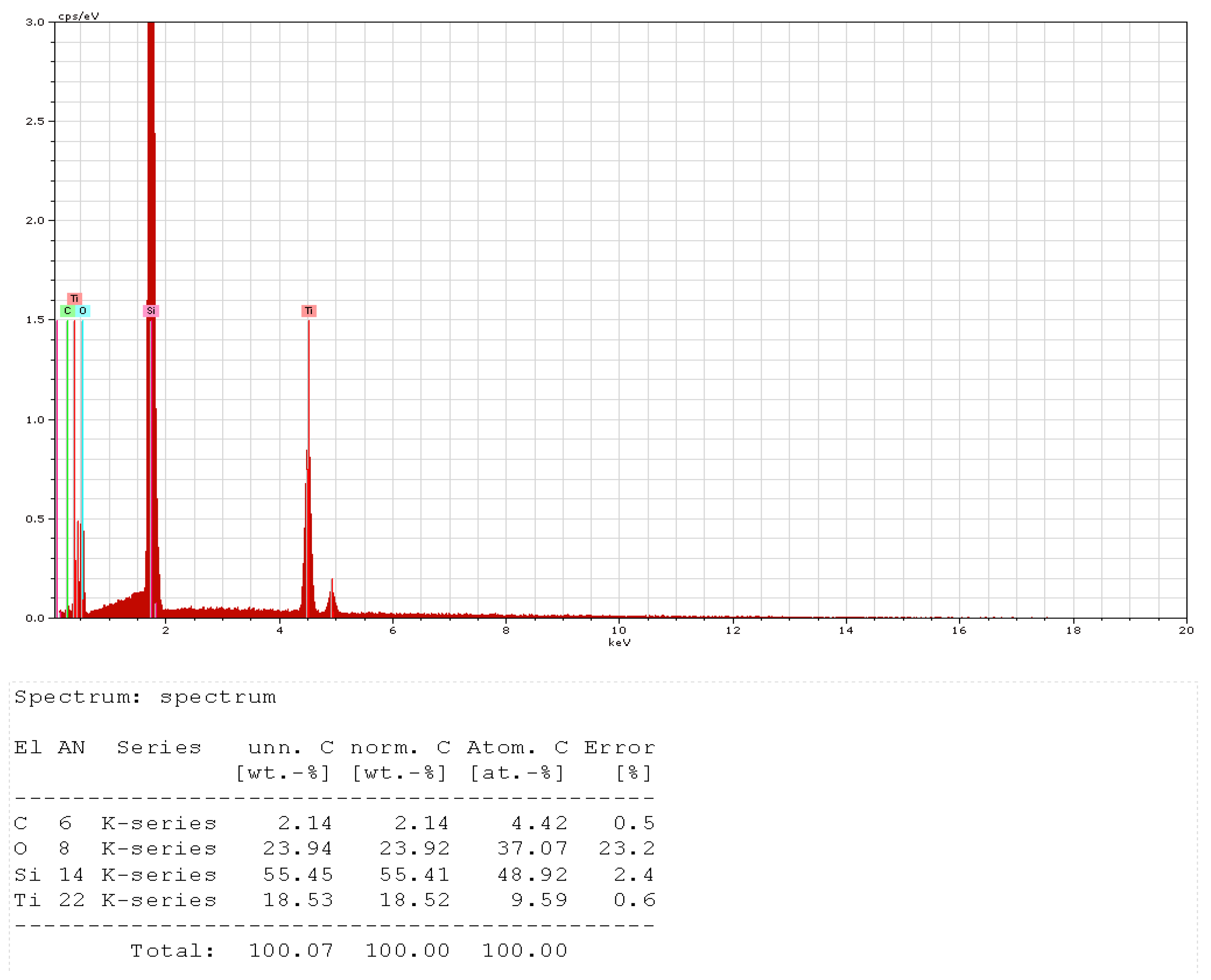
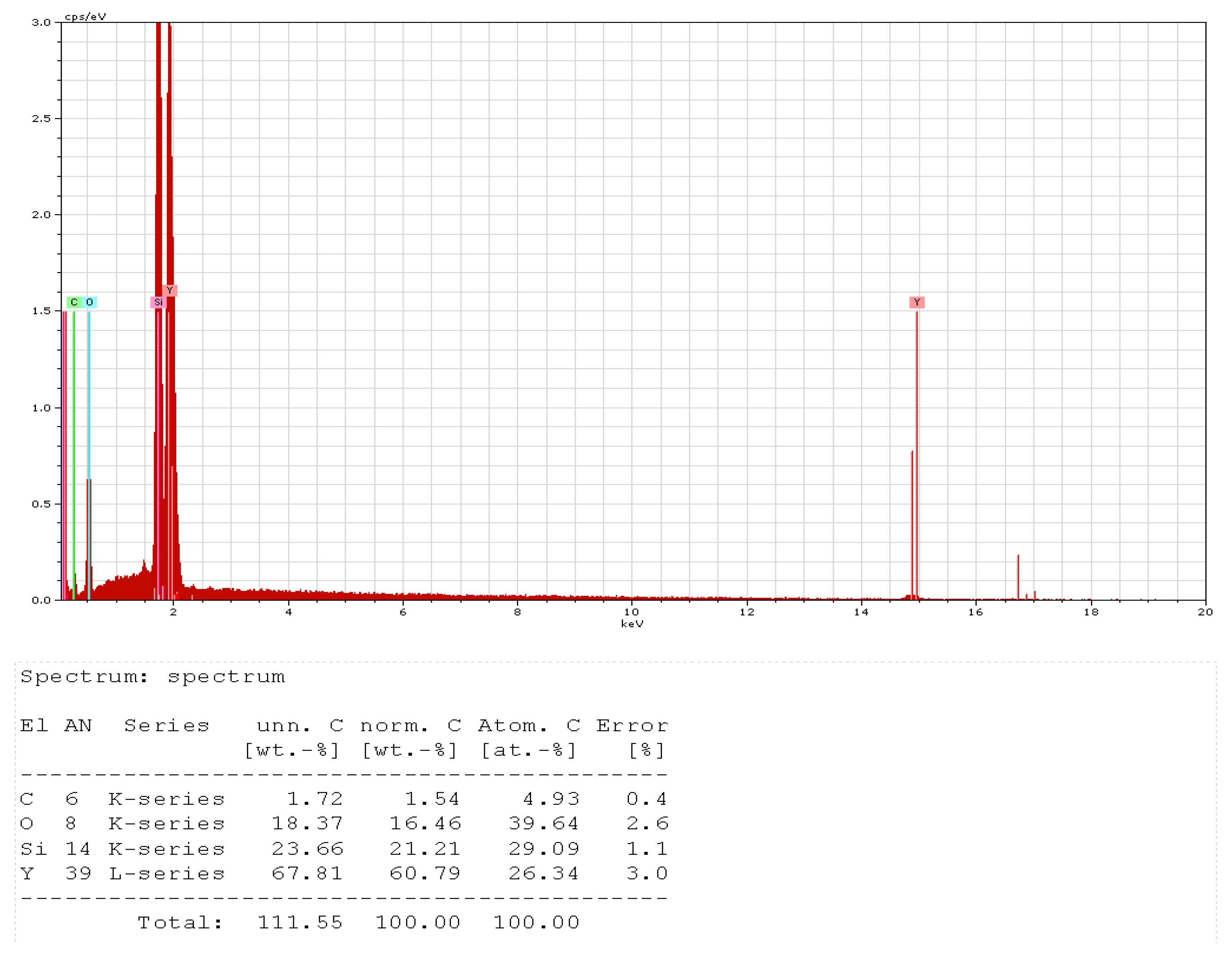
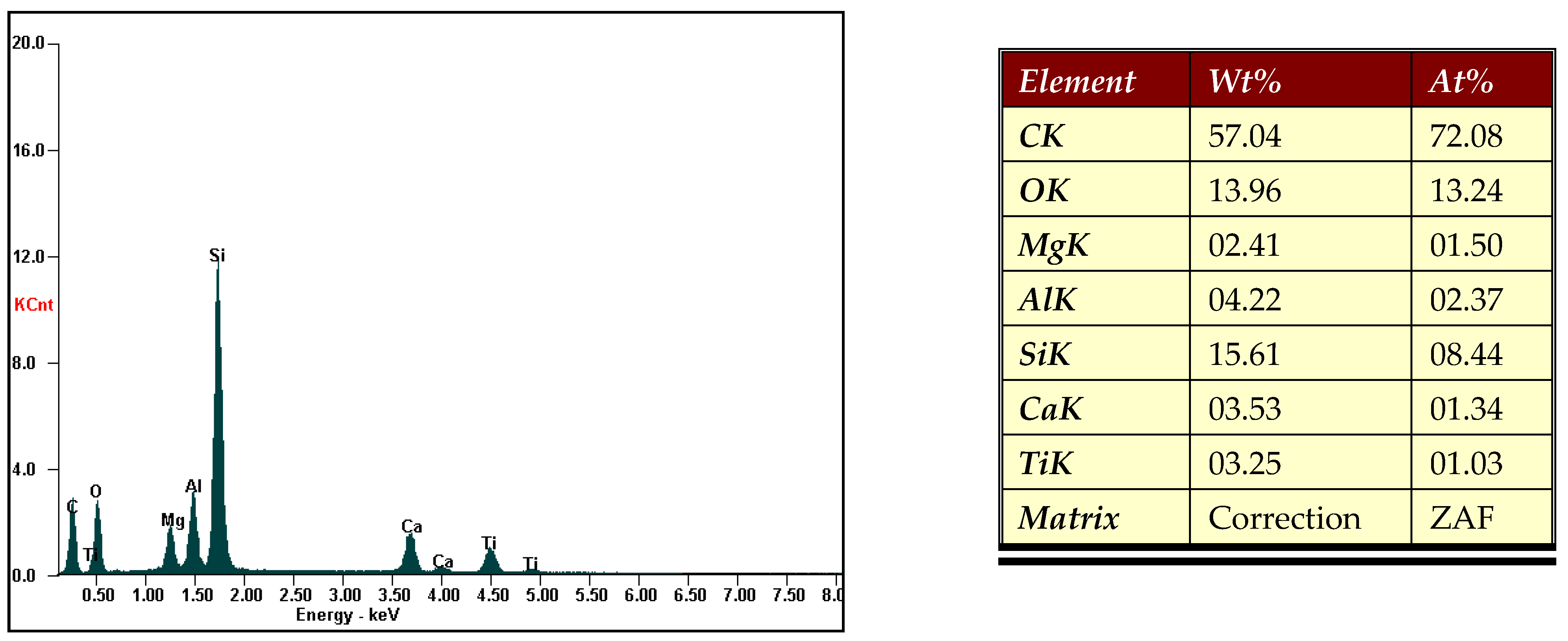
  • Optical scanning microscopy SEM and energy-dispersive X-ray spectroscopy (EDX) were performed with a field emission and focused ion beam scanning electron microscope (SEM) model Tescan Lyra III XMU (Libušina tř. 21 623 00, Brno-Kohoutovice, Czech Republic).
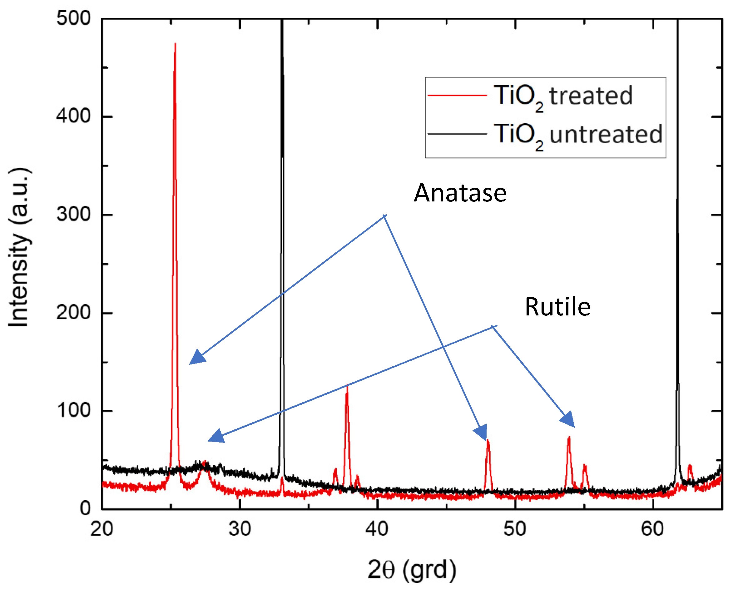
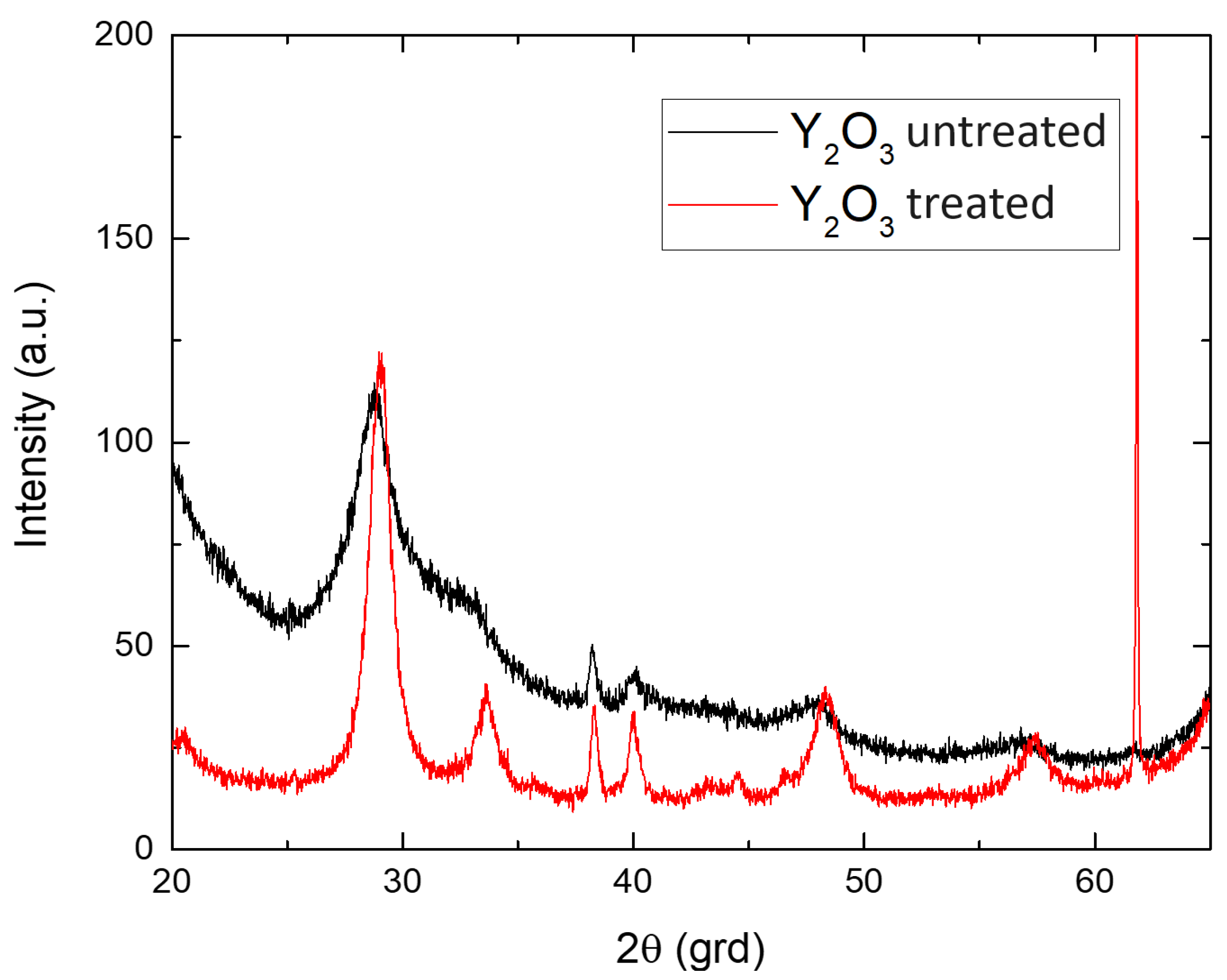
  • Structural characterization was carried out by X-ray diffraction (XRD) using CuKα radiation with Ni filter Bruker AXS D8 Advance (Bruker AXS, Billerica, MA, USA) with CuKα radiation (λ = 0.154 nm). Diffraction patterns were recorded at room temperature in Bragg-Brentano geometry at an angle 2θ from 20° to 65° at a rate of 0.6°/min (2θ)/min.

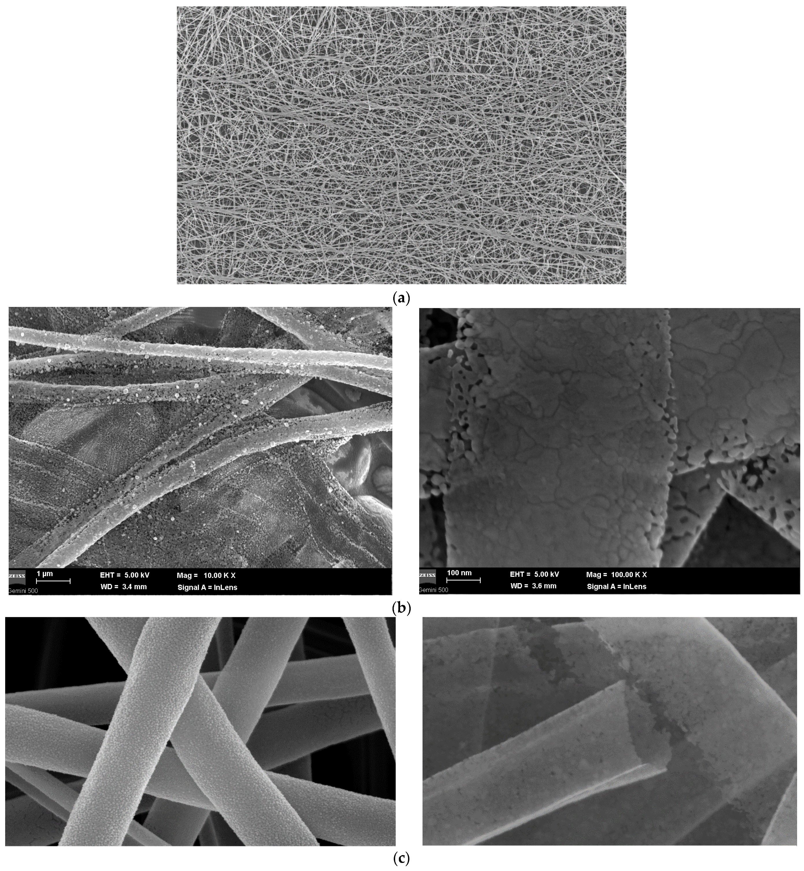
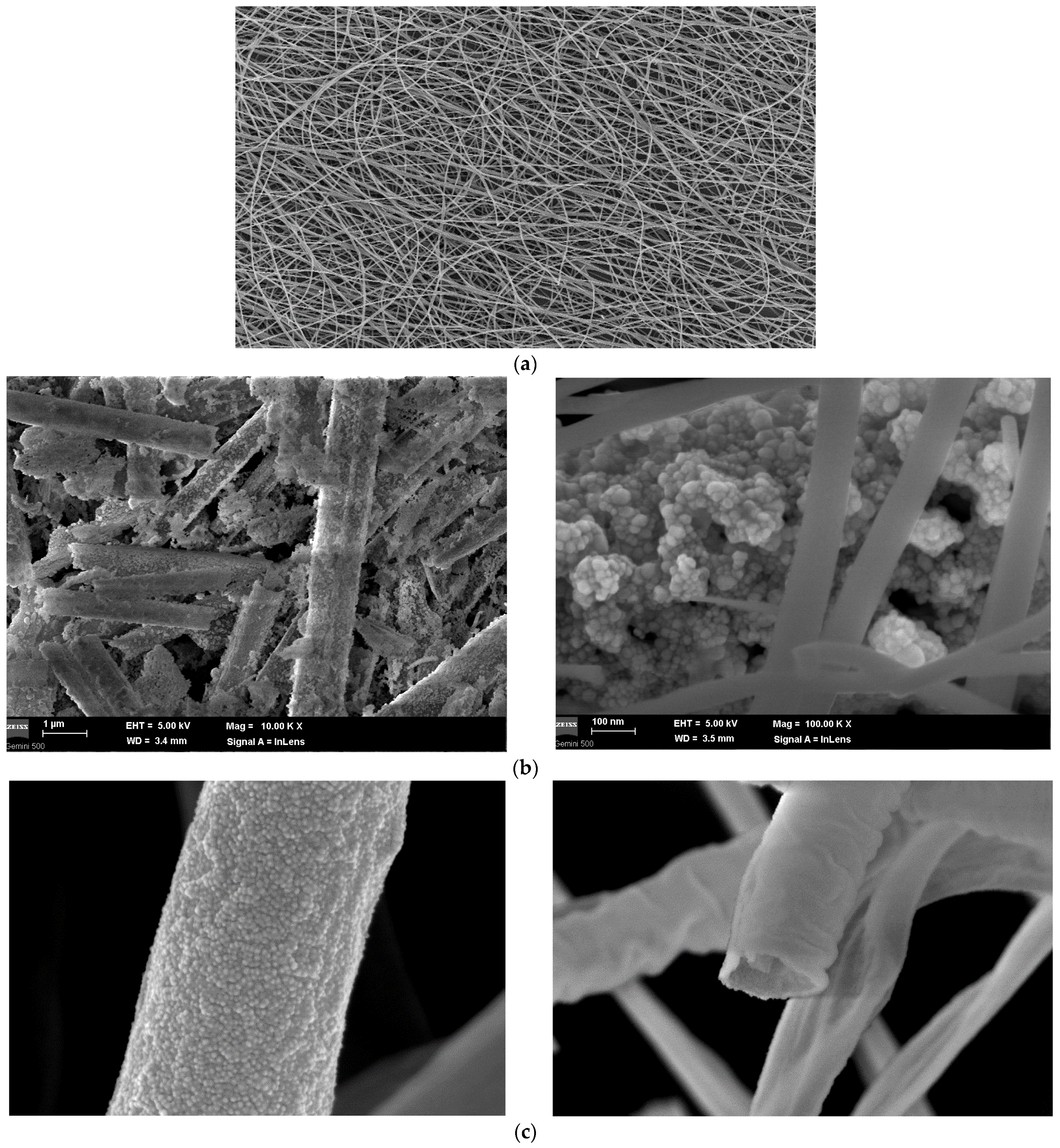
2.4. Results and Discussion
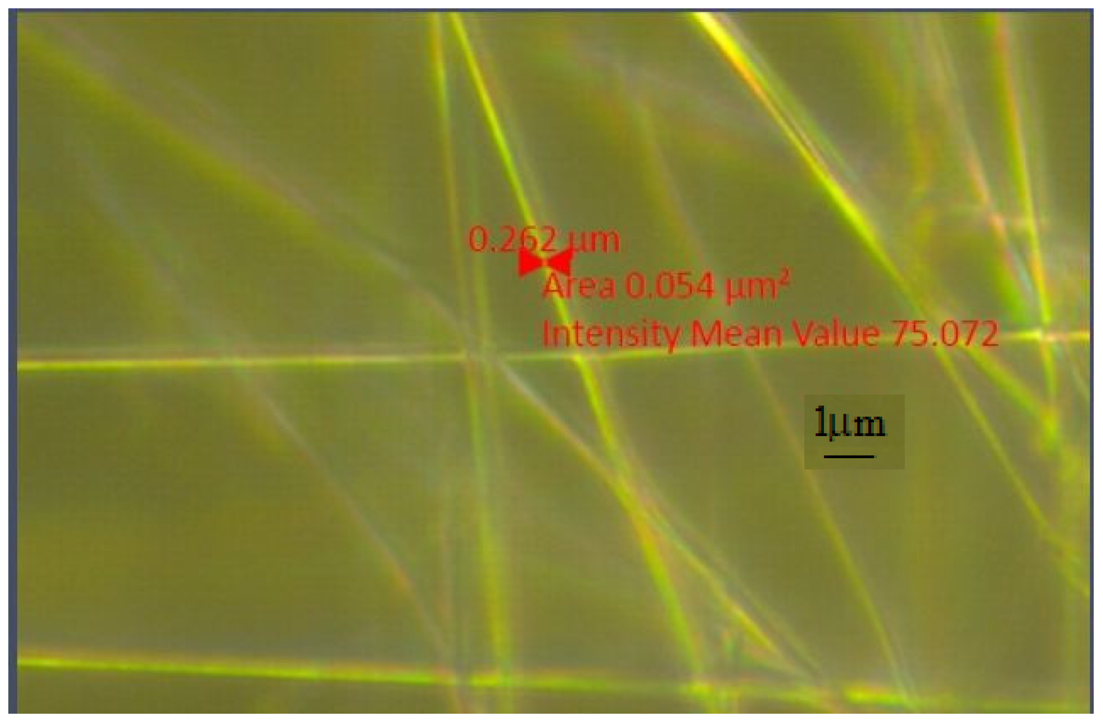
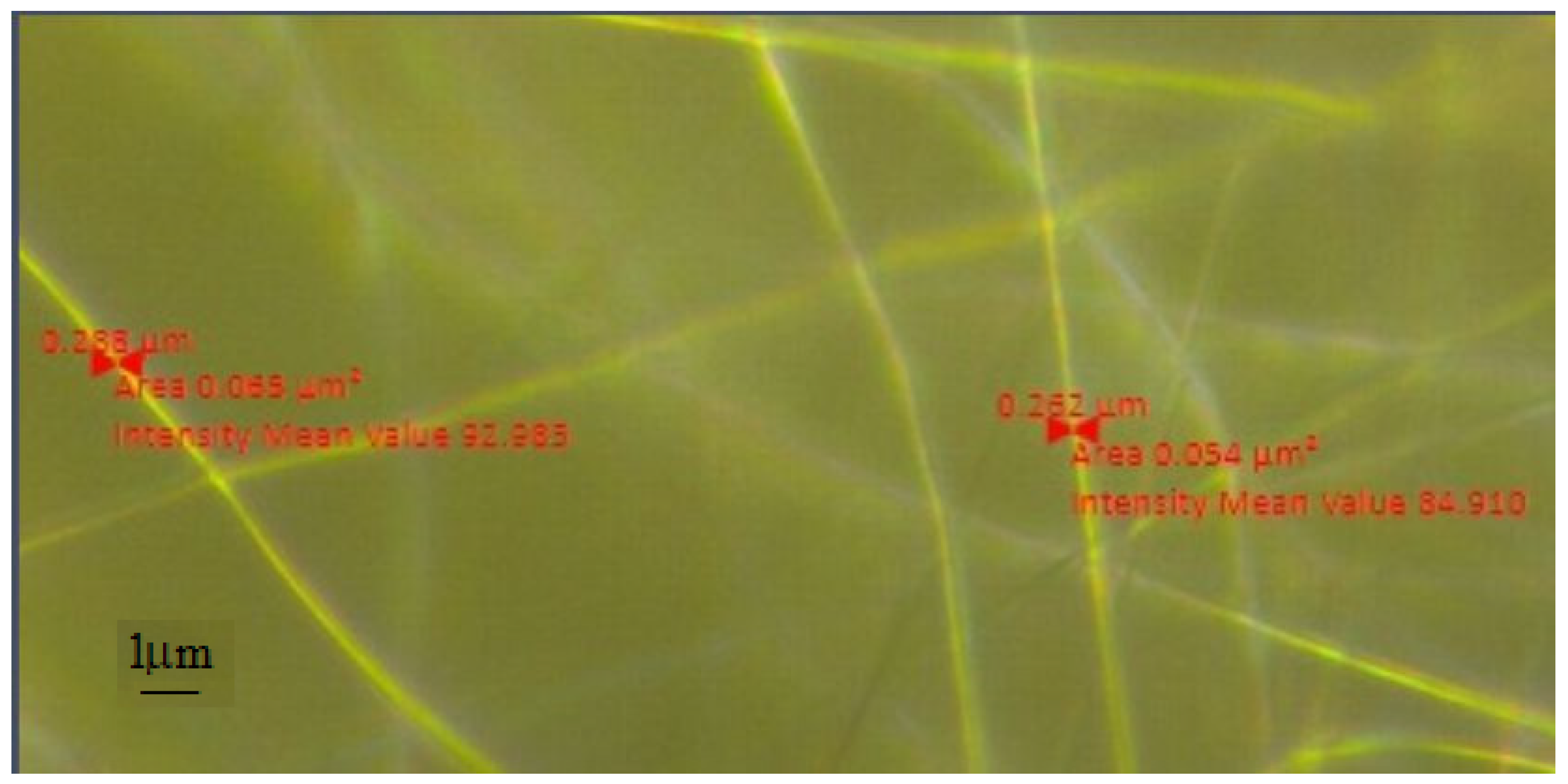
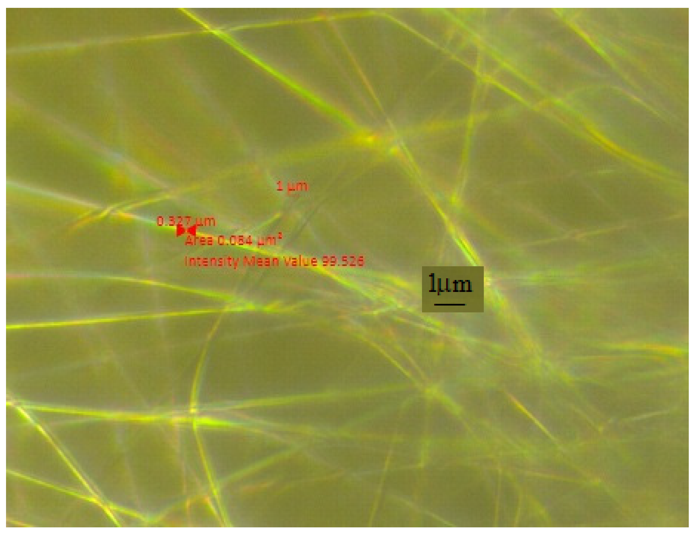
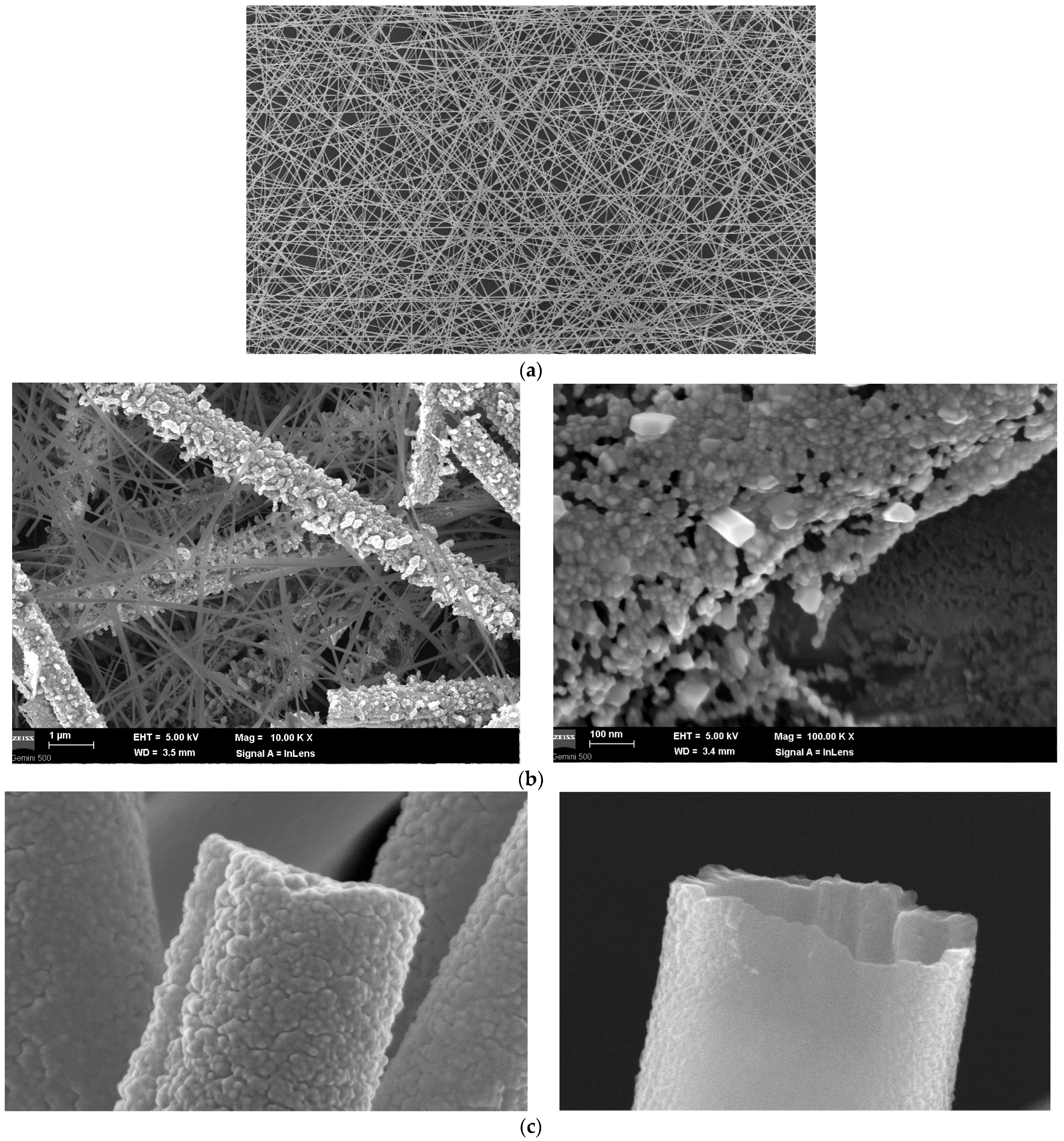
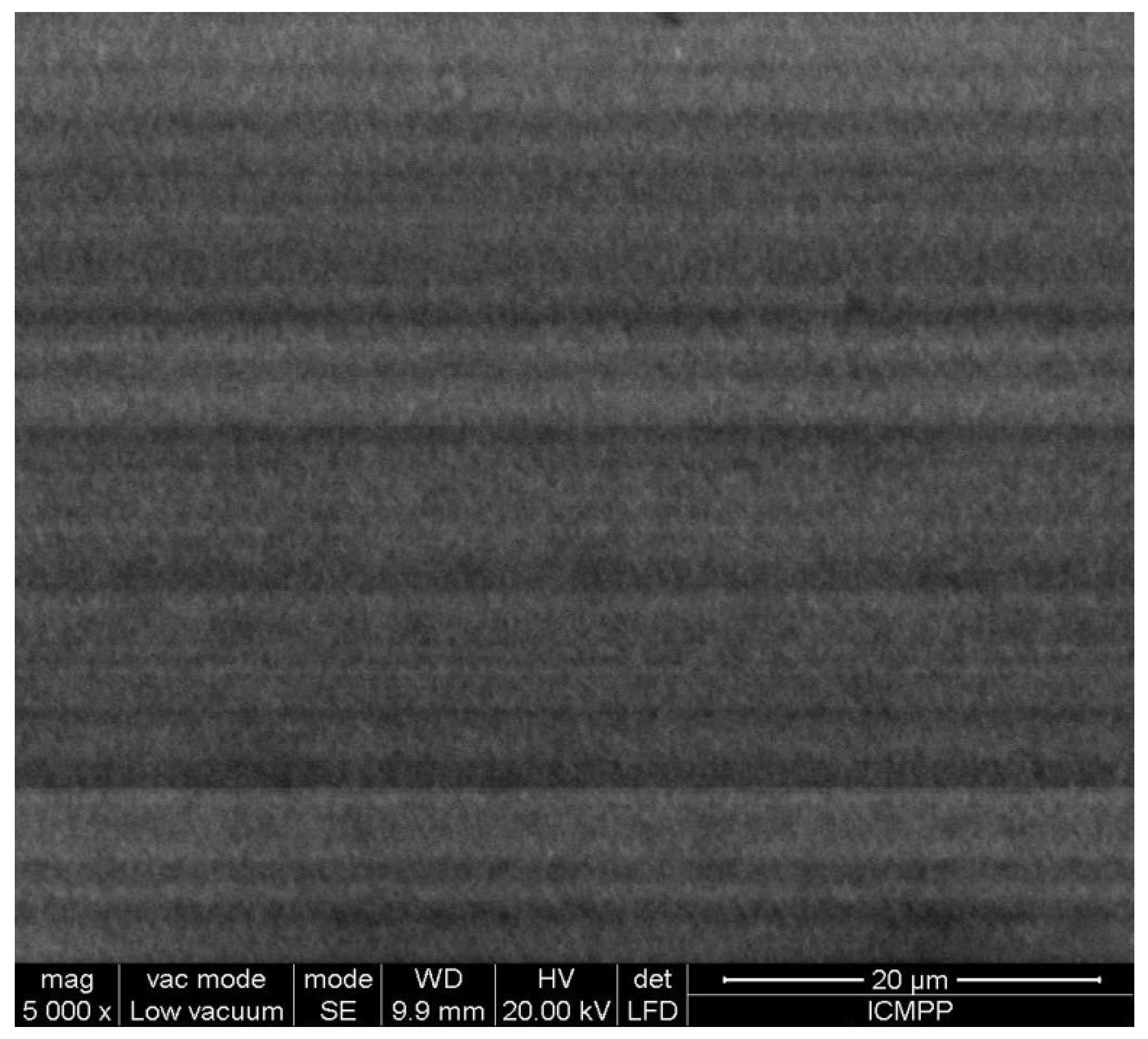
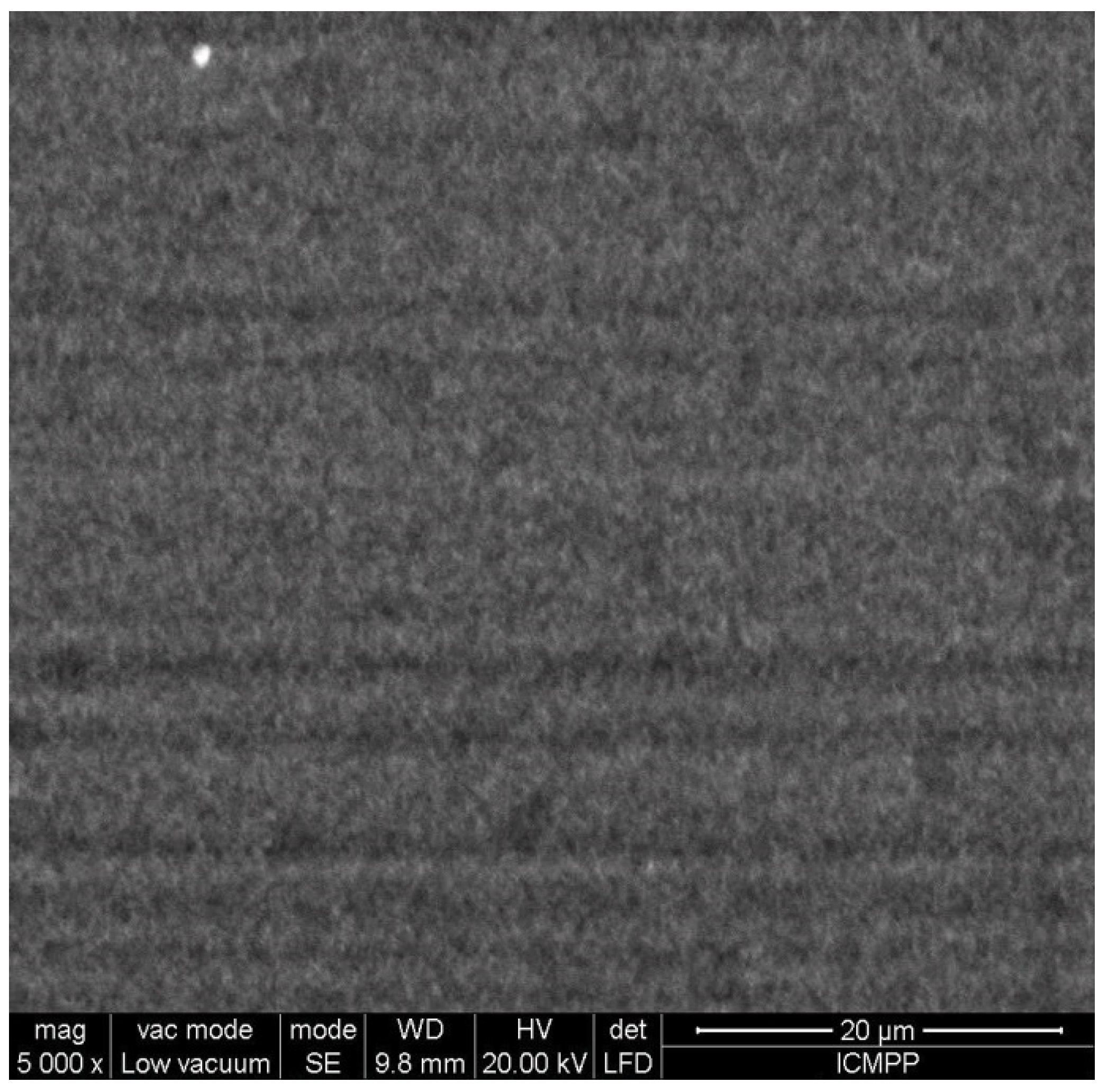
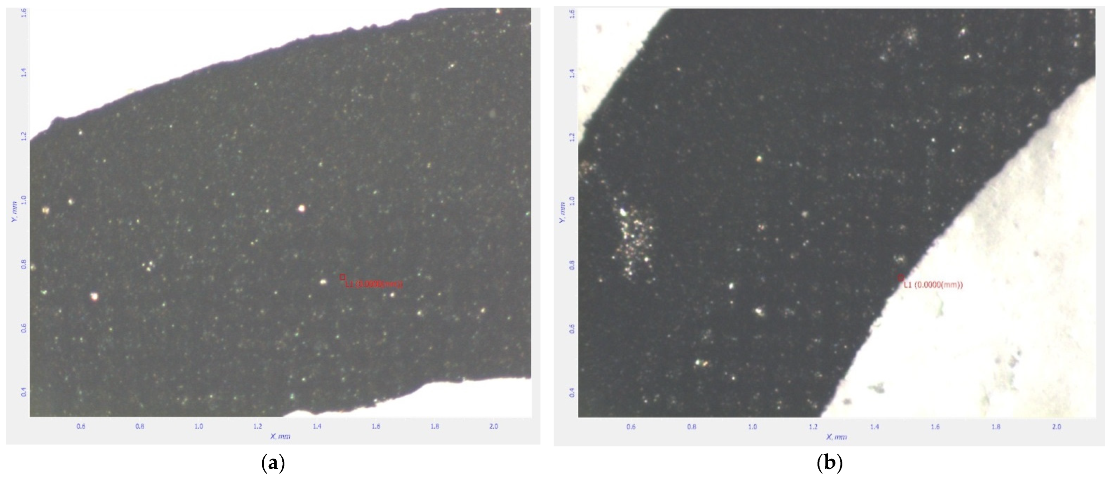
The diffractograms obtained upon the analyzed samples of ceramic nanotubes, before and after thermal exposure, are presented in Figure 5 for TiO2, Figure 6 for Al2O3 and Figure 7 for Y2O3. It can be observed that after thermal treatment is used to remove the organic material, the peaks in the diffractograms that appear before the heat treatment become more intense compared to the peaks that appear after, explained by the crystallization of the oxide materials during thermal exposure.
Thus, in Figure 5, the presence of a mixture of rutile and anatase phases specific to titanium dioxide can be observed. It can be noticed, after the heat treatment, the appearance of the characteristic maxima of the crystal planes (110) from 27° and (211) from 55°, specific to the rutile phase, as well as the crystal planes (101) from 25° and (200) from 48°, specific to the anatase phase of titanium dioxide.
In Figure 6, the existence of the amorphous phase before thermal treatment can be noticed by the presence in the diffractogram of the accentuated rise of the background only on the portion of 20–35° (not on the entire range of 2θ angles), a phenomenon that proves the existence of only some crystalline immature seeds and not an amorphous alumina in the true sense of the word.
In Figure 7, several diffraction maxima characteristic of yttrium oxide can be identified in both diffractograms, before and after thermal treatment, with the maxima at 29°, 34°, 49° and 58°.
The compositions of the samples before and after heat treatment were investigated using a scanning electron microscope. Thus, the analysis of the dispersed X-ray energies (EDX) of the samples of ceramic nanotubes are presented in Figure 8, Figure 9 and Figure 10.
In the case of the ceramic nanotubes obtained after thermal treatment, EDX analysis emphasized the presence of metallic elements such as Ti (18.53%), Al (13.03%) and Y (67.8%), along with O and Si from the ceramic support on which the nanotubes were deposited. On the other hand, some residual C (under 2%) can be noticed, maybe remnants from the thermal process, captured and stabilized among the crystals of the nanotubes.

SEM Analysis

The morphological analysis of the PMMA polymer nanofibers covered with ceramic materials and of the ceramic nanotubes, obtained after thermal treatment, was performed using a high-resolution scanning electron microscope. The SEM images of the structures are presented in Figure 11 for TiO2, Figure 12 for Al2O3, and Figure 13 for Y2O3.
In all cases, uniform dispersion of PMMA fibers within the deposited nets is noticed, with a uniform deposition of ceramic film upon PMMA fibers, as shown in Figure 11a, Figure 12a and Figure 13a. The nets maintained their dispersed and stable architecture after ceramic film deposition, due to the mechanical resistance assured by the optimal diameter of PMMA fibers.
Regarding the relative diameter of PMMA fibers covered with ceramic films, it is once again noticed that the dimensions are very close, between 0.5 and 0.6 μm, and the film deposition is quasi-uniform along the polymer fibers, as shown in Figure 11b, Figure 12b and Figure 13b, even if some vacancies can be noticed in the case of TiO2 and Y2O3, where the grains themselves have a more dispersed dimension at nano-scale. Finally, the images of ceramic nanotube before and after thermal process are relevant, as shown in Figure 11c, Figure 12c and Figure 13c, reconfirming once again the uniformity of ceramic nanotube structures, which are really empty inside.

3. Preparation of Specialized Inks for Screen-Printed Sensors

The research was conducted towards preparation of ceramic nanotubes containing inks in order to deposit them in the form of screen-printed electrodes on both ceramic and flexible supports. Due to the proven synergy between carbon nanotubes and ceramic nanostructures described in the literature, although with other applications, e.g., in [47,48,49,50], the developed screen-printing inks started from commercial inks containing carbon nanotubes, already tested for printed electronics, to which a defined quantity of ceramic nanotubes was added. A slight increase in ink viscosity has no relevance for the screen-printing process, because the commercial inks themselves present larger values of viscosity, even if they are dedicated to printing on a wide range of materials in general [51].

3.1. Preparation of Carbon Nanotubes Containing Ink with Ceramic Nanotubes

The experimental ink was prepared by uniformly dispersing tailored quantities of ceramic nanotubes in the commercial ink mass, under continuous stirring at approximately 100 rpm. The process and the ink image (after a classical dispersion using a small brush on a SiO support) are presented in Figure 14, where the ceramic nanotubes can be identified.
The preliminary ink properties are presented in Table 2.
An informal EDX microscopy analysis of ink after including the ceramic nanotubes (here TiO2 nanotubes) is presented in Figure 15, emphasizing the active nanotube content.

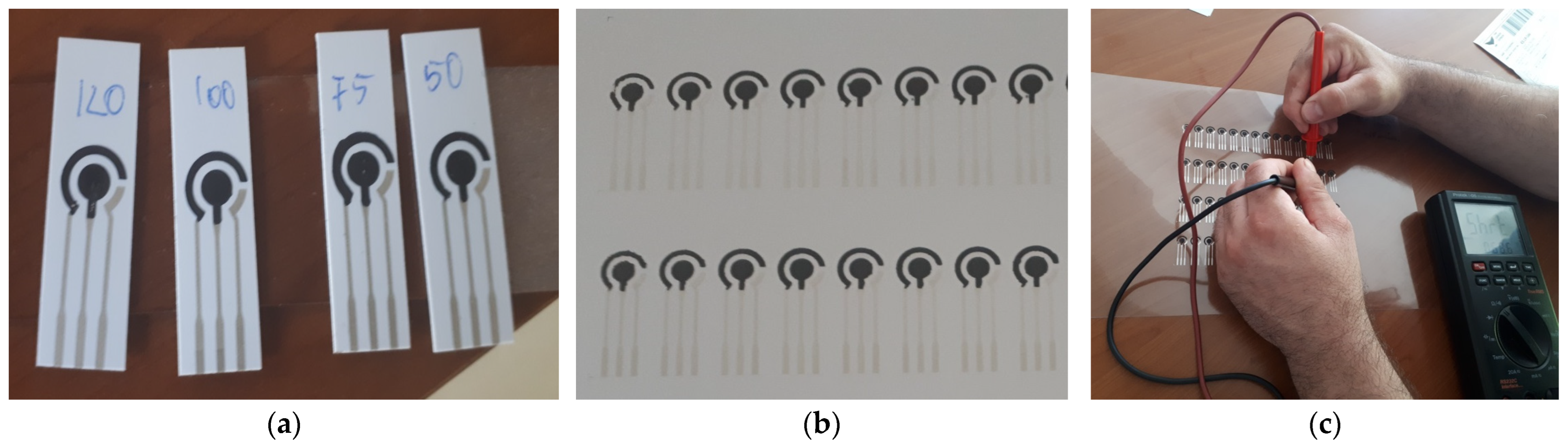
3.2. Experimental Printing and Testing Electrodes for a Classical Electrochemical Sensor

The conductive inks based on carbon and ceramic nanotubes were used for depositing the working electrode and the counter electrode of a classical electrochemical sensor (the connections are made with commercial silver-based inks).
The images of the experimental electrodes printed on the ceramic and polyethylene terephthalate (PET) supports are presented in Figure 16. The uniformity of the printing process can be noticed.

3.3. Results and Discussion

The SEM microscopy analysis of inks printed as experimental electrodes on PET are presented in Figure 17, Figure 18 and Figure 19.
It can be noticed that electrodes printed with inks containing TiO2 and Al2O3 nanotubes are more uniform, with lower roughness. The direction of screening can be also observed. As regards the electrodes printed with Y2O3 nanotubes, a higher roughness and some nonuniformity can be noticed, denoting the fact that these nanotubes are not mixing well with the carbon nanotubes within the experimental ink, and a specific additive should be tested in the future to increase the homogeneity of the ink.
The next step in printing technology with this experimental ink is related to the thermal maturation of printed electrodes. The commercial ink producer recommends for the ink with carbon nanotubes a maturation of up to 140 °C for maximum 10 min. We performed selective maturations from 50 °C to 120 °C (as seen in Figure 16a), but the comparative discussion was made for an exposure of 45 min at 75 °C, and of 15 min at 120 °C. In order to assess the curing of the experimental electrodes, both temperatures were taken into account, but the maturation process was assessed by the electrodes functionality, i.e., by testing their electrical resistance, measured with a precision ohmmeter, as in Figure 16. Informal images of the electrodes, after maturation at 75 °C and 120 °C, are presented in Figure 20 (here for the ink containing TiO2 nanotubes, ceramic support).
The darker color of the electrode maturated at 120 °C. The white dots are related to ceramic nanotube exposure.
A comparative analysis of the way the inks containing TiO2, Al2O3, and Y2O3, dried on the PET support after maturation at 120 °C is presented in Figure 21. The most uniform printed electrode route was achieved for the ink with Al2O3; in the rest, some minimal ink splashes can be observed. Printing on PET is more difficult compared to on the ceramic support, due to the tendency of the ink to spread due to the different surface tension. On the other hand, the plastic support suffers a visible thermal deformation at 120 °C. That is why it is recommended that the thermal process of curing should be longer—at lower temperatures for the plastic support, i.e., at 75 °C, even if the temperature can be kept at 120 °C for the ceramic support.
The final evaluation is related to electric resistance assessment at 1 cm length for each ink containing TiO2, Al2O3, and Y2O3, regardless of the support on which the electrode is placed. The experimental results are presented in Table 3, for electrode maturation at 75 °C and 120 °C. For comparison, the homologue resistance of the commercial carbon ink, used as a dispersion medium, was 3 Ω, in line with the values presented in Table 3, as explained by the low content of ceramic nanotubes. This is a very relevant aspect of printed electrodes, which benefit from the features of ceramic nanotubes without being detrimentally affected as regards their electrical parameters measured in direct current.
An increase in the conductivity of electrodes can be observed in the case of printed structures thermally treated at 120 °C, compared to 75 °C. This can be explained by the stronger connections of carbon nanotubes with ceramic nanotubes, with some modifications at contact surfaces, due to some specific reactions, which are now under a separate analysis. As regards their semiconducting properties and possible relation when interfering with carbon nanotubes, we can estimate that: TiO2 is a n-type semiconductor with a band gap of 3.2 eV, Al2O3 presents more insulating features, and Y2O3 may be assimilated with a semiconductor with a larger band gap of 5.5 eV, so the results of resistance are in line with the semiconducting features of each ceramic nanotube, i.e., the ink containing TiO2 leads to the lowest values of resistance. Even so, for practical application for printed sensors on flexible substrate, the difference is not so significant from an electronic point of view, so caution related to imposing a lower curing temperature for inks printed on the plastic support can be maintained.
In all, the experimental inks containing ceramic nanotubes can be considered feasible for printed electronics, because they offer fast curing at low temperatures, reasonable conductivity vs. electrode length, good printability on both ceramic or plastic (flexible) supports, good adhesion to surface after maturation (crosshatch adhesion of min. 4B) and minimal VOC exposure in electronic technology.
Further research will be dedicated to assessing the sensibility of such printed sensors in different chemical media and testing their features by using a potentiostat.

4. Conclusions

This paper describes the process to obtain ceramic nanotubes from titanium, aluminum and yttrium oxides by a feasible, replicable and reliable technology, including three stages: preliminary manufacture of polymer fibers nets of poly(methyl methacrylate) from a solution of 10 wt%, with dimethylformamide (DMF) as solvent; magnetron deposition of ceramic films upon PMMA nanofibers nets; thermal treatment of nanotubes at 600 °C for a complete combustion of PMMA support.
The best results for PMMA nanofibers nets were obtained by using a 10% PMMA solution at voltages of 20 kV, with a drum rotation speed of 5 rpm, because the fiber nets were more homogenous in spatial deposition, and also more homogenous in diameter. A minimum diameter of 0.3 μm was consider optimal for PMMA nanofibers in order to maintain the structural stability of covered fibers, from a mechanical point of view. After ceramic film deposition, the PMMA net structure leads to a fiber diameter of 0.5–0.6 μm.
After chemical–physical analyses of stages towards obtaining ceramic nanotubes, uniform dispersion of PMMA fibers within the deposited nets, with uniform deposition of ceramic film upon PMMA fibers, was noticed. Finally, images of ceramic nanotubes before and after thermal process were presented, reconfirming the uniformity of the ceramic nanotube structures, which are empty inside.
The technological purpose was to use such nanotubes as ingredients in screen-printing inks dedicated to printed electronics, with further target on innovative nano-sensor development, because no study directly targeted the subject of ceramic nanotube applications for printed electronics to date. Due to the proven synergy between carbon nanotubes and ceramic nanostructures, the developed screen-printing inks started from commercial inks containing carbon nanotubes, already tested for printed electronics, to which a defined quantity of ceramic nanotubes was added. The physical parameters of the new inks were as follows: solids content 48%; density 2 g/mL; viscosity at 10 s−1 6500; pH 6. Uniform dispersion of ceramic nanotubes within the inks was demonstrated. The conductive inks based on carbon and ceramic nanotubes were used for depositing the working electrode and the counter electrode of a classical electrochemical sensor (the connections are made with commercial silver-based inks).
Electrodes printed with inks containing TiO2 and Al2O3 nanotubes were more uniform, with lower roughness. After thermal curing of the electrodes, it was noticed that the most uniform printed electrodes were achieved for the ink with Al2O3; in the rest, some minimal ink splashes can be observed. Printing on PET is more difficult compared to on the ceramic support, due to the tendency of the ink to spread due to the different surface tension. On the other hand, the thermal process should be longer—at lower temperatures for the plastic support, because it may suffer thermal deformations.
A significant increase in the conductivity of electrodes can be observed in the case of electrodes thermally treated at 120 °C, compared to 75 °C, with at least 40%. This can be explained by the stronger connections of carbon nanotubes with ceramic nanotubes, with some modifications at contact surfaces, due to some specific reactions, to be further investigated.
The experimental inks containing ceramic nanotubes can be considered feasible for printed electronics, because they offer fast curing at low temperatures, reasonable conductivity vs. electrode length, good printability on both ceramic or plastic (flexible) supports and good adhesion to surface after maturation.

Author Contributions

Conceptualization, A.F.T. and R.C.C.; methodology, R.C.C., O.D.S., M.A. and A.F.T.; validation, R.C.C., O.D.S. and A.F.T.; formal analysis, A.F.T., S.T.A., M.A. and O.D.S.; investigation, R.C.C., O.D.S., A.F.T., M.A. and S.T.A.; data curation, R.C.C., O.D.S., M.A. and A.F.T.; writing—original draft preparation, A.F.T. and R.C.C.; writing—review and editing, R.C.C. and A.F.T.; visualization, R.C.C. and A.F.T.; supervision, A.F.T. and R.C.C. All authors have read and agreed to the published version of the manuscript.

Funding

This research received no external funding.

Data Availability Statement

The data presented in this study are available on request from the corresponding author.

Conflicts of Interest

The authors declare no conflict of interest.

References

  1. Balhaddad, A.A.; Garcia, I.M.; Mokeem, L.; Alsahafi, R.; Collares, F.M.; Sampaio de Melo, M.A. Metal Oxide Nanoparticles and Nanotubes: Ultrasmall Nanostructures to Engineer Antibacterial and Improved Dental Adhesives and Composites. Bioengineering 2021, 8, 146. [Google Scholar] [CrossRef] [PubMed]
  2. Lee, M.; Kim, T.; Bae, C.; Shin, H.; Kim, J. Fabrication and applications of metal-oxide nano-tubes. JOM J. Miner. Met. Mater. Soc. 2010, 62, 44–49. [Google Scholar] [CrossRef]
  3. Researchers Learn to Control the Dimensions of Metal Oxide Nanotubes. Available online: https://phys.org/news/2007-08-dimensions-metal-oxide-nanotubes.html (accessed on 10 March 2024).
  4. Enculescu, M.; Costas, A.; Evanghelidis, A.; Enculescu, I. Fabrication of ZnO and TiO2 Nanotubes via Flexible Electro-Spun Nanofibers for Photocatalytic Applications. Nanomaterials 2021, 11, 1305. [Google Scholar] [CrossRef]
  5. Ramasamy, P.; Lim, D.H.; Kim, J.; Kim, J. A general approach for synthesis of functional metal oxide nanotubes and their application in dye-sensitized solar cells. RSC Adv. 2014, 4, 2858–2864. [Google Scholar] [CrossRef]
  6. Li, D.; McCann, J.T.; Xia, Y.; Marquez, M. Electrospinning: A Simple and Versatile Technique for Producing Ceramic Nanofibers and Nanotubes. J. Am. Ceram. Soc. 2006, 89, 1861–1869. [Google Scholar] [CrossRef]
  7. Li, Y.; Yang, X.Y.; Feng, Y.; Yuan, Z.Y.; Su, B.L. One-Dimensional Metal Oxide Nanotubes, Nanowires, Nanoribbons, and Nanorods: Synthesis, Characterizations, Properties and Applications. Crit. Rev. Solid State Mater. Sci. 2012, 37, 1–74. [Google Scholar] [CrossRef]
  8. Azevedo, J.; Fernández-García, M.P.; Magén, C.; Mendes, A.; Araújo, J.P.; Sousa, C.T. Double-walled iron oxide nanotubes via selective chemical etching and Kirkendall process. Sci. Rep. 2019, 9, 11994. [Google Scholar] [CrossRef] [PubMed]
  9. Parthangal, P. Direct synthesis of tin oxide nanotubes on microhotplates using carbon nanotubes as templates. J. Mater. Res. 2011, 26, 430–436. [Google Scholar] [CrossRef]
  10. Falk, M.; Luwan, S.; Tintula, K.; Markus, A.; Sandra, S.; Ulrike, K.; Molina-Luna, L.; Duerrschnabel, M.; Kleebe, H.J.; Ayata, S.; et al. Free-Standing Networks of Core–Shell Metal and Metal Oxide Nanotubes for Glucose Sensing. ACS Appl. Mater. Interfaces 2017, 9, 771–781. [Google Scholar]
  11. Kang, D.Y. Single-Walled Metal Oxide Nanotubes and Nanotube Membranes for Molecular Separations (Thesis). 2012. Available online: https://core.ac.uk/reader/10189860 (accessed on 10 March 2024).
  12. Muto, H.; Sato, Y.; Tan, W.K.; Yokoi, A.; Kawamura, G.; Matsuda, A. Controlled formation of carbon nanotubes incorporated ceramic composite granules by electrostatic integrated nano-assembly. Nanoscale 2022, 14, 9669–9674. [Google Scholar] [CrossRef]
  13. Mallakpour, S.; Khadem, E. Carbon nanotube–metal oxide nanocomposites: Fabrication, properties and applications. Chem. Eng. J. 2016, 302, 344–367. [Google Scholar] [CrossRef]
  14. Rahat, S.S.M.; Hasan, K.M.Z.; Mondol, M.M.H.; Mallik, A.K. A comprehensive review of carbon nanotube-based metal oxide nanocomposites for supercapacitors. J. Energy Storage 2023, 73, 108847. [Google Scholar] [CrossRef]
  15. Gupta, V.; Saleh, T. Syntheses of Carbon Nanotube-Metal Oxides Composites; Adsorption and Photo-Degradation, Volume: Carbon Nanotubes-From Research to Applications. 2011. Available online: https://www.intechopen.com/chapters/16834 (accessed on 10 March 2024). [CrossRef]
  16. Wang, D.; Sun, W.; Su, C. Carbon Nanotube–Metal Oxide Nanocomposites. In Metal Oxide Nanocomposites: Synthesis and Applications; Scrivener Publishing LLC: Austin, TX, USA, 2020; Chapter 4. [Google Scholar] [CrossRef]
  17. Saboor, F.H.; Ataei, A. Decoration of Metal Nanoparticles and Metal Oxide Nanoparticles on Carbon Nanotubes. Adv. J. Chem. 2024, 7, 122–145. [Google Scholar] [CrossRef]
  18. Kumar, N.; Navani, N.K.; Manhas, S.K. Effect of Metal Oxide Nanoparticles on Carbon Nanotube Device Characteristics. J. Electron. Mater. 2021, 50, 528–536. [Google Scholar] [CrossRef]
  19. Available online: https://eureka.patsnap.com/patent-CN103058173B (accessed on 10 March 2024).
  20. Cho, H.H.; Smith, B.A.; Wnuk, J.D.; Fairbrother, D.H.; Ball, W.P. Influence of Surface Oxides on the Adsorption of Naphthalene onto Multiwalled Carbon Nanotubes. Environ. Sci. Technol. 2008, 42, 2899–2905. [Google Scholar] [CrossRef] [PubMed]
  21. Elkady, M.F.; Hassan, H.S.; Amer, W.A.; Salama, E.; Algarni, H.; Shaaban, E.R. Novel Magnetic Zinc Oxide Nanotubes for Phenol Adsorption: Mechanism Modeling. Materials 2017, 10, 1355. [Google Scholar] [CrossRef]
  22. Ali, M.A.; Solanki, P.R.; Srivastava, S.; Singh, S.; Agrawal, V.V.; John, R.; Malhotra, B.D. Protein Functionalized Carbon Nanotubes-based Smart Lab-on-a-Chip. ACS Appl. Mater. Interfaces 2015, 7, 5837–5846. [Google Scholar] [CrossRef] [PubMed]
  23. Wang, H.; Boghossian, A. Covalent conjugation of proteins onto fluorescent single-walled carbon nanotubes for biological and medical applications. Mater. Adv. 2023, 4, 823–834. [Google Scholar] [CrossRef]
  24. Hohman, M.; Shin, M.; Rutledge, G.; Brenner, M. Electrospinning and electrically forced jets. II. Applications. Phys. Fluids 2021, 13, 2221–2236. [Google Scholar] [CrossRef]
  25. Zuo, W.; Zhu, M.; Yang, W.; Yu, H.; Chen, Y.; Zhang, Y. Experimental study on relationship between jet instability and formation of beaded fibers during electrospinning. Polym. Eng. Sci. 2005, 45, 704–709. [Google Scholar] [CrossRef]
  26. Fridrikh, S.V.; Yu, J.H.; Brenner, M.P.; Rutledge, G.C. Controlling the Fiber Diameter during Electrospinning. Phys. Rev. Lett. 2003, 90, 144502. [Google Scholar] [CrossRef] [PubMed]
  27. Tao, J.; Shivkumar, S. Molecular weight dependent structural regimes during the electrospinning of PVA. Mater. Lett. 2007, 61, 2325–2328. [Google Scholar] [CrossRef]
  28. Oleiwi, A.; Jabur, A.; Alsalhy, Q. Preparation of Polystyrene/Polyacrylonitrile Blends by Electrospinning Technique. J. Phys. Conf. Ser. 2021, 1879, 022065. [Google Scholar] [CrossRef]
  29. Kim, H.; Kim, W.; Jin, H.J.; Chin, I.J. Morphological Characterization of Electrospun Nano-Fibrous Membranes of Biodegradable Poly(L-lactide) and Poly(lactide-co-glycolide). Macromol. Symp. 2005, 224, 145–154. [Google Scholar] [CrossRef]
  30. Nezarati, R.; Eifert, M.; Cosgriff-Hernandez, E. Effects of Humidity and Solution Viscosity on Electrospun Fiber Morphology. Tissue Eng. Part C Methods 2013, 19, 810–819. [Google Scholar] [CrossRef] [PubMed]
  31. Wang, X.; Sun, M.; Murugananthan, M.; Zhang, Y.; Zhang, L. Electrochemically self-doped WO3/TiO2 nanotubes for photocatalytic degradation of volatile organic compounds. Appl. Catal. B Environ. 2020, 260, 118205. [Google Scholar] [CrossRef]
  32. Kéri, O.; Kocsis, E.; Karajz, D.A.; Nagy, Z.K.; Parditka, B.; Erdélyi, Z.; Szabó, A.; Hernádi, K.; Szilágyi, I.M. Photocatalytic Crystalline and Amorphous TiO2 Nanotubes Prepared by Electrospinning and Atomic Layer Deposition. Molecules 2021, 26, 5917. [Google Scholar] [CrossRef] [PubMed]
  33. Stoilova, O.; Manolova, N.; Rashkov, I. Electrospun Poly(methyl methacrylate)/TiO2 Composites for Photocatalytic Water Treatment. Polymers 2021, 13, 3923. [Google Scholar] [CrossRef] [PubMed]
  34. Chawraba, K.; Damiri, F.; Toufaily, J.; Lalevee, J.; Hamieh, T. TiO2 Supported in Polymethyl methacrylate (PMMA) Properties, Preparation, and Photocatalytic Activity for the Degradation of Synthetic Dyes. Lett. Appl. NanoBioSci. 2024, 13, 13. [Google Scholar] [CrossRef]
  35. Ounas, O.; El Foulani, A.; Lekhlif, B.; Jamal-Eddine, J. Immobilization of TiO2 into a poly methyl methacrylate (PMMA) as hybrid film for photocatalytic degradation of methylene blue. Mater. Today Proc. 2020, 22, 35–40. [Google Scholar] [CrossRef]
  36. Baji, A.; Mai, Y.W. Engineering Ceramic Fiber Nanostructures Through Polymer-Mediated Electrospinning, Volume: Polymer-Engineered Nanostructures for Advanced Energy Applications. 2017, pp. 3–30. Available online: https://link.springer.com/chapter/10.1007/978-3-319-57003-7_1 (accessed on 10 March 2024).
  37. Mafakheri, E.; Salimi, A.; Hallaj, R.; Ramazani, A.; Kashi, M.A. Synthesis of Iridium Oxide Nanotubes by Electrodeposition into Polycarbonate Template: Fabrication of Chromium(III) and Arsenic(III) Electrochemical Sensor. Electroanalysis 2011, 23, 2429–2437. [Google Scholar] [CrossRef]
  38. Lim, J.H.; Min, S.G.; Malkinskib, L.; Wiley, J. Iron oxide nanotubes synthesized via template-based electrodeposition. Nanoscale 2014, 6, 5289–5295. [Google Scholar] [CrossRef] [PubMed]
  39. Alkanad, K.; Hezam, A.; Al-Zaqri, N.; Bajiri, M.A.; Alnaggar, G.; Drmosh, Q.A.; Almukhlifi, H.A.; Neratur Krishnappagowda, L. One-Step Hydrothermal Synthesis of Anatase TiO2 Nanotubes for Efficient Photocatalytic CO2 Reduction. ACS Omega 2022, 7, 38686–38699. [Google Scholar] [CrossRef] [PubMed]
  40. Nakahira, A.; Kubo, T.; Numako, C. Formation Mechanism of TiO2-Derived Titanate Nanotubes Prepared by the Hydrothermal Process. Inorg. Chem. 2010, 49, 5845–5852. [Google Scholar] [CrossRef]
  41. Gao, H.; Tang, X.; Zhang, H.; He, Y.; Zhou, T.; Shen, J.; Zhu, L.; Si, T. Mechanical strength enhancement of CaZr4P6O24 ceramics with multi-walled carbon nanotubes additions. J. Alloys Compd. 2024, 976, 173310. [Google Scholar] [CrossRef]
  42. Porras, R.; Bavykin, D.V.; Zekonyte, J.; Walsh, F.C.; Wood, R.J. Titanate nanotubes for reinforcement of a poly(ethylene oxide)/chitosan polymer matrix. Nanotechnology 2016, 27, 195706. [Google Scholar] [CrossRef]
  43. Hedayati, M.; Taheri-Nassaj, E.; Yourdkhani, A.; Borlaf, M.; Zhang, J.; Calame, M.; Sebastian, T.; Payandeh, S.; Clemens, F.J. BaTiO3 nanotubes by co-axial electrospinning: Rheological and microstructural investigations. J. Eur. Ceram. Soc. 2020, 40, 1269–1279. [Google Scholar] [CrossRef]
  44. Lin, Z.; Yang, Y.; Zhang, A. (Eds.) Engineering Ceramic Fiber Nanostructures Through Polymer-Mediated Electrospinning. In Polymer-Engineered Nanostructures for Advanced Energy Applications; Springer: Berlin/Heidelberg, Germany, 2017; Volume 3. [Google Scholar] [CrossRef]
  45. Moreno, M.; Arredondo, M.; Ramasse, Q.M.; McLaren, M.; Stötzner, P.; Förster, S.; Benavente, E.; Salgado, C.; Devis, S.; Solar, P.; et al. ZnO nucleation into trititanate nanotubes by ALD equipment techniques, a new way to functionalize layered metal oxides. Sci. Rep. 2021, 11, 7698. [Google Scholar] [CrossRef]
  46. Karacaoglu, E.; Öztürk, E.; Uyaner, M.; Losego, M.D. Atomic layer deposition (ALD) of nanoscale coatings on SrAl2O4-based phosphor powders to prevent aqueous degradation. J. Am. Ceram. Soc. 2020, 103, 3706–3715. [Google Scholar] [CrossRef]
  47. Liu, H.; Takagi, D.; Ohno, H.; Chiashi, S.; Chokan, T.; Homma, Y. Growth of Single-Walled Carbon Nanotubes from Ceramic Particles by Alcohol Chemical Vapor Deposition. Appl. Phys. Express 2008, 1, 014001. [Google Scholar] [CrossRef]
  48. Lamnini, S.; Pugliese, D.; Baino, F. Zirconia-Based Ceramics Reinforced by Carbon Nanotubes: A Review with Emphasis on Mechanical Properties. Ceramics 2023, 6, 1705–1734. [Google Scholar] [CrossRef]
  49. Marinho, T.; Costa, P.; Lizundia, E.; Costa, C.M.; Corona-Galván, S.; Lanceros-Méndez, S. Ceramic Nanoparticles and Carbon Nanotubes Reinforced Thermoplastic Materials for Piezocapacitive Sensing Applications’. Available online: https://repositorium.uminho.pt/bitstream/1822/64639/1/37.pdf (accessed on 10 March 2024).
  50. Single-Walled Carbon Nanotube-Ceramic Composites and Methods of Use (Patent). Available online: https://patents.google.com/patent/AU2004234395A1/en (accessed on 10 March 2024).
  51. Chu, Z.; Peng, J.; Jin, W. Advanced nanomaterial inks for screen-printed chemical sensors. Sens. Actuators B Chem. 2017, 243, 919–926. [Google Scholar] [CrossRef]
Figure 1. PMMA nanofibers net deposited at 12 kV.
Crystals 14 00454 g001
Figure 2. PMMA nanofibers net deposited at 15 kV.
Crystals 14 00454 g002
Figure 3. PMMA nanofibers net deposited at 20 kV.
Crystals 14 00454 g003
Figure 4. Dimensions of nanofibers before (a) and after (b) ceramic film deposition.
Crystals 14 00454 g004
Figure 5. Diffractogram for TiO2 ceramic nanotubes.
Crystals 14 00454 g005
Figure 6. Diffractogram for Al2O3 ceramic nanotubes.
Crystals 14 00454 g006
Figure 7. Diffractogram for Y2O3 ceramic nanotubes.
Crystals 14 00454 g007
Figure 8. EDX results for TiO2 ceramic nanotubes.
Crystals 14 00454 g008
Figure 9. EDX results for Al2O3 ceramic nanotubes.
Crystals 14 00454 g009
Figure 10. EDX results for Y2O3 ceramic nanotubes.
Crystals 14 00454 g010
Figure 11. SEM images for TiO2 ceramic nanotubes technology: (a) PMMA net with TiO2 ceramic film (500 magnitude, selected area); (b) PMMA nanofiber with TiO2 ceramic cover; (c) TiO2 ceramic nanotube before and after thermal process (100 k magnitude, with image processing).
Crystals 14 00454 g011
Figure 12. SEM images for Al2O3 ceramic nanotubes technology: (a) PMMA net with Al2O3 ceramic film (500 magnitude, selected area); (b) PMMA nanofiber with Al2O3 ceramic cover; (c) Al2O3 ceramic nanotube before and after thermal process (100 k magnitude, with image processing).
Crystals 14 00454 g012
Figure 13. SEM images for Y2O3 ceramic nanotubes technology: (a) PMMA net with Y2O3 ceramic film (500 magnitude, selected area); (b) PMMA nanofiber with Y2O3 ceramic cover; (c) Y2O3 ceramic nanotube before and after thermal process (100 k magnitude, with image processing).
Crystals 14 00454 g013
Figure 14. Preparation of experimental ink and image of the ink deposition.
Crystals 14 00454 g014
Figure 15. EDX analysis of the experimental ink.
Crystals 14 00454 g015
Figure 16. Experimental electrodes printed on (a) ceramic and (b) PET supports; (c) resistance measurements.
Crystals 14 00454 g016
Figure 17. SEM images for the printed electrode with ink containing TiO2 nanotubes.
Crystals 14 00454 g017
Figure 18. SEM images for the printed electrode with ink containing Al2O3 nanotubes.
Crystals 14 00454 g018
Figure 19. SEM images for the printed electrode with ink containing Y2O3 nanotubes.
Crystals 14 00454 g019
Figure 20. Images of the printed electrodes containing TiO2 nanotubes, after maturation at (a) 75 °C, and (b) 120 °C.
Crystals 14 00454 g020
Figure 21. Images of the printed electrodes of containing (a) TiO2, (b) Al2O3, and (c) Y2O3 nanotubes, all after maturation at 120 °C.
Crystals 14 00454 g021
Table 1. Experimental plan for electrospinning process.
SamplePMMA (%)U (kV)Distance (mm)Rotation Speed (rpm)
11012100-
21015100-
31020100-
4102080-
51015805
61012805
7512805
8515805
9520805
105201005
115151005
125121005
Table 2. Experimental ink features.
Characteristic Value [+/− 5%]
Solids content [wt. %]48
Density [g/mL]2
Viscosity at 10 s−16500
pH6
Table 3. Electric resistance of electrodes at 1 cm length.
Resistance [Ω]Ink Containing TiO2Ink Containing Al2O3Ink Containing Y2O3
75 °C5.47.26.8
120 °C3.23.43.6
Disclaimer/Publisher’s Note: The statements, opinions and data contained in all publications are solely those of the individual author(s) and contributor(s) and not of MDPI and/or the editor(s). MDPI and/or the editor(s) disclaim responsibility for any injury to people or property resulting from any ideas, methods, instructions or products referred to in the content.

