Article

Ultrahigh Responsivity In2O3 UVA Photodetector through Modulation of Trimethylindium Flow Rate

1
State Key Laboratory of High-Power Semiconductor Laser, School of Physics, Changchun University of Science and Technology, Changchun 130022, China
2
A Nanofabrication Facility, Suzhou Institute of Nano-Tech and Nano-Bionics, Chinese Academy of Sciences, Suzhou 215123, China
3
School of Nano Technology and Nano Bionics, University of Science and Technology of China, Hefei 230026, China
*
Authors to whom correspondence should be addressed.
Crystals 2024, 14(6), 494; https://doi.org/10.3390/cryst14060494
Submission received: 20 April 2024 / Revised: 20 May 2024 / Accepted: 21 May 2024 / Published: 24 May 2024

Abstract

:
Oxygen vacancies (Vo) can significantly degrade the electrical properties of indium oxide (In2O3) thin films, thus limiting their application in the field of ultraviolet detection. In this work, the Vo is effectively suppressed by adjusting the Trimethylindium (TMIn) flow rate (fTMIn). In addition, with the reduction of the fTMIn, the background carrier concentration and the roughness of the film decrease gradually. And a smooth In2O3 thin film with roughness of 0.44 nm is obtained when the fTMIn is 5 sccm. The MSM photodetectors (PDs) are constructed based on In2O3 thin films with different fTMIn to investigate the opto-electric characteristics of the films. The dark current of the PDs is significantly reduced by five orders from 100 mA to 0.28 μA with the reduction of the fTMIn from 50 sccm to 5 sccm. In addition, the photo response capacity of PDs is dramatically enhanced. The photo-to-dark current ratio (PDCR) increases from 0 to 2589. Finally, the PD with the fTMIn of 5 sccm possesses a record-high responsivity of 2.53 × 10³ AW−1, a high detectivity of 5.43 × 10⁷ Jones and a high EQE of 9383 × 100%. Our work provides an important reference for the fabrication of high-sensitivity UV PDs.

1. Introduction

Ultraviolet-A (UVA) photodetectors (PDs) have attracted wide attention in both civilian and military applications, such as flame detection, ultraviolet cameras, and missile early warning systems [1,2,3,4,5,6,7,8,9]. Indium compounds such as In2Se3, In2S3 and In2O3 are widely reported for efficient photoelectric detection [10,11,12,13,14,15,16,17,18]. Because metal oxides can be used as interface layers in metal/semiconductor contacts to change the optoelectronic properties of heterojunctions, they are widely used in optoelectronic devices [19]. Therefore, In2O3 has been considered a promising candidate for UVA PD fabrication among indium compounds, due to its suitable bandgap (3.7 eV), high mobility and stable chemical and optical properties [20,21,22]. Currently, UVA PDs based on In2O3 thin films mainly depends on the photovoltaic effect, because it can realize the efficient separation and collection of photogenerated carriers through the built-in electric field and reduce the dark current of the device [23,24,25]. The device structure based on photovoltaic effect mainly includes heterojunctions, transistors and metal–semiconductor–metal (MSM) structures. Among these, MSM PDs offer competitive advantages such as simple structure, ease of fabrication and convenient circuit integration [26].
In2O3 MSM PDs are typically integrated with circuits through flip-chip bonding, enabling their application in UV imaging via back illumination. Therefore, low-cost and UVA-transparent sapphire substrates are widely used for In2O3 thin film detectors. In addition, the epitaxy of high-crystal-quality In2O3 thin films has been reported through HVPE, MBE and MOCVD. Due to its ability to produce high-uniform and reproducible thin films, MOCVD offers advantages such as rapid growth rates that enhance production efficiency and reduce costs for the commercialization of high-quality In2O3 thin films and their detectors. However, defects such as oxygen vacancies (Vo) in the In2O3 thin film can deteriorate the performance of the PDs, which significantly limits their application [27]. It has been reported that the Vo has a significant effect on the metal/semiconductor interface and leads to a decrease in the Schottky barrier, resulting in a significant increase in the dark current of the detector [28]. In addition, the ionized oxygen vacancy can capture photogenerated electrons, and the release process is very slow after the light source is turned off, resulting in a persistent photoconductive effect and degradation of the response speed [29]. Ge et al. proposed hydrogen (H) doping in In2O3 through magnetron sputtering and proved H can occupy the Vo [30]. With the H doping concentration of 1%, the thin film showed a high mobility of 115.3 cm2 V−1s−1. However, H exhibits low stability in In2O3 thin films and tends to escape at high temperatures.
In this work, we significantly suppress the defects of Vo in In2O3 thin films by adjusting the Trimethylindium (TMIn) flow rate (fTMIn) during film growth. With a reduction in the fTMIn, not only the concentration of Vo is suppressed, but also the performance of the In2O3 PDs is improved. Consequently, the dark current of the PDs based on the In2O3 thin film decreased by five magnitudes. In addition, the UV PD exhibits a high responsivity (2.53 × 10³ AW−1) and a high detectivity (5.43 × 10⁷ Jones). This work provides an important reference for the fabrication of high-performance UVA PDs based on In2O3 thin film.

2. Materials and Methods
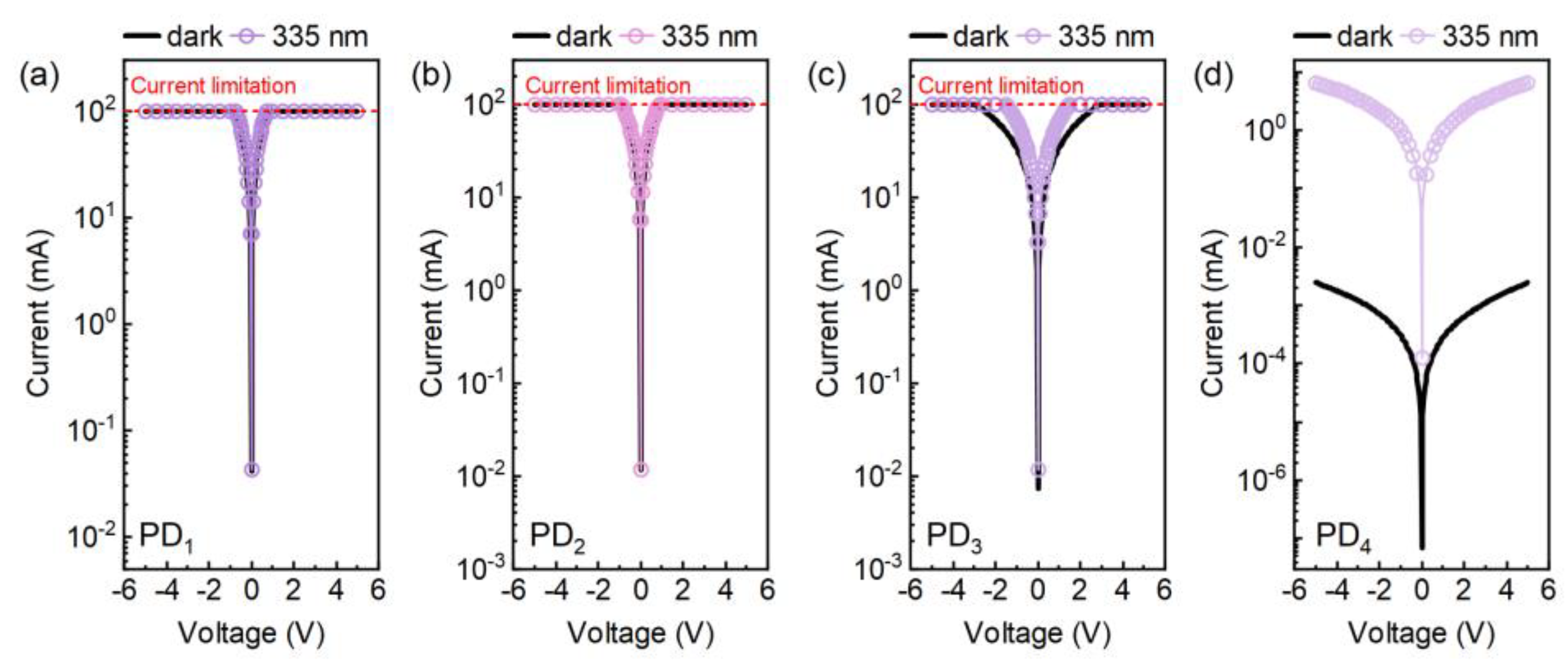
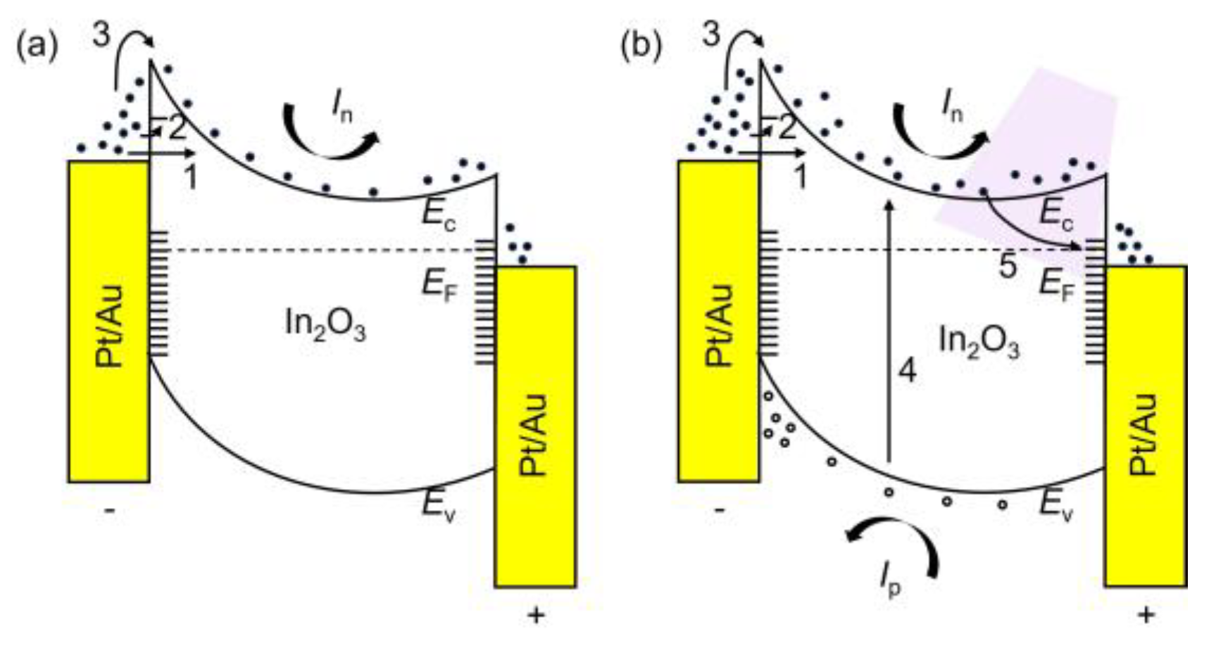
The unintentionally doped (UID) In2O3 thin films are grown on sapphire substrates using MOCVD. The growth is performed at 600 °C for 120 min. TMIn is used as the In precursor and the flow rate of O2 (99.999%) is fixed at 1000 sccm. High-purity nitrogen (N2) serves as the carrier gas. To construct a UVA PD, the Pt/Au (50/100 nm) bilayer metal is deposited on the In2O3 thin film by electron beam evaporation. Finally, the electrodes are patterned into intercalated fingers with a length of 480 μm, a width of 10 μm and a spacing of 10 μm. The electrodes contain 12 pairs of fingers, and the area of the active region is 1.3 × 10⁻³ cm2.
The thickness of the In2O3 thin films is measured to be approximately 50 nm using SEM as shown in Figure S1 in Supplementary Materials. The crystal structure and crystallinity of In2O3 thin films are characterized by X-ray diffraction (XRD) with a test voltage of 40 kV, a current of 40 mA and a step size of 0.02°/s The chemical compositions of the In2O3 thin films are analyzed by X-ray photoelectron spectroscopy (XPS). An XPS instrument with a base pressure better than 4.4 × 10⁻⁸ Pa is used to acquire core-level XPS spectra from the sample. Monochromatic Al Kα radiation source (hv = 1486.6 eV) is employed. The size of analyzed area is 100 × 100 μm and the optoelectronic detection angle was 45°. Argon ion etching is not carried out to avoid the influence of etching damage on the atomic ratio [31]. The surface morphologies are obtained by atomic force microscopy (AFM) with am amplitude of 200~300 mV and a scanning speed of 1 Hz. The carrier concentration and mobility are tested by Hall measurements. The optoelectronic performance of the devices is measured via a probe station equipped with Keysight B1505A (Colorado Springs, United States), and a commercial monochromatic tunable light sources system (Omno150300, Abuja, NigeriaNBET), including Xenon lamp, Monochromator, chopper and optical fibers.

3. Results

The In2O3 thin films grown at the fTMIn of 50, 25, 10 and 5 sccm are labeled as S1, S2, S3 and S4, respectively. In order to study the effect of fTMIn on the crystal structure and crystallinity of the In2O3 thin films, XRD measurements are carried out. As shown in Figure 1a, the diffraction peak observed near 41.68° corresponds to the (0006) plane of the sapphire substrate. In addition, two diffraction peaks located at 30.65° and 64° are observed, which correspond to the (222) and (444) planes of In2O3. The results indicate that the heteroepitaxial In2O3 thin films grown on c-plane sapphire have a preferred orientation along the (222) direction. The coherent volume of specific diffraction peaks in thin films is related to the size of crystallite [32]. According to Scherrer’s relation, the size of the crystallites in S1 to S4 can be calculated using the following equation:
Crystallite   size   ( D ) = 0.9 λ β c o s   θ
where λ = 1.54 Å is the wavelength of the Cu Kα line, θ is the Bragg’s angle and β is the full width at half maximum (FWHM). Therefore, the D of S1 to S4 can be calculated to be 28.0 nm, 15.9 nm, 7.4 nm and 4.3 nm, respectively. In addition, the dislocation density can be expressed as
Dislocation   density   ( δ ) = 1 D 2
According to Equation (2), the δ of S1 to S4 can be estimated to be 1.27 × 1011 cm−2, 3.95 × 1011 cm−2, 1.83 × 1012 cm−2 and 5.53 × 1012 cm−2, respectively. The size of the crystallites has a significant influence on the crystallite number (NC). The NC can be estimated using the following equation:
N C = d D 3
where d is the thickness of the thin film. Therefore, the NC of S1 to S4 is 2.29 × 1011 cm−2, 1.23 × 1012 cm−2, 1.24 × 1013 cm−2 and 6.49 × 1013 cm−2, respectively. With the reduction of the fTMIn, the film crystallite size decreases significantly and the dislocation density increases. This is due to the fact that a large number of In atoms are deposited on the substrate surface with a high fTMIn, which promotes the growth of crystallites through the diffusion and migration of the deposited atoms [33]. Therefore, larger crystallite size can be obtained at high fTMIn in this study. The decrease of crystallite size leads to the increase of dislocation density, so the decrease of fTMIn will reduce the crystal quality of thin films to some extent. As shown in Figure 1b, high-resolution XRD rocking curve of (222) plane is performed to identify the crystallinity of the In2O3 thin films. The FWHM for (222) plane of S1 to S4 are extracted to be 0.26°, 0.31°, 0.44° and 0.48°, respectively. The results indicate that the crystallinity of In2O3 thin films slightly decreased with the decrease of the fTMIn due to the decrease of the grain size.
The AFM measurements with the scanning area of 5 × 5 μm2 are carried out to analyze the surface morphology of the In2O3 thin films. As shown in Figure 2a, the large island structure can be observed on the surface of the film when the fTMIn is 50 sccm. With the reduction of the fTMIn, the size of the island structure gradually shrinks, and the density increases gradually. The results are consisted of that of XRD. Finally, the surface of the In2O3 thin films gradually becomes smooth and the roughness of S1, S2, S3 and S4 are 2.41 nm, 1.08 nm, 0.56 nm and 0.44 nm, respectively. It is worth noting that compared with the scattering of carriers through crystallite boundaries, the capture and release of carriers by point defects (e.g., Vo) have a more significant effect on the optical response of the PDs [34,35].
In order to study the effect of the fTMIn on the defects in In2O3 thin films, the XPS measurements are carried out. Figure 3a shows the XPS spectra of the In2O3 thin films grown on sapphire substrates. The binding energy of C 1s peak plus the work function of In2O3 is a constant value of 289.58 eV, which can be used for the alignment of XPS spectra [36]. The work function of In2O3 is 5.0 eV, and the C 1s peak of In2O3 can be set at 284.58 eV [37,38]. As shown in Figure 3a, peaks of C 1s, O 1s, In 3d, In 3d3/2, In 3p, In 3p1/2 and In 4p signals are observed in the general scan range of 0 to 1200 eV. The result indicates that the chemical composition of the In2O3 thin films grown on sapphire mainly consists of In and O. The position of the O 1s peak is located at 529.58 eV. The O 1s spectrum can be deconvoluted into two components. The component located at 529.58 eV (OI) corresponds to binding energy of lattice oxygen in the In2O3 thin film, while the component at 531.2 eV (OII) corresponds to binding energy of defects (Vo) [39]. The Vo in the In2O3 thin film can lead to a deterioration in the photo response performance of the PDs and the oxygen-rich atmosphere is beneficial for suppression of the Vo. As shown in Figure 3b–e, the intensity ratios of OII/(OI + OII) for S1 to S4 are 27.23%, 25.78%, 25.43% and 24.78%, respectively. The result indicates that the Vo is reduced with the reduction of the fTMIn. The suppression of Vo in In2O3 thin films is due to the fact that with the decrease of the fTMIn, the Vo sates are compensated by oxygen in oxygen-rich environment [40].
It is reported that the Vo in In2O3 thin films can provide electrons as shallow donors, thus UID-In2O3 thin films often contain very high background carrier concentration [41,42,43]. To evaluate the electrical properties of the In2O3 crystal film, Hall measurements are carried out and the measurement structure has been illustrated in Figure 4a. As shown in Figure 4c, the carrier concentration deceases significantly with the decrease of the fTMIn, which is beneficial to suppress the dark current of the PDs. The carrier concentrations of S1 to S4 are 1.53 × 1019 cm−3, 8.31 × 1018 cm−3, 4.94 × 1018 cm−3 and 4.31 × 1016 cm−3, respectively. It worth noting that the mobility also gradually decreases with the decrease of the fTMIn. Since the dislocation density and number of crystallites of the In2O3 thin films increases with the decrease of the fTMIn, the decrease of mobility is speculated to be attributed to the scattering of the grain boundary [30]. The optimization of crystallinity and mobility will be further studied in future work. In order to investigate the effect of the fTMIn on the performance of the PDs, the MSM PDs based on S1 to S4 are constructed and tested. Figure 4b illustrate the Schematic diagram device structure. The PDs based on S1 to S4 are labeled as PD1 to PD4, respectively. To prevent the PDs from being damaged by too large a current, the current is limited to 100 mA in the test. Figure 4d shows the dark current (Id) of the PDs and the inset shows the microscope image of the device structure. As shown in Figure 4d, the PD1, PD2 and PD3 exhibit extremely high current due to the high carrier concentration and reach the current limits at 0.75 V, 0.95 V and 2.95 V, respectively. However, when the fTMIn is reduced to 5 sccm, the Id of the PDs decreases significantly to the microampere level. Compared with PD1, the Id of PD4 is reduced by 4.5 × 10⁵ times at 0.75 V. It is worth mentioning that with the decrease of the fTMIn, the devices gradually show Schottky behavior. As shown in Figure S2a–c in Supplementary Materials, there is a linear relation between the Id and voltage for PD1 to PD3. The results indicate that the Pt/Au bilayer metal forms Ohmic contact with In2O3 thin films when the fTMIn is 50 sccm, 25 sccm and 10 sccm. And the resistance of PD1 to PD3 can be calculated to be 7.08 Ω, 8.68 Ω and 15.06 Ω. Due to the low resistance between Pt/Au bilayer metal and In2O3 thin films, the Id of the PDs are extremely huge. However, the relationship between voltage and Id deviates from linearity when the fTMIn is 5 sccm as shown in Figure S2d in Supplementary Materials. This is because with the decrease of the fTMIn, the concentration of Vo in In2O3 thin films decreases and Schottky behavior recovers gradually [35]. The Id of the devices with Schottky behavior will be significantly reduced, and the photo response ability will be improved. The results are consistent with that of Hall and XPS measurements, which indicates that the reduction of the fTMIn can effectively suppress the Vo thus reduce the Id of the In2O3 PDs.
Figure 5 shows the IV curves of PD1 to PD4 in the dark and under 335 nm illumination. Due to the large Id, PD1 and PD2 exhibit almost no photo response as shown in Figure 5a,b. The photo-to-dark current ratio (PDCR) is an important figure-of-merit to evaluate the capacity of the photo response, which can be calculated by the following equation:
PDCR = I p I d I d
where Ip refers to photo current. Therefore, the PDCR of PD1 and PD2 can be calculated to be 0 in the test range. With the decrease of the carrier concentration, the photo response capacity of the PDs is obviously enhanced. The PDCR of PD3 is calculated to be 0.94 at 1.5 V before the Ip reaches the limitation of the current. When the carrier concentration is 4.31 × 1016 cm−3 with the fTMIn of 5 sccm, the PDCR of the PDs is dramatically improved. As shown in Figure 5d, PD4 exhibits an obvious photo response with an extremely high PDCR of 2588 at 5 V. Furthermore, the responsivity (R) and external quantum efficiency (EQE) of the PD4 are extracted using the following equation:
R = I p I d P S
EQE = R h c e λ
where P, S, h, c, e and λ refer to the intensity of the illumination (2000 μW/cm2), the effective area, the Planck constant, the speed of the light, the electric charge and the wavelength, respectively. The R and EQE of PD4 are 2.53 × 10³ AW−1 and 9383 × 100%, respectively. According to the results of XPS and Hall measurements, when the indium flow rate is 50 sccm, 25 sccm and 10 sccm, the concentration of Vo in the In2O3 film is higher, and the background carrier concentration is also higher due to the donor action of the Vo. Under this condition, the change of the device conductance caused by photogenerated minority carriers will not be obvious, so the device has almost no optical response. However, with the decrease of fTMIn, the concentration of Vo decreases, the background carrier concentration of In2O3 thin film decreases significantly and the Schottky behavior is restored. The existence of the built-in electric field increases the resistance of the device, thus reducing the Id of the device and improving the light response ability of the device. The above results indicate that reducing the background carrier concentration of the UID-In2O3 thin films by reducing the fTMIn can effectively improve the photo response of the PDs.
In order to explain the effect of Vo on the performance of the PDs in detail, the energy band diagram of the In2O3 MSM PDs is shown in Figure 6. When the fTMIn is high, the concentration of Vo in In2O3 thin films is also higher. On the one hand, the Vo as a donor state can increase the carrier concentration in In2O3 thin films, thus reducing the height of Schottky barrier. On the other hand, the Vo at the metal/In2O3 interface can cause Fermi pinning, which promotes the tunneling of electrons at the reverse biased Schottky junction, as the process 1 shown in Figure 6a [44,45]. What’s more, some unoccupied states, such as ionized Vo states, can capture electrons, making it easier for electrons to tunnel through the barrier. This process is marked as process 2 and is depicted in the energy band structure of Figure 6a. It is worth mentioning that the Vo defects within the tunneling distance at and near the interface can promote the occurrence of tunneling. Finally, the electrons of the devices with high Vo concentration will mainly conform to the field emission or thermal field emission mechanism, rather than the thermal emission mechanism (process 3) [46,47]. This is why the PDs have Ohmic behavior rather than Schottky behavior and the Id is extremely high. Under 335 nm illumination, the electrons in the In2O3 film will transition from the valence band to the conduction band, resulting in photogenerated electron-hole pairs, as shown in process 4 in Figure 6b. Photogenerated electron-hole pairs will be separated by external electric field and built-in electric field and collected by electrodes. However, in the process of drift to the electrode, the photogenerated electrons will be trapped on the surface of the Metal/In2O3 thin film, due to the existence of a large number of oxygen vacancies (process 5) [48]. When the light source is turned off, the trapped photogenerated carriers will be released. However, this process is very slow, resulting in the PDs cannot quickly return to the dark state, thus deteriorating the response speed of the PDs. Therefore, in order to obtain highly sensitive and high-speed In2O3 MSM UV PDs, the defects such as Vo in the film should be further suppressed, which will be further studied in the future.
To obtain the specific detectivity (D*) of the PD4, the noise characteristics are evaluated. By performing the Fourier transform of the dark current in the time domain, the noise power spectrum is obtained [49,50]. As shown in Figure 7a, the noise power density of PD4 is frequency dependent. The result indicates that the noise of PD4 is mainly dominated by 1/f noise and g-r noise, which are charge-traps-related [51]. Therefore, although the Vo has been suppressed by reducing the fTMIn, the defects in the In2O3 thin films need to be further studied. The spectra density of the noise power can be fitted with a Hooge-type equation:
S n ( f ) = S 0 ( I d β f ξ )
where S0 is a constant, β and ξ are two fitting parameters. The calculated ξ of PD4 is 1.91. The noise current (in) can be estimated by integrating the Hooge-type equation for a given bandwidth, B [52]:
i n 2 = 0 B S n f d f = 0 1 S n f d f + 1 B S n ( f ) d f = S 0 [ ln ( B ) + 1 ]
Here, Sn(f) is assumed to be Sn(1) when f < 1 Hz. Thus, the in of S4 can be estimated to be 1.68 × 10⁻⁶ A H1/2. The D* can be expressed as
D * = ( S · B ) 1 / 2 N E P
NEP = i n R
where NEP is the noise equivalent power. Therefore, the D* of PD4 can be calculated to be 5.43 × 107 cm·Hz1/2 W−1 (Jones). Figure 7b shows the time-dependent response of PD4 under period illumination. As shown in Figure 7b, the PD4 exhibits excellent electric stability after multiple illumination cycles. In addition, the response time of PD4 is extracted from the time-dependent response curve. The rise time, τr, (decay time, τd) is defined as the time during which the current rises (decays) from 10% to 90% (90% to 10%). The values of τrd are 0.23 s/0.24 s. Figure 7c shows the time-dependent photo response of S4 within 30 s, and excellent periodicity can be observed.
Figure 7. (a) Noise power spectra density and (b) time-dependent response of PD4. (c) Time-dependent response of S4 in a 30-s period.
Crystals 14 00494 g007
Figure 8a shows the spectra response of the PD4. As shown in Figure 8a, PD4 exhibits a peak response in the UVA band. The UV/visible (Rpeak/R400) rejection ratio can be calculated to be 1241%. The above results indicate that the PD based on In2O3 thin film with the fTMIn of 5 sccm mainly works in UVA band. Finally, compared with most of the reported UV PDs, our devices have impressive responsivity as shown in Figure 8b.

4. Conclusions

In summary, UID-In2O3 thin films are grown on sapphire substrates by MOCVD. And the defects such as Vo and background carrier concentration are effectively regulated by changing the fTMIn. With the decrease of the fTMIn, the growth environment gradually becomes oxygen-rich, so that the Vo sates are compensated by O atoms. Consequently, the background carrier concentration decreases from 1.53 × 1019 cm−3 to 4.31 × 1016 cm−3 with the reduction of the fTMIn from 50 sccm to 5 sccm. And the Id of the PDs is reduced by more than five orders due to the decrease of the background carrier concentration. In addition, the photo response capacity of the PDs enhances dramatically. The PDCR increases from 0 to 2588 when the fTMIn decreases from 50 sccm to 5 sccm. Finally, a high-performance MSM PD with a high R (2.53 × 10³ A W−1), a large EQE (9383 × 100%), an impressive D* (5.43 × 10⁷ Jones) and a fast response speed (τr/τd = 0.23 s/0.24 s) is obtained. This work provides an important reference for the realization of high-performance UVA PDs and has great application potential in the field of high-sensitivity UV imaging and communication.

Supplementary Materials

The following supporting information can be downloaded at: https://www.mdpi.com/article/10.3390/cryst14060494/s1, Figure S1: title Cross-section SEM image of In2O3 thin film; Figure S2: IV curves of (a) PD1, (b) PD2, (c) PD3 and (d) PD4 in linear scale.

Author Contributions

Conceptualization, Y.L. and Y.M.; methodology, Y.L. and T.C.; validation, C.Y., Z.Z. and B.Z.; formal analysis, Y.L. and T.C.; investigation, Y.L. and T.C.; resources, X.Z.; data curation, X.Z. and T.C.; writing—original draft preparation, Y.L. and T.C.; writing—review and editing, Y.L. and T.C.; visualization, Y.H., L.Z. and H.Z.; supervision, J.Y. and L.W.; project administration, X.Z. and B.Z.; funding acquisition, X.Z. and B.Z. All authors have read and agreed to the published version of the manuscript.

Funding

This work was funded in part by the National Key Research and Development Program of China under Grants 2021YFB3600202 and 2021YFC2203400; in part by the National Natural Science Foundation of China under Grants 62022081 and 62334010; in part by the Key Laboratory Construction Project of Nanchang under Grant 2020-NCZDSY-008; in part by the Jiangxi Province Double Thousand Plan under Grant S2019CQKJ2638; in part by the Jilin Provincial Science and Technology Department Project under Grant 20220101122JC; in prat by the Changchun University of Science and Technology Project under Grant 6270111102.

Data Availability Statement

The original contributions presented in the study are included in the article/Supplementary Materials, further in-quiries can be directed to the corresponding author.

Acknowledgments

The authors would like to thank Nano Fabrication Facility and Vacuum Interconnected Nanotech Workstation (NANO-X) of Suzhou Institute of Nano-Tech and Nano-Bionics, Chinese Academy of Sciences for their technical support.

Conflicts of Interest

The authors declare no conflict of interest.

References

  1. Lemos, S.C.S.; Romeiro, F.C.; de Paula, L.F.; Gonçalves, R.F.; de Moura, A.P.; Ferrer, M.M.; Longo, E.; Patrocinio, A.O.T.; Lima, R.C. Effect of Er3+ ions on the phase formation and properties of In2O3 nanostructures crystallized upon microwave heating. J. Solid State Chem. 2017, 249, 58–63. [Google Scholar] [CrossRef]
  2. Li, E.Y.; Zhou, A.F.; Feng, P.X. High-Performance Nanoplasmonic Enhanced Indium Oxide-UV Photodetectors. Crystals 2023, 13, 689. [Google Scholar] [CrossRef]
  3. Li, Z.Q.; Yan, T.T.; Fang, X.S. Low-dimensional wide-bandgap semiconductors for UV photodetectors. Nat. Rev. Mater. 2023, 8, 587–603. [Google Scholar] [CrossRef]
  4. Qi, K.; Fu, S.H.; Wang, Y.F.; Han, Y.R.; Fu, R.P.; Gao, C.; Ma, J.A.; Xu, H.Y.; Li, B.S.; Shen, A.D.; et al. High-detectivity solar-blind deep UV photodetectors based on cubic/monoclinic mixed-phase (InxGa1−x)2O3 thin films. J. Alloys Compd. 2023, 965, 171473. [Google Scholar] [CrossRef]
  5. Banda, R.R.; Halge, D.I.; Narwade, V.N.; Kaawash, N.M.S.; Thabit, M.Y.H.; Alegaonkar, P.S.; Bogle, K.A. Polarization-independent enhancement in UV photoconductivity of BiFeO3/Sn:In2O3 heterostructure. Phys. B 2023, 662, 414938. [Google Scholar] [CrossRef]
  6. Zhang, S.; Zhang, X.R.; Ren, F.; Yin, Y.; Feng, T.; Song, W.R.; Wang, G.D.; Liang, M.; Xu, J.L.; Wang, J.W.; et al. High responsivity GaN nanowire UVA photodetector synthesized by hydride vapor phase epitaxy. J. Appl. Phys. 2020, 128, 155705. [Google Scholar] [CrossRef]
  7. Zhang, Y.P.; Zhai, Y.N.; Zhang, H.; Wang, Z.X.; Zhang, Y.F.; Xu, R.L.; Ruan, S.P.; Zhou, J.R. A High-Performance UVA Photodetector Based on Polycrystalline Perovskite MAPbCl3/TiO2 Nanorods Heterojunctions. Sensors 2023, 23, 6726. [Google Scholar] [CrossRef] [PubMed]
  8. Mana-ay, H.; Chen, C.S.; Wang, X.H.; Tu, C.S.; Chen, P.Y. Polarization-sensitive UVA photodetector based on heterojunction of ITO and rare-earth doped bismuth ferrite ceramics. Ceram. Int. 2022, 48, 22083–22095. [Google Scholar] [CrossRef]
  9. Jheng, J.S.; Wang, C.K.; Chiou, Y.Z.; Chang, S.P.; Chang, S.J. MgZnO/SiO2/ZnO metal–semiconductor–metal dual-band UVA and UVB photodetector with different MgZnO thicknesses by RF magnetron sputter. Jpn. J. Appl. Phys. 2020, 59, SDFF04. [Google Scholar] [CrossRef]
  10. Wang, B.L.; Ye, L.; Yin, H.; Yu, X.X. Ferroelectrically tuned tunneling photodetector based on graphene/h-BN/In2Se3 heterojunction. Opt. Mater. 2024, 150, 115264. [Google Scholar] [CrossRef]
  11. Chanchal; Jindal, K.; Pandey, A.; Tomar, M.; Jha, P.K. Phase-defined growth of In2Se3 thin films using PLD technique for high performance self-powered UV photodetector. Appl. Surf. Sci. 2022, 595, 153505. [Google Scholar] [CrossRef]
  12. Hase, Y.; Jadhav, Y.; Aher, R.; Sharma, V.; Shah, S.; Punde, A.; Waghmare, A.; Doiphode, V.; Shinde, P.; Rahane, S.; et al. Annealing temperature effect on structural and optoelectronic properties of γ-In2Se3 thin films towards highly stable photodetector applications. J. Mol. Struct. 2022, 1265, 133336. [Google Scholar] [CrossRef]
  13. Li, P.P.; Wang, T.L.; Wang, A.C.; Zhao, L.; Zhu, Y.Q.; Wang, Z.W.; Gao, H.L.; Wang, W.J.; Li, K.L.; Du, C.H. Carrier-recirculating broadband photodetector with high gain based on van der Waals In2Se3/MoS2 heterostructure. Appl. Surf. Sci. 2024, 649, 159135. [Google Scholar] [CrossRef]
  14. Ling, C.C.; Cao, M.; Xue, X.; Zhang, T.; Feng, B.X.; Xue, Q.Z.; Wang, C.K.; Lu, H.P.; Liu, W.P. Large-Scale Synthesis of Vertically Standing In2S3 Nanosheets/Pyramidal Silicon Array Heterojunction for Broadband Photodetectors. Appl. Surf. Sci. 2023, 621, 156901. [Google Scholar] [CrossRef]
  15. Lu, J.T.; Yan, J.H.; Yao, J.D.; Zheng, Z.Q.; Mao, B.J.; Zhao, Y.; Li, J.B. All-Dielectric Nanostructure Fabry-Perot-Enhanced Mie Resonances Coupled with Photogain Modulation toward Ultrasensitive In2S3 Photodetector. Adv. Funct. Mater. 2021, 31, 2007987. [Google Scholar] [CrossRef]
  16. Lu, J.T.; Zheng, Z.Q.; Yao, J.D.; Gao, W.; Zhao, Y.; Xiao, Y.; Li, J.B. 2D In2S3 Nanoflake Coupled with Graphene toward High-Sensitivity and Fast-Response Bulk-Silicon Schottky Photodetector. Small 2019, 15, 1904912. [Google Scholar] [CrossRef] [PubMed]
  17. Zhang, N.N.; Cui, M.Q.; Zhou, J.X.; Shao, Z.T.; Gao, X.Y.; Liu, J.M.; Sun, R.Y.; Zhang, Y.; Li, W.H.; Li, X.H.; et al. High-Performance Self-Powered Photoelectrochemical Ultraviolet Photodetectors Based on an In2O3 Nanocube Film. ACS Appl. Mater. Interfaces 2024, 16, 19167–19174. [Google Scholar] [CrossRef] [PubMed]
  18. Mottram, A.D.; Lin, Y.H.; Pattanasattayavong, P.; Zhao, K.; Amassian, A.; Anthopoulos, T.D. Quasi Two-Dimensional Dye-Sensitized In2O3 Phototransistors for Ultrahigh Responsivity and Photosensitivity Photodetector Applications. ACS Appl. Mater. Interfaces 2016, 8, 4894–4902. [Google Scholar] [CrossRef] [PubMed]
  19. Çaldıran, Z.; Taşyürek, L.B.; Nuhoğlu, Y. The effect of different frequencies and illuminations on the electrical behavior of MoO3/Si heterojunctions. J. Mater. Sci. Mater. Electron. 2021, 32, 27950–27961. [Google Scholar] [CrossRef]
  20. Moudgil, A.; Sharma, K.K.; Das, S. In2O3/TiO2 Heterostructure for Highly Responsive Low-Noise Ultraviolet Photodetector. IEEE Trans. Electron. Dev. 2020, 67, 166–172. [Google Scholar] [CrossRef]
  21. dos Santos, R.B.; Rivelino, R.; Gueorguiev, G.K.; Kakanakova-Georgieva, A. Exploring 2D structures of indium oxide of different stoichiometry. CrystEngComm 2021, 23, 6661–6667. [Google Scholar] [CrossRef]
  22. Young, S.J.; Liu, Y.H.; Shiblee, M.D.N.I.; Ahmed, K.; Lai, L.T.; Nagahara, L.; Thundat, T.; Yoshida, T.; Arya, S.; Furukawa, H.; et al. Flexible Ultraviolet Photodetectors Based on One-Dimensional Gallium-Doped Zinc Oxide Nanostructures. ACS Appl. Electron. Mater. 2020, 2, 3522–3529. [Google Scholar] [CrossRef]
  23. Bodur, M.C.; Duman, S.; Orak, I.; Saritas, S.; Baris, O. The photovoltaic and photodiode properties of Au/Carmine/n-Si/Ag diode. Opt. Laser Technol. 2023, 162, 109251. [Google Scholar] [CrossRef]
  24. Xu, J.; Zheng, W.; Huang, F. Gallium oxide solar-blind ultraviolet photodetectors: A review. J. Mater. Chem. C 2019, 7, 8753–8770. [Google Scholar] [CrossRef]
  25. Nallabala, N.K.R.; Godavarthi, S.; Kummara, V.K.; Kesarla, M.K.; Saha, D.; Akkera, H.S.; Guntupalli, G.K.; Kumar, S.; Vattikuti, S.V.P. Structural, optical and photoresponse characteristics of metal-insulator-semiconductor (MIS) type Au/Ni/CeO2/GaN Schottky barrier ultraviolet photodetector. Mater. Sci. Semicond. Process. 2020, 117, 105190. [Google Scholar] [CrossRef]
  26. Asar, T.; Baran, V.; Kurtulus, G.; Dönmez, M.; Özçelik, H. Platinum doping effect on In2O3 MSM IR photodetectors. Superlattice Microst. 2018, 122, 650–660. [Google Scholar] [CrossRef]
  27. Jesenovec, J.; Weber, M.H.; Pansegrau, C.; McCluskey, M.D.; Lynn, K.G.; McCloy, J.S. Gallium vacancy formation in oxygen annealed β-Ga2O3. J. Appl. Phys. 2021, 129, 245701. [Google Scholar] [CrossRef]
  28. Chen, T.; Zhang, X.; Zhang, L.; Zeng, C.; Li, S.; Yang, A.; Hu, Y.; Li, B.; Jiang, M.; Huang, Z.; et al. High-Speed and Ultrasensitive Solar-Blind Ultraviolet Photodetectors Based on In Situ Grown β-Ga2O3 Single-Crystal Films. ACS Appl. Mater. Interfaces 2024, 16, 6068–6077. [Google Scholar] [CrossRef]
  29. Qian, L.X.; Liu, H.Y.; Zhang, H.F.; Wu, Z.H.; Zhang, W.L. Simultaneously improved sensitivity and response speed of β-Ga2O3 solar-blind photodetector via localized tuning of oxygen deficiency. Appl. Phys. Lett. 2019, 114, 5088665. [Google Scholar] [CrossRef]
  30. Ge, C.Y.; Liu, Z.Y.; Zhu, Y.C.; Zhou, Y.L.; Jiang, B.R.; Zhu, J.X.; Yang, X.K.; Zhu, Y.X.; Yan, S.Y.; Hu, H.J.; et al. Insight into the High Mobility and Stability of In2O3:H Film. Small 2024, 20, 2304721. [Google Scholar] [CrossRef]
  31. Qian, H.; Zhang, X.D.; Ma, Y.J.; Zhang, L.; Chen, T.W.; Wei, X.; Tang, W.B.; Zhou, X.; Feng, B.Y.; Fan, Y.M.; et al. Quasi-vertical ε-Ga2O3 solar-blind photodetectors grown on p-Si substrates with Al2O3 buffer layer by metalorganic chemical vapor deposition. Vacuum 2022, 200, 111019. [Google Scholar] [CrossRef]
  32. Das, S.; Paikaray, S.; Swain, I.; Senapati, S.; Naik, R. Tuning in linear and nonlinear optical parameters by interfacial mixing of Sb/Ag2Se bilayer thin films under annealing at different temperatures for optoelectronic applications. Surf. Interfaces 2023, 42, 103395. [Google Scholar] [CrossRef]
  33. Li, M.Q.; Yang, N.; Wang, G.G.; Zhang, H.Y.; Han, J.C. Highly preferred orientation of Ga2O3 films sputtered on SiC substrates for deep UV photodetector application. Appl. Surf. Sci. 2019, 471, 694–702. [Google Scholar] [CrossRef]
  34. Wu, N.; Wang, C.; Slattum, P.M.; Zhang, Y.Q.; Yang, X.M.; Zang, L. Persistent Photoconductivity in Perylene Diimide Nanofiber Materials. ACS Energy Lett. 2016, 1, 906–912. [Google Scholar] [CrossRef]
  35. Qian, L.X.; Wu, Z.H.; Zhang, Y.Y.; Lai, P.T.; Liu, X.Z.; Li, Y.R. Ultrahigh-Responsivity, Rapid-Recovery, Solar-Blind Photodetector Based on Highly Nonstoichiometric Amorphous Gallium Oxide. ACS Photonics 2017, 4, 2203–2211. [Google Scholar] [CrossRef]
  36. Greczynski, G.; Hultman, L. Reliable determination of chemical state in x-ray photoelectron spectroscopy based on sample-work-function referencing to adventitious carbon: Resolving the myth of apparent constant binding energy of the C 1s peak. Appl. Surf. Sci. 2018, 451, 99–103. [Google Scholar] [CrossRef]
  37. Hu, Y.; Zhang, L.; Chen, T.W.; Ma, Y.J.; Tang, W.B.; Huang, Z.J.; Li, B.T.; Xu, K.; Mudiyanselage, D.H.; Fu, H.Q.; et al. High-performance ε-Ga2O3 solar-blind ultraviolet photodetectors on Si (100) substrate with molybdenum buffer layer. Vacuum 2023, 213, 112130. [Google Scholar] [CrossRef]
  38. Ma, Y.J.; Feng, B.Y.; Zhang, X.D.; Chen, T.W.; Tang, W.B.; Zhang, L.; He, T.; Zhou, X.; Wei, X.; Fu, H.Q.; et al. High-performance β-Ga2O3 solar-blind ultraviolet photodetectors epitaxially grown on (110) TiO2 substrates by metalorganic chemical vapor deposition. Vacuum 2021, 191, 110402. [Google Scholar] [CrossRef]
  39. Wang, Y.C.; Zhu, L.; Liu, Y.; Vovk, E.I.; Lang, J.Y.; Zhou, Z.X.; Gao, P.; Li, S.G.; Yang, Y. Understanding surface structures of In2O3 catalysts during CO2 hydrogenation reaction using time-resolved IR, XPS with in situ treatment, and DFT calculations. Appl. Surf. Sci. 2023, 631, 157534. [Google Scholar] [CrossRef]
  40. Ma, Q.; Zheng, H.M.; Shao, Y.; Zhu, B.; Liu, W.J.; Ding, S.J.; Zhang, D.W. Atomic-Layer-Deposition of Indium Oxide Nano-films for Thin-Film Transistors. Nanoscale Res. Lett. 2018, 13, 4. [Google Scholar] [CrossRef]
  41. Peng, Y.H.; He, C.C.; Zhao, Y.J.; Yang, X.B. Multi-peak emission of In2O3 induced by oxygen vacancy aggregation. J. Appl. Phys. 2023, 133, 075702. [Google Scholar] [CrossRef]
  42. Bierwagen, O.; Speck, J.S. High electron mobility In2O3 (001) and (111) thin films with nondegenerate electron concentration. Appl. Phys. Lett. 2010, 97, 072103. [Google Scholar] [CrossRef]
  43. Chen, A.; Zhu, K.G.; Zhong, H.C.; Shao, Q.Y.; Ge, G.L. A new investigation of oxygen flow influence on ITO thin films by magnetron sputtering. Sol. Energy Mater. Sol. Cells 2014, 120, 157–162. [Google Scholar] [CrossRef]
  44. Heinemann, M.D.; Berry, J.; Teeter, G.; Unold, T.; Ginley, D. Oxygen deficiency and Sn doping of amorphous Ga2O3. Appl. Phys. Lett. 2016, 108, 022107. [Google Scholar] [CrossRef]
  45. Carrano, J.C.; Li, T.; Grudowski, P.A.; Eiting, C.J.; Dupuis, R.D.; Campbell, J.C. Comprehensive characterization of metal-semiconductor-metal ultraviolet photodetectors fabricated on single-crystal GaN. J. Appl. Phys. 1998, 83, 6148–6160. [Google Scholar] [CrossRef]
  46. Hellings, G.; John, J.; Lorenz, A.; Malinowski, P.; Mertens, R. AlGaN Schottky Diodes for Detector Applications in the UV Wavelength Range. IEEE Trans. Electron. Dev. 2009, 56, 2833–2839. [Google Scholar] [CrossRef]
  47. Huang, H.L.; Xie, Y.N.; Zhang, Z.F.; Zhang, F.; Xu, Q.; Wu, Z.Y. Growth and fabrication of sputtered TiO2 based ultraviolet detectors. Appl. Surf. Sci. 2014, 293, 248–254. [Google Scholar] [CrossRef]
  48. Abdullah, Q.N.; Yam, F.K.; Mohmood, K.H.; Hassan, Z.; Qaeed, M.A.; Bououdina, M.; Almessiere, M.A.; Al-Otaibi, A.L.; Abdulateef, S.A. Free growth of one-dimensional β-Ga2O3 nanostructures including nanowires, nanobelts and nanosheets using a thermal evaporation method. Ceram. Int. 2016, 42, 13343–13349. [Google Scholar] [CrossRef]
  49. Nikitskiy, I.; Goossens, S.; Kufer, D.; Lasanta, T.; Navickaite, G.; Koppens, F.H.L.; Konstantatos, G. Integrating an electrically active colloidal quantum dot photodiode with a graphene phototransistor. Nat. Commun. 2016, 7, 11954. [Google Scholar] [CrossRef]
  50. Abbas, S.; Ban, D.K.; Kim, J. Functional interlayer of In2O3 for transparent SnO2/SnS2 heterojunction photodetector. Sens. Actuators A-Phys. 2019, 293, 215–221. [Google Scholar] [CrossRef]
  51. Fang, Y.J.; Huang, J.S. Resolving Weak Light of Sub-picowatt per Square Centimeter by Hybrid Perovskite Photodetectors Enabled by Noise Reduction. Adv. Mater. 2015, 27, 2804. [Google Scholar] [CrossRef] [PubMed]
  52. Chen, Q.; Yang, J.W.; Osinsky, A.; Gangopadhyay, S.; Lim, B.; Anwar, M.Z.; Khan, M.A.; Kuksenkov, D.; Temkin, H. Schottky barrier detectors on GaN for visible-blind ultraviolet detection. Appl. Phys. Lett. 1997, 70, 2277–2279. [Google Scholar] [CrossRef]
  53. Pooja, P.; Chinnamuthu, P. Annealed n-TiO2/In2O3 nanowire metal-insulator-semiconductor for highly photosensitive low-noise ultraviolet photodetector. J. Alloys Compd. 2021, 854, 157229. [Google Scholar] [CrossRef]
  54. Zhang, M.X.; Yu, H.; Li, H.; Jiang, Y.; Qu, L.H.; Wang, Y.X.; Gao, F.; Feng, W. Ultrathin In2O3 Nanosheets toward High Responsivity and Rejection Ratio Visible-Blind UV Photodetection. Small 2023, 19, 2205623. [Google Scholar] [CrossRef] [PubMed]
  55. Cui, M.Q.; Shao, Z.T.; Qu, L.H.; Liu, X.; Yu, H.; Wang, Y.X.; Zhang, Y.X.; Fu, Z.D.; Huang, Y.W.; Feng, W. MOF-Derived In2O3 Microrods for High-Performance Photoelectrochemical Ultraviolet Photodetectors. ACS Appl. Mater. Interfaces 2022, 14, 39046–39052. [Google Scholar] [CrossRef] [PubMed]
  56. Sharmila, B.; Dwivedi, P. In2O3 decorated TiO2 for broadband photosensing applications. Semicond. Sci. Technol. 2023, 38, 115009. [Google Scholar]
  57. Veeralingam, S.; Badhulika, S. Enhanced carrier separation assisted high-performance piezo-phototronic self-powered photodetector based on core-shell ZnSnO3@In2O3 heterojunction. Nano Energy 2022, 98, 107354. [Google Scholar] [CrossRef]
Figure 1. (a) XRD 2θ scan pattern and (b) XRD rocking curve of S1 to S4.
Crystals 14 00494 g001
Figure 2. AFM images with a 5 × 5 μm2 scan area of In2O3 thin film with the fTMIn of (a) 50 sccm, (b) 25 sccm, (c) 10 sccm and (d) 5 sccm.
Crystals 14 00494 g002
Figure 3. (a) Typical survey XPS spectra of S1 to S4. XPS O 1s core-level spectra of (b) S1, (c) S2, (d) S3 and (e) S4.
Crystals 14 00494 g003
Figure 4. Schematic diagram of (a) Hall test structure and (b) In2O3 MSM PD. (c) Carrier concentration and mobility of S1, S2, S3 and S4. (d) The dark current of the PDs based on S1, S2, S3 and S4. (PDs based on S1 to S4 are labelled as PD1 to PD4).
Crystals 14 00494 g004
Figure 5. IV curves in the dark and under 335 nm illumination (2000 μW cm−2) of (a) PD1, (b) PD2, (c) PD3 and (d) PD4.
Crystals 14 00494 g005
Figure 6. Schematic diagram of energy band structure of In2O3 MSM PD (a) under dark state and (b) under 335 nm illumination.
Crystals 14 00494 g006
Figure 8. (a) Spectra response of PD4. (b) R vs. Response time of this work compared with other ever-reported PDs [2,5,20,50,53,54,55,56,57].
Crystals 14 00494 g008
Disclaimer/Publisher’s Note: The statements, opinions and data contained in all publications are solely those of the individual author(s) and contributor(s) and not of MDPI and/or the editor(s). MDPI and/or the editor(s) disclaim responsibility for any injury to people or property resulting from any ideas, methods, instructions or products referred to in the content.

