Abstract
The demand for sustainable and cost-effective materials for photovoltaic technology has led to an increasing interest in Cu3BiS3 thin films as potential absorber layers. This review provides a comprehensive overview of the main physical properties, synthesis methods, and theoretical studies of Cu3BiS3 thin films for photovoltaic applications. The high optical absorption coefficient and band gap energy around the optimal 1.4 eV make Cu3BiS3 orthorhombic Wittichenite-phase a promising viable alternative to conventional thin film absorber materials such as CIGS, CZTS, and CdTe. Several synthesis techniques, including sputtering, thermal evaporation, spin coating, chemical bath deposition, and spray deposition, are discussed, highlighting their impact on film quality and photovoltaic performance. Density Functional Theory studies offer insights into the electronic structure and optical properties of Cu3BiS3, aiding in the understanding of its potential for photovoltaic applications. Additionally, theoretical modeling of Cu3BiS3-based photovoltaic cells suggests promising efficiencies, although experimental challenges remain to be addressed. Overall, this review underscores the potential of CBS thin films as sustainable and cost-effective materials for future PV technology while also outlining the ongoing research efforts and remaining challenges in this field.
1. Introduction
Humanity’s insatiable demand for energy to power modern civilization is undeniable. To meet this demand, we have been primarily depending on the finite reserves of fossil fuels, which have significant environmental consequences that have led to the current climate emergency [1].
Renewable energies such as solar energy emerge as the clear solution due to their availability, cleanliness, and sustainability [2,3]. Keeping this in mind, photovoltaic (PV) devices, which transform solar energy into electricity, have attracted significant research interest and occupy a central position in current academic and technological efforts [4].
Thin film PV technologies show great promise due to their reduced raw material requirements, lower manufacturing costs, lighter weight, and ability to be used in locations and configurations unsuitable for traditional Si PV panels. In a PV film, the absorber layer is one of the most important components, usually composed of a p-type semiconductor. According to the Shockley–Queisser limit, for optimal efficiency, this semiconductor layer should ideally possess a band gap energy of approximately 1.4 eV [5].
Several p-type semiconductors have been investigated as absorbers for thin film PV, including copper indium gallium selenide (CIGS), copper zinc tin sulfide–selenide (CZTS), and cadmium telluride (CdTe) [5,6,7,8,9]. Among these, CIGS and CdTe stand out for their remarkable efficiency in thin film PV cells, achieving power conversion efficiencies (PCEs) of 23.6% and 22.6%, respectively [10,11,12,13]. However, the widespread adoption of these absorber layers is still deterred by the high cost and limited availability of In and Ga, as well as the Cd toxicity. CZTS has been explored as an alternative to address these issues, but it has not yet achieved the same efficiency levels, with a maximum reported efficiency of 14.9% [12,14,15].
Therefore, the pursuit of new, sustainable, and cost-effective semiconductor alternatives is crucial. Cu3BiS3 (CBS) Wittichenite-phase has emerged as a promising candidate for alternative thin film p-type absorber layers. Particularly, CBS comprises non-toxic and abundant elements with relatively low criticality. For instance, in 2022, according to the United States Geological Survey (USGS), the annual average domestic dealer price for Bi was approximately USD 8.70/kg, with a global production of 20,000 tons. In contrast, in the same year, the estimated average price of In was USD 250/kg, with a global refinery production of only 900 tons [16]. Moreover, Bi is also a byproduct of extraction mines for various other elements, including Cu, Zn, Mo, Sn, W, and Pb [5,17,18,19,20].
CBS presents excellent thermal stability above room temperature [5,21], along with high optical absorbance in the visible region and a direct optical band gap energy () occasionally reported around 1.4 eV, properties comparable to those of CIGS and CZTS [22]. Additionally, there is evidence of hole trapping, which facilitates an extended lifetime of electrons in the conduction band [23].
Despite these advantages, research on this material is still in its early stages, with numerous challenges remaining to be addressed, and competitive PV devices have yet to be developed [21,24,25,26,27]. Therefore, this review aims to offer a concise yet comprehensive overview of current synthesis methods and highlight key experimental and theoretical studies on CBS thin films as absorber layers in PV devices.
2. Structure and Properties of Cu3BiS3
Even though the Cu-Bi-S family can have several possible phases, namely, Cu3BiS3, CuBiS2, CuBi3S3, and Cu4Bi4S9 [18,28], Wittichenite-phase Cu3BiS3 (3:1:3) (and its off-stoichiometric chemical compositions [22]) is one of the most studied due to its high optical absorption coefficient and reported band gap energies close to 1.4 eV, making it particularly suitable for thin film PV devices [5,18,28,29,30]. Table 1 summarizes the most relevant properties of CBS.

Table 1.
Main properties of Cu3BiS3 Wittichenite-phase.
Cu3BiS3 Wittichenite-phase is a Cu-Bi-S ternary system that crystallizes into an orthorhombic lattice with a P212121 space group (a = 7.723 Å, b = 10.395 Å, and c = 6.716 Å; α = β = γ = 90°) [31]. Figure 1 depicts the unit cell of Cu3BiS3, which contains four formula units and shows the different Cu1+, Bi3+, and S2− sites. The Cu ions occupy the center of a nearly planar trigonal polyhedron with S at each of its corners, with Cu-S bond lengths ranging from 2.255 to 2.348 Å [32,33]. The Bi and S ions form trigonal pyramids, with one Bi ion at the apex and three S ions at the base corners. The Bi-S bond lengths range from 2.569 to 2.608 Å [31,34].
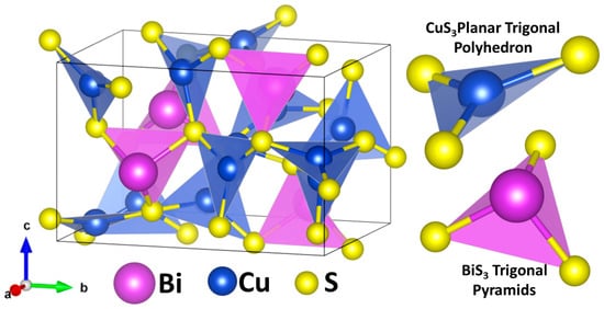
Figure 1.
Orthorhombic crystal structure of Cu3BiS3 Wittichenite-phase, with CuS3 flat coordination and BiS3 trigonal pyramids.
The orthorhombic symmetry of CBS enables direct electronic transitions [35] and contributes to a high optical absorption coefficient [36]. Chalapathi et al. produced orthorhombic CBS thin films via evaporation and sulfurization, noting improved carrier mobility and a 1.32 eV band gap energy due to reduced grain size [29].
Hussain et al. achieved p-type electrical conductivity of 0.03 Ω−1.cm−1 in CBS thin films using a combined chemical and thermal process, highlighting its potential for PV cell production [37].
Fazal et al. demonstrated that chemically deposited CBS thin films exhibit optical band gap energies ranging from 1.0 to 1.25 eV, a Hall mobility of 34.9 cm2 V−1 s−1, a charge carrier concentration of 6.07 × 1016 cm−3, and a resistivity of 7.22 Ω.cm at a thickness of 126 nm. These results suggest well-formed films with the potential for PV applications [38].
Future research can investigate how advancements in deposition methods affect the efficiency and stability of CBS thin films for photovoltaic applications [38,39,40]. Post-processing techniques like optimized heat treatments have been explored to enhance the chemical stability and conductivity of these films, rendering them more suitable for electronic devices and high-efficiency solar cells [18,34,41,42].
3. Density Functional Theory Studies
Density Functional Theory (DFT) first principles calculations serve as a powerful tool to gain deeper insights into how each constituent of the CBD Wittichenite phase influences its physical properties. By integrating experimental findings, DFT can expedite CBS research by elucidating underlying mechanisms and trends discerned from experimental data.
Whittles et al. carried out an exhaustive investigation into the alignment and width of the forbidden band, as well as the state of the valence band of CBS, employing DFT calculations considering the hybrid HSE06 functional with Spin-Orbit Coupling (SOC) in conjunction with X-ray absorption and X-ray photoemission spectroscopy (XPS) analyses [41]. Their findings reveal the presence of a type II band alignment between CBS and CdS. This suggests that using a more suitable n-type layer, which would create a type I heterostructure with a small conduction band offset, could lead to improved PCEs (Figure 2a). Furthermore, they predict a direct band gap energy of 1.18 eV at the Gamma point (Γ) and argue that it deviates from the often reported 1.4−1.5 eV due to the low density of states at the valence band maximum (VBM), as illustrated in Figure 2b. Nevertheless, this direct band gap value remains close to the optimal 1.4 eV, making it suitable for PV cell applications.
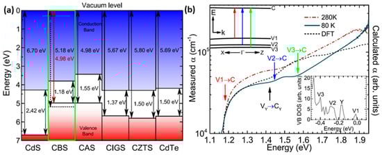
Figure 2.
(a) Band diagram aligned with the vacuum energy level for CBS and other absorber materials with the n-type layer, CdS. (b) Optical absorption spectra from CBS compared with DFT results. The upper inset is a schematic representation of the CBS band structure and absorption transitions around the Γ point. The lower inset consists of the DFT density of states at the top of the valence band. Figures reproduced with permission from [41]. Copyright 2019 American Chemical Society.
DFT studies also suggest that the VBM is primarily composed of Cu-d and Cu-sp states, with minimal influence from Bi-s states, whereas the conduction band minimum (CBM) is primarily composed of Bi-p and Bi-sp anti-ligand states [39,43,44].
Oubakalla et al. performed full-potential linearized augmented-plane-wave (FP-LAPW) DFT calculations considering the Generalized Gradient Approximation (GGA) with the Tran-Blaha modified Becke–Johnson (TB-mBJ) functional with a Hubbard potential (GGA + U + TB-mBJ) to investigate the optical and electronic properties of CBS thin films produced by co-electrodeposition in aqueous solution [43]. They predicted band gaps for CBS ranging from 1.42 to 1.52 eV, depending on the applied potential. These results aligned closely with experimental observations, suggesting the potential of this method to tune the CBS band gap.
Prudhvi Raju et al. explored the sonochemical synthesis of CBS quantum dots through a combined experimental and theoretical approach [44]. Employing FP-LAPW DFT calculations with GGA using the Perdew, Burke, and Ernzerhof (PBE) and TB-mBJ functionals, with and without SOC, they investigated the structural, electronic, and optical properties of the quantum dots. The results unveiled a transition in the band gap from direct to indirect due to the combination of Bi-p and Cu-d states in the conduction band spectra, leading to band degeneration with the inclusion of SOC, as illustrated by the electronic band structure in Figure 3a. Figure 3b shows that the VB Total Density of States (TDOS) calculated by DFT using the TB-mBJ functional is consistent with the experimental VB XPS spectrum, despite the underestimated band gap (≈1 eV) when compared to the experimental value (≈1.4 eV)
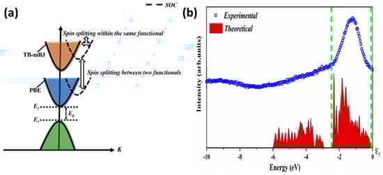
Figure 3.
(a) General illustration of spin splitting in the PBE and TB-mBJ functionals and (b) comparative VB TDOS obtained from DFT and experimental VB spectrum obtained from XPS. Figures reproduced with permission from [44]. License number 5783720881375.
These findings highlight the substantial impact of SOC on the optical and electronic characteristics of CBS quantum dots, indicating their high potential for optoelectronic device applications.
Morales-Gallardo et al. employed DFT calculations with the GGA PBE functional to assess the electronic structure properties of CBS and determine photovoltaic parameters [45]. They focused on CBS band alignments with various n-type layers (CdS, ZnO, ZnS, CdS/ZnO, CdS/ZnS, and TiO2). The study predicts that the CdS/ZnS combination exhibits excellent energy alignment with a near-zero conduction band offset, making it the most promising composite material among these heterojunctions. The authors suggest that this theoretical approach could be valuable for designing heterojunctions to enhance solar cell performance.
Jia et al. utilized DFT calculations to explore the impact of two-dimensional coordination in CBS on out-of-plane phonon scattering, which resulted in remarkably low thermal conductivity [46]. Their analysis of the phonon spectrum indicated that this property renders CBS suitable for applications demanding thermal insulation, owing to its distinctive structure that facilitates phonon scattering. This suggests potential applications of CBS beyond photovoltaics.
4. CBS Film Synthesis Methods
Several studies propose synthesis methods for CBS films. Some rely on one-step processes, where the ternary phase forms in a single process. However, in most cases, subsequent annealing is required to improve CBS’s crystallinity.
Alternatively, two-step CBS synthesis methods are also reported. These involve depositing precursor layers (such as Cu and Bi metallic layers or Cu-S and Bi-S layers), followed by an annealing or sulfurization process to form the CBS phase [47].
4.1. One-Step Processing
4.1.1. Sputtering on Heated Substrate
Sputtering deposition can be used to produce compact CBS thin films with suitable optoelectrical properties in a single step by depositing CBS precursors onto a heated substrate. Haber et al. employed RF sputtering in a 5 mTorr Ar atmosphere to cosputter CuS and Bi targets at 80 and 10 W, respectively, onto fused silica substrates heated at 250 and 300 °C [17]. To obtain a 3:1:3 (Cu:Bi:S) stoichiometry, the sputtering of the CuS target remained active while the Bi sputtering was periodically switched on and off to achieve the correct elemental ratio. They observed that the film deposited at 300 °C was homogeneous throughout its depth, while the one deposited at 250 °C retained a layered structure.
Annealing processes performed within the 250–300 °C range for 2 h under a 50 Torr (1 Torr H2S and 49 Torr Ar) atmosphere enhanced the crystallinity of the films produced by sputtering.
This single-step method, based on sputtering deposition on heated substrates, yielded CBS thin films with an average thickness of approximately 600 nm. These films exhibited an absorption coefficient ɑ ≈ 105 cm−1, sheet resistances as low as 1.6 × 10⁵ Ω, and band gaps close to the optimal 1.4 eV [17].
4.1.2. Thermal Evaporation on Heated Substrates
Hussain et al. used thermal evaporation to deposit CBS on soda–lime glass (SLG) substrates by co-evaporating anhydrous powder of copper (I) sulfide (Cu2S) and bismuth sulfide (Bi2S3). In their study, besides room temperature depositions, the films were also deposited on substrates heated at temperatures ranging from 250 to 400 °C to promote the formation of the CBS Wittichenite ternary phase [37].
The authors observed that films deposited at room temperature were amorphous and, through Energy Dispersive X-ray Spectroscopy (EDS) analysis, they demonstrated substantial composition heterogeneity across the film surface, with variations in Cu and Bi composition as high as 33 and 12 percentual points, respectively. The CBS films deposited between 250 and 350 °C were still mostly amorphous. However, films deposited on substrates at 350 and 400 °C exhibited diffraction patterns corresponding to the desired CBS Wittichenite phase. For these films, the average crystallite size of the CBS films increased from 38.4 ± 0.1 nm to 44.2 ± 0.1 nm as the substrate deposition temperature rose.
The deposition temperature also impacted the morphology of the resulting CBS films, creating more compact and columnar structures, reducing PV losses due to recombination processes [48]. Additionally, Figure 4a illustrates how the deposition temperature significantly influenced the films’ band gap energies, decreasing from 2 eV for room-temperature deposition to a value near the optimal 1.4 eV for depositions conducted at 400 °C [49,50].
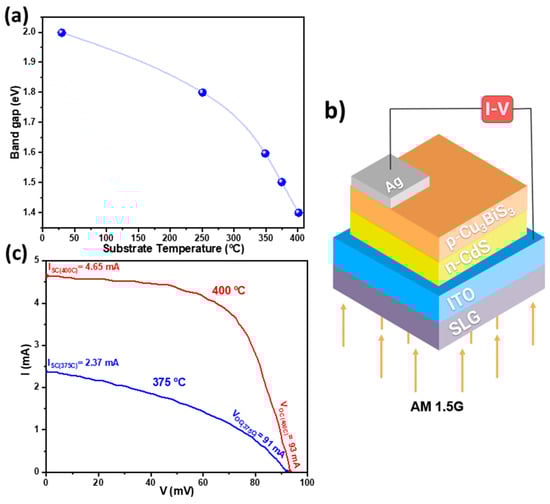
Figure 4.
(a) Band gap energies as a function of the substrate temperature. (b) SLG/ITO/n-CdS/p-CBS-Ag solar cell assembly diagram. (c) Current–voltage (I-V) plot of the solar cell. Figures were reconstructed based on data from Hussain et al. [37].
The authors also performed photocurrent–voltage measurements under AM 1.5G standard conditions of solar cells with the geometry shown in Figure 4b, using CBS films deposited at 375 and 400 °C. The I-V curves presented in Figure 4c demonstrate the enhanced PV performance of the cell utilizing the CBS film deposited at 400 °C compared to its 375 °C counterpart. The open circuit voltage (), short circuit current (), fill factor (FF), and PCE () improved from , , and to , , and . Notwithstanding, these PCEs fall significantly short of the practical thresholds.
4.1.3. Spin Coating
Spin coating offers an interesting, cost-effective, one-step method for CBS synthesis. Jiajia Li et al. adopted a low-cost, solution-based process of dimethyl sulfoxide (DMSO) without the need for post-sulfurization, using CuCl, BiCl3, thiourea, and DMSO for the precursor solutions, to successfully produce CBS films [51]. Mo-coated SLG samples were placed on a sample holder and spin-coated at 3000 rpm for 30 s. Subsequently, they were dried at temperatures ranging from 240 to 340 °C for 2 min in a N2 atmosphere.
The formation of a pure CBS phase occurred during the precursor heating stage. While the CBS films exhibited good crystallinity and a close-to-ideal band gap energy , they also displayed pores and cracks. These issues were mitigated by increasing the CBS grain size with adjustments to the drying temperatures.
The CBS films were utilized to fabricate PV cells incorporating a CdS n-type layer and a ZnO and ITO optical window, as illustrated in Figure 5a. Despite the reported high-quality CBS film, the resulting PV cells exhibited only a 0.17% PCE (), which falls substantially behind the typical PV cell efficiency standards.
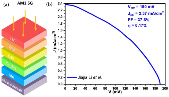
Figure 5.
(a) PV cell geometry, (b) Photocurrent–voltage curve for the spin-coated CBS PV cells. Figures were reconstructed based on data from Jiajia Li et al. [51].
4.1.4. Chemical Bath Deposition
The chemical bath deposition (CBD) technique is widely utilized for depositing sulfides, selenides, oxides, and ternary compounds [52]. It offers several advantages over other deposition methods like thermal evaporation, magnetron sputtering, and spray pyrolysis. CBD does not require high vacuum conditions or high-power sources and it can be performed at low temperatures [53], making it cheaper than the aforementioned alternative processes. Moreover, CBD allows for the deposition of films over larger areas with relative ease of control over treatment parameters [54]. Its simplicity, replicability, and scalability make it appealing for commercial production processes [52].
Deshmukh et al. were the first to produce CBS films using CBD [54] successfully. They synthesized ternary Cu3BiS3 thin films on glass slides using C4H5CuO4.H2O, Bi(NO3)3.5H2O, and CH4N2S (thiourea) precursors at 328 K for 50 min. These films exhibited high optical absorption within the visible range, with band gap energies ranging between 1.56 and 1.58 eV. X-ray diffraction (XRD) diffractograms revealed that the films were amorphous, although Scanning Electron Microscopy (SEM) micrographs displayed densely packed, fine, spherical nanoparticles measuring 70–80 nm in diameter across the sample surface, as depicted in Figure 6a,b. Still, EDS analysis indicated the presence of nearly stoichiometric CBS, with atomic percentage values for Cu, Bi, and S at 41.00%, 13.14%, and 45.82%, respectively.
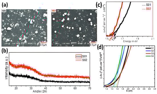
Figure 6.
(a) SEM micrographs of the surface of CBS films deposited by CBD with higher (S01) and lower (S02) concentrations, (b) diffractograms of samples S01 and S02, (c) band gap estimation of CBS thin films without (S01 and S02), and (d) band gap estimation of CBS thin films with annealing (S1, S2, S3, and S4). Figures (a–c) reproduced with permission from [54]. License number 5787110776361. Figure (d) was reconstructed based on data from Deshmukh et al. [55].
The same researchers also utilized CBD to fabricate CBS films using CuCl2.2H2O, Bi(NO3)3.5H2O, and CH4N2S (thiocarbamide) precursors [55]. By changing the concentrations of the solutions and subjecting them to subsequent annealing at 573 and 673 K, they produced CBS thin films with different morphologies, crystallinity, and band gap values ranging from 1.42 to 1.56 eV. In contrast to their initial findings, all these films exhibited crystalline phases, with those synthesized using lower reagent concentrations and higher annealing temperatures demonstrating increased crystallinity and band gap values closer to the ideal 1.34 eV, as per the Shockley–Queisser limit (Figure 6c,d).
Although CBD-produced films are promising and straightforward to produce, the absence of actual PV cells made from them hinders the assessment of their potential to yield competitive PV devices. Considering its simplicity, CBD could serve as a significant alternative to investigate the intrinsic defects observed in CBS films documented in the literature.
4.1.5. Spray Deposition
Chemical spray pyrolysis from methanol solutions using compressed air as the carrier gas offers another avenue for CBS film production, as demonstrated by Sheng Liu et al. They utilized a solution comprising CuCl2, BiCl3, and thiourea for this purpose [56]. Spray pyrolysis is known for its versatility and cost-effectiveness and can be implemented on a large scale [57,58].
Sheng Liu et al. observed that their CBS films, with an average thickness of 260 nm, displayed strong adhesion to the glass substrate. However, XRD analysis revealed the presence of secondary phases such as CuxS, Bi2S3, and CuBiS2, and the morphology of the films exhibited poor uniformity [56].
Regarding their optical properties, CBS films deposited using spray pyrolysis presented band gaps ranging from 1.65 to 1.72 eV.
4.2. Two-Step Processing
4.2.1. Thermal Evaporation of Precursors and Post-Sulfurization
Chalapathi et al. used thermal evaporation to deposit metallic precursors in a Cu/Bi/Cu configuration, followed by sulfurization inside a graphite box placed in a quartz tube furnace [29]. The graphite box contained solid sulfur to facilitate the reaction kinetics required to produce the CBS Wittichenite phase. The quartz tube furnace was heated at a rate of 10 °C/min and maintained at 350, 400, and 450 °C for 60 min.
The characterization results demonstrated crystalline CBS films with minimal secondary phases, which became increasingly suppressed with higher temperatures (Figure 7a). Additionally, SEM micrographs showed that grain size increased with the sulfurization temperature. On the other hand, elevating the temperature during the second processing step led to a decrease in resistivity and band gap energy from approximately 1.4 to 1.3 eV (Figure 7b).
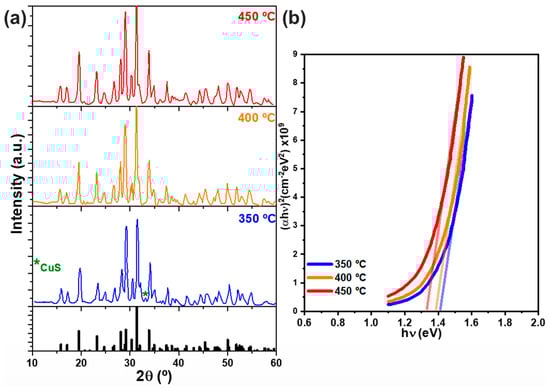
Figure 7.
(a) CBS thin film diffractograms. (b) Modified Tauc plot and estimated band gap energies for samples sulfurized at 350, 400, and 450 °C. Figures were reconstructed based on data from Chalapathi et al. [29].
The temperature of synthesis also enhanced the mobility and charge concentration, as determined by Hall effect measurements. For instance, the sample sulfurized at 450 °C presented a resistivity of 29.80 ± 0.05 Ω cm, mobility of 6.0 ± 0.2 cm2 V−1 s−1, and carrier concentration of 4.7 ± 0.5 × 1016 cm−3.
Yang et al. also employed a two-step synthesis method to prepare CBS thin films. Initially, they used co-evaporation to deposit Bi and CuS precursors in a Bi/CuS/Bi/CuS configuration [21]. The layer thicknesses were carefully controlled to achieve the ideal atomic ratio for forming a pure-phase CBS thin film [41,47,59]. Subsequently, S powders and a gas mixture of H and Ar were utilized in the annealing step, conducted at temperatures ranging from 350 to 475 °C, to facilitate the formation of CBS.
The authors reported that increasing the annealing temperature led to a rise in the number of grains assigned to the CBS film, with secondary phases present in all samples. In fact, for samples annealed at higher temperatures (400 to 450 °C), the formation of CuBiS2 was observed.
Furthermore, the Cu/Bi ratio varied depending on the layer configuration from the initial step, affecting the film composition. A Cu/Bi ratio of 3 resulted in improved crystallinity of the Cu-Bi-S films.
Despite the films’ high absorption coefficients and p-type conduction, Hall effect measurements revealed low mobility of the charge carriers, reaching a maximum of 1.5 cm2 V−1 s−1. Finally, the obtained CBS films were utilized to fabricate a PV cell with a Mo/CBS/CdS/ZnO/ZnO:Al/NiAl geometry, achieving an efficiency of 1.7%, the highest efficiency reported to date [21].
4.2.2. Sputtering Deposition of Precursors and Post-Sulfurization
Gerein et al. used DC sputtering to deposit multilayers of Cu and Bi precursors onto quartz substrates from metallic targets, ensuring a 3:1 Cu to Bi ratio by using equal sputtering times. Sulfurization of the precursors took place inside the deposition chamber with 50 Torr of H2S (99.9%) at temperatures ranging from 250 to 400 °C [60].
The authors investigated the impact of sulfurization temperature and duration, as well as subsequent annealing conditions in a H2S environment, on the quality of the resulting films.
The utilization of backscattered electrons enabled the distinct visualization of two distinct phases, particularly noticeable in films subjected to higher sulfurization temperatures. This phenomenon arose from the evaporation of Bi from the films, which altered the overall reaction kinetics of the film formation process. The research revealed that conducting reactive annealing of binary precursor films at lower temperatures for prolonged durations favored the synthesis of CBS, with the most favorable outcome observed at 270 °C for 30 h, despite the challenges posed by Bi volatility.
4.2.3. Electrodeposition and Sulfurization
Electrodeposition has been effectively utilized to deposit metal precursors, subsequently converted into chalcogenides through a thermal process, yielding good results for CZTS devices [61]. One of the main features of this method is the quality and uniformity of the deposited films.
Colombara et al. employed electrodeposition to deposit Cu/Bi/Cu layers on Mo-coated SLG [33]. Subsequently, the multilayer films obtained through electrodeposition were subjected to annealing in a graphite box with excess sulfur (0.05 g) using an AS-Micro Rapid Thermal Processor (RTP) (AnnealSys). Annealing temperatures ranged from 270 to 550 °C over periods spanning from 5 to 960 min and heating rates ranged from 5 and 600 °C min−1.
The authors observed that films sulfurized below 400 °C solely exhibited binary phases (CuS and Bi2S3). Conversely, temperatures exceeding 400 °C facilitated the required reaction kinetics to form the ternary CBS Wittichenite phase and increased crystallinity in films sulfurized at 450 and 500 °C. Compact and homogeneous CBS films were achieved by sulfurizing the precursors at 500 °C for 30 min with a heating rate of 5 °C.min−1. However, higher heating rates led to film peeling off.
A summary of all synthesis methods here presented can be found in Table 2.
Table 2.
Comparison between Cu3BiS3 thin film synthesis methods.
5. CBS PV Cell Modeling
Theoretical modeling is a powerful tool to guide the study and refinement of PV devices based on novel absorber layers. Nevertheless, research on CBS as a p-type absorber layer for PV devices is limited to only two simulation studies. The first, by Mesa et al., used the updated version AMPS (Analysis of Microelectronic and Photonic Structures), wxAMPS, and SCAPS-1D (solar cell capacitance simulator) to perform the simulations [62], while the other, by Capistran-Martinez et al., relied solely on SCAPS-1D [27].
Mesa et al. claimed and based on the simulated J-V curves shown in Figure 8a [62]. However, they did not provide details on the parameters adopted or the PV geometry, including the n-type layer and the optical window used.
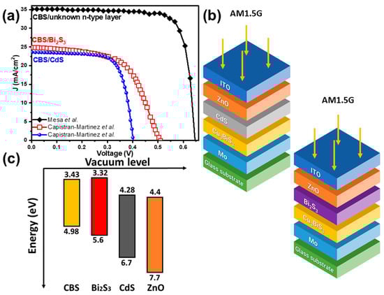
Figure 8.
(a) J-V curves simulated using wxAMP and SCAPS [27,62], (b) PV cell geometries employed in the SCAPS simulations [27], and (c) band diagrams for CBS and the n-type and ZnO layers. Figures were reconstructed based on data from Capistran-Martinez et al. [27,62].
On the other hand, Capistran-Martinez et al. conducted a comprehensive study comparing two different heterojunctions (CBS/CdS and CBS/Bi2S3) to assess the impact of n-type layers on the PV device. While CdS is commonly used as an n-type layer in p-n heterojunctions, issues with the CBS/CdS interface have been widely reported. [27,41]. To address this, the authors opted for Bi2S3 as the n-type layer in their SCAPS simulation. Bi2S3 was chosen because Cu+ ion diffusion enhances its n-type conductivity. Moreover, both CBS and Bi2S3 share the orthorhombic phase, which facilitates lattice matching at the p-n interface [27].
They used SCAPS to model glass/Mo/CBS/CdS/ZnO/ITO and glass/Mo/CBS/Bi2S3/ZnO/ITO PV cells (Figure 8b), incorporating CBS parameters derived from experimental analyses including XRD, UV–Vis spectroscopy, and Hall effect mobility measurements. The corresponding J-V curves are presented in Figure 8a and reveal FF values of 0.72 and 0.58 and PCEs of and for cells employing CdS and Bi2S3, respectively. The energy band diagram depicted in Figure 8c illustrates superior band alignment between CBS and Bi2S3, potentially elucidating the higher efficiency observed in the CBS/Bi2S3 heterojunction compared to CBS/CdS.
It is noteworthy that despite the promising outcomes from PV cell simulations featuring a CBS absorber layer, the highest experimental reported efficiency stands at only , significantly lower than the simulated results by about one order of magnitude [51]. This indicates the existence of significant technical challenges in experimental implementation that must be addressed before attaining the simulated efficiencies.
6. Conclusions
This review highlights the promising potential of CBS as an alternative sustainable, cost-effective absorber layer in thin film PV cells. While numerous studies have explored its optoelectronic properties, there are still many unanswered questions regarding its optimal synthesis process, structural characteristics, and device performance.
Despite being relatively unexplored compared to other generations of PV materials, CBS is gaining significant attention from the scientific community due to its sustainability, environmental friendliness, and potential cost-effectiveness.
However, for CBS to fulfill its promise as the next big PV material, higher-quality and more focused studies are required. Addressing fundamental questions surrounding film synthesis, stoichiometry control, interface engineering, and device optimization will be crucial steps towards unlocking the full potential of CBS-based PV devices. Nonetheless, the fertile research landscape surrounding CBS suggests that it may indeed emerge as a leading PV material in the near future, offering significant advantages in terms of sustainability and affordability.
Author Contributions
Conceptualization, C.d.O.A., M.S.L. and J.C.A.d.Q.; methodology, C.d.O.A., M.S.L. and J.C.A.d.Q.; formal analysis, C.d.O.A., M.S.L. and J.C.A.d.Q.; investigation, C.d.O.A., M.S.L. and J.C.A.d.Q.; writing—original draft preparation, C.d.O.A., M.S.L. and J.C.A.d.Q.; writing—review and editing, C.d.O.A., M.S.L., J.C.A.d.Q., S.M.S., T.H.d.C.C. and A.F.d.C.; visualization, C.d.O.A., M.S.L. and J.C.A.d.Q.; supervision, C.d.O.A., T.H.d.C.C. and A.F.d.C.; project administration, T.H.d.C.C. and A.F.d.C.; funding acquisition, T.H.d.C.C. and A.F.d.C. All authors have read and agreed to the published version of the manuscript.
Funding
This research was funded by FEDER funds through the COMPETE 2020 Program and National Funds through the FCT—Portuguese Foundation for Science and Technology, under the projects LISBOA-01-0247-FEDER-039985/POCI-01-0247-FEDER-039985, LA/P/0037/2020, UIDP/50025/2020, and UIDB/50025/2020 of the Associate Laboratory Institute of Nanostructures, Nanomodelling and Nanofabrication—i3N. This study was also supported by the Conselho Nacional de Desenvolvimento Científico e Tecnológico—Brasil (CNPq)—CNPq Call No. 26/2021 Support for Scientific, Technological and Innovation Research: Scholarships Abroad.
Data Availability Statement
No new data were created or analyzed in this study. Data sharing is not applicable to this article.
Conflicts of Interest
The authors declare no conflict of interests.
References
- Liu, Y.; Li, Y.; Wu, Y.; Yang, G.; Mazzarella, L.; Procel-Moya, P.; Tamboli, A.C.; Weber, K.; Boccard, M.; Isabella, O.; et al. High-Efficiency Silicon Heterojunction Solar Cells: Materials, Devices and Applications. Mater. Sci. Eng. R Rep. 2020, 142, 100579. [Google Scholar] [CrossRef]
- Lewis, N.S.; Nocera, D.G. Powering the planet: Chemical challenges in solar energy utilization. Proc. Natl. Acad. Sci. USA 2006, 103, 15729–15735. [Google Scholar] [CrossRef] [PubMed]
- Shi, B.; Duan, L.; Zhao, Y.; Luo, J.; Zhang, X. Semitransparent Perovskite Solar Cells: From Materials and Devices to Applications. Adv. Mater. 2020, 32, e1806474. [Google Scholar] [CrossRef] [PubMed]
- Alam, M.W.; Ansari, M.Z.; Aamir, M.; Waheed-Ur-Rehman, M.; Parveen, N.; Ansari, S.A. Preparation and Characterization of Cu and Al Doped ZnO Thin Films for Solar Cell Applications. Crystals 2022, 12, 128. [Google Scholar] [CrossRef]
- Mesa, F.; Dussan, A.; Gordillo, G. Study of the growth process and optoelectrical properties of nanocrystalline Cu3BiS3 thin films. Phys. Status Solidi C 2010, 7, 917–920. [Google Scholar] [CrossRef]
- Ramanujam, J.; Bishop, D.M.; Todorov, T.K.; Gunawan, O.; Rath, J.; Nekovei, R.; Artegiani, E.; Romeo, A. Flexible CIGS, CdTe and a-Si:H based thin film solar cells: A review. Prog. Mater. Sci. 2020, 110, 100619. [Google Scholar] [CrossRef]
- Kumar, M.; Dubey, A.; Adhikari, N.; Venkatesan, S.; Qiao, Q. Strategic review of secondary phases, defects and defect-complexes in kesterite CZTS–Se solar cells. Energy Environ. Sci. 2015, 8, 3134–3159. [Google Scholar] [CrossRef]
- Lee, T.D.; Ebong, A.U. A review of thin film solar cell technologies and challenges. Renew. Sustain. Energy Rev. 2017, 70, 1286–1297. [Google Scholar] [CrossRef]
- Powalla, M.; Paetel, S.; Ahlswede, E.; Wuerz, R.; Wessendorf, C.D.; Friedlmeier, T.M. Thin-film solar cells exceeding 22% solar cell efficiency: An overview on CdTe-, Cu(In,Ga)Se2-, and perovskite-based materials. Appl. Phys. Rev. 2018, 5, 041602. [Google Scholar] [CrossRef]
- Shah, U.A.; Wang, A.; Ullah, M.I.; Ishaq, M.; Alam Shah, I.; Zeng, Y.; Abbasi, M.S.; Umair, M.A.; Farooq, U.; Liang, G.; et al. A Deep Dive into Cu2ZnSnS4 (CZTS) Solar Cells: A Review of Exploring Roadblocks, Breakthroughs, and Shaping the Future. Small 2024, e2310584. [Google Scholar] [CrossRef]
- Green, M.; Dunlop, E.; Hohl-Ebinger, J.; Yoshita, M.; Kopidakis, N.; Hao, X. Solar cell efficiency tables (version 57. Prog. Photovolt. Res. Appl. 2021, 29, 3–15. [Google Scholar] [CrossRef]
- Best Research-Cell Efficiency Chart. Acedido: 13 de maio de 2024. [Em linha]. Available online: https://www.nrel.gov/pv/cell-efficiency.html (accessed on 15 May 2020).
- Konstantakou, M.; Perganti, D.; Falaras, P.; Stergiopoulos, T. Anti-Solvent Crystallization Strategies for Highly Efficient Perovskite Solar Cells. Crystals 2017, 7, 291. [Google Scholar] [CrossRef]
- Zyoud, S.H.; Zyoud, A.H.; Ahmed, N.M.; Prasad, A.R.; Khan, S.N.; Abdelkader, A.F.I.; Shahwan, M. Numerical Modeling of High Conversion Efficiency FTO/ZnO/CdS/CZTS/MO Thin Film-Based Solar Cells: Using SCAPS-1D Software. Crystals 2021, 11, 1468. [Google Scholar] [CrossRef]
- Wang, W.; Winkler, M.T.; Gunawan, O.; Gokmen, T.; Todorov, T.K.; Zhu, Y.; Mitzi, D.B. Device Characteristics of CZTSSe Thin-Film Solar Cells with 12.6% Efficiency. Adv. Energy Mater. 2014, 4, 1301465. [Google Scholar] [CrossRef]
- Mineral Commodity Summaries 2023; U.S. Geological Survey, Summaries; 2023. Available online: https://pubs.usgs.gov/periodicals/mcs2023/mcs2023.pdf (accessed on 26 May 2024).
- Gerein, N.J.; Haber, J.A. One-Step Synthesis and Optical and Electrical Properties of Thin Film Cu3BiS3 for Use as a Solar Absorber in Photovoltaic Devices. Chem. Mater. 2006, 18, 6297–6302. [Google Scholar] [CrossRef]
- Deshmukh, S.G.; Kheraj, V. A comprehensive review on synthesis and characterizations of Cu3BiS3 thin films for solar photovoltaics. Nanotechnol. Environ. Eng. 2017, 2, 15. [Google Scholar] [CrossRef]
- Ojebuoboh, F.K. Bismuth—Production, properties, and applications. JOM 1992, 44, 46–49. [Google Scholar] [CrossRef]
- Wang, S.; Lu, P. (Eds.) Bismuth-Containing Alloys and Nanostructures; Springer Series in Materials Science; Springer: Singapore, 2019; Volume 285. [Google Scholar] [CrossRef]
- Yang, Y.; Xiong, X.; Yin, H.; Zhao, M.; Han, J. Study of copper bismuth sulfide thin films for the photovoltaic application. J. Mater. Sci. Mater. Electron. 2019, 30, 1832–1837. [Google Scholar] [CrossRef]
- Daniel, T.; Balasubramanian, V.; Nishanthi, S.T.; Amudhavalli, K.; Sivakumar, G.; Mohanraj, K. Photoelectrochemical and photovoltaic cell performances of thermally evaporated Cu3BiS3 thin films. Vacuum 2022, 195, 110707. [Google Scholar] [CrossRef]
- Kehoe, A.B.; Temple, D.J.; Watson, G.W.; Scanlon, D.O. Cu3MCh3 (M = Sb, Bi; Ch = S, Se) as candidate solar cell absorbers: Insights from theory. Phys. Chem. Chem. Phys. 2013, 15, 15477–15484. [Google Scholar] [CrossRef]
- Yin, J.; Jia, J. Synthesis of Cu 3 BiS 3 nanosheet films on TiO2 nanorod arrays by a solvothermal route and their photoelectrochemical characteristics. CrystEngComm 2014, 16, 2795–2801. [Google Scholar] [CrossRef]
- Hernadez-Mota, J.; Espindola-Rodriguez, M.; Sanchez, Y.; Lopez, I.; Pena, Y.; Saucedo, E. Thin film photovoltaic devices prepared with Cu3BiS3 ternary compound. Mater. Sci. Semicond. Process. 2018, 87, 37–43. [Google Scholar] [CrossRef]
- Fang, Y.; Zhao, W.; Li, W.; Han, X. Effects of thiourea dosage on the structural, optical and electrical properties of one-step solution processed Cu3BiS3 film for photovoltaics. Appl. Phys. A 2021, 127, 1–6. [Google Scholar] [CrossRef]
- Capistrán-Martínez, J.; Loeza-Díaz, D.; Mora-Herrera, D.; Pérez-Rodríguez, F.; Pal, M. Theoretical evaluation of emerging Cd-free Cu3BiS3 based solar cells using experimental data of chemically deposited Cu3BiS3 thin films. J. Alloys Compd. 2021, 867, 159156. [Google Scholar] [CrossRef]
- Santos, D.R.; Shukla, S.; Vermang, B. Prospects of copper–bismuth chalcogenide absorbers for photovoltaics and photoelectrocatalysis. J. Mater. Chem. A 2023, 11, 22087–22104. [Google Scholar] [CrossRef]
- Chalapathi, U.; Mallikarjuna, K.; Kumar, K.C.; Gonuguntla, V.; El-Marghany, A.; Rosaiah, P.; Park, S.-H. Fabrication of phase-pure and large-grained Cu3BiS3 films by a two-stage process for thin film solar cells. Solid State Sci. 2024, 151, 107522. [Google Scholar] [CrossRef]
- Rath, T.; Marin-Beloqui, J.M.; Bai, X.; Knall, A.-C.; Sigl, M.; Warchomicka, F.G.; Griesser, T.; Amenitsch, H.; Haque, S.A. Solution-Processable Cu3BiS3 Thin Films: Growth Process Insights and Increased Charge Generation Properties by Interface Modification. ACS Appl. Mater. Interfaces 2023, 15, 41624–41633. [Google Scholar] [CrossRef] [PubMed]
- Kocman, V.; Nuffield, E.W. The crystal structure of wittichenite, Cu3BiS3. Acta Crystallogr. B 1973, 29, 2528–2535. [Google Scholar] [CrossRef]
- Evans, H.T. The crystal structures of low chalcocite and djurleite. Z. Für Krist. Cryst. Mater. 1979, 150, 299–320. [Google Scholar] [CrossRef]
- Colombara, D.; Peter, L.; Hutchings, K.; Rogers, K.; Schäfer, S.; Dufton, J.; Islam, M. Formation of Cu3BiS3 thin films via sulfurization of Bi–Cu metal precursors. Thin Solid Films 2012, 520, 5165–5171. [Google Scholar] [CrossRef]
- Lundegaard, L.F.; Makovicky, E.; Boffa-Ballaran, T.; Balic-Zunic, T. Crystal structure and cation lone electron pair activity of Bi2S3 between 0 and 10 GPa. Phys. Chem. Miner. 2005, 32, 578–584. [Google Scholar] [CrossRef]
- Moon, S.; Park, J.; Lee, H.; Yang, J.W.; Yun, J.; Park, Y.S.; Lee, J.; Im, H.; Jang, H.W.; Yang, W.; et al. Bi2S3-Cu3BiS3 Mixed Phase Interlayer for High-Performance Cu3BiS3-Photocathode for 2.33% Unassisted Solar Water Splitting Efficiency. Adv. Sci. 2023, 10, e2206286. [Google Scholar] [CrossRef] [PubMed]
- Zhao, W.; Fang, Y.; Li, W.; Han, X. Impact of Ag doping on Cu3BiS3 solar cell performance. Sol. Energy 2021, 221, 109–113. [Google Scholar] [CrossRef]
- Hussain, A.; Luo, J.T.; Fan, P.; Liang, G.; Su, Z.; Ahmed, R.; Ali, N.; Wei, Q.; Muhammad, S.; Chaudhry, A.R.; et al. p-type Cu3BiS3 thin films for solar cell absorber layer via one stage thermal evaporation. Appl. Surf. Sci. 2020, 505, 144597. [Google Scholar] [CrossRef]
- Fazal, T.; Iqbal, S.; Shah, M.; Mahmood, Q.; Ismail, B.; Alsaab, H.O.; Awwad, N.S.; Ibrahium, H.A.; Elkaeed, E.B. Optoelectronic, structural and morphological analysis of Cu3BiS3 sulfosalt thin films. Results Phys. 2022, 36, 105453. [Google Scholar] [CrossRef]
- Mahto, B.; Khan, A.A.; Barhoi, A.; Hussain, S. Hierarchical Cu3BiS3 Nanostructures with Thermally Controlled Morphology for Photoconductive, Photothermal, and Catalytic Applications. ACS Appl. Nano Mater. 2023, 6, 6784–6797. [Google Scholar] [CrossRef]
- Deshmukh, S.G.; Kheraj, V.; Karande, K.J.; Panchal, A.K.; Deshmukh, R.S. Deshmukh, Hierarchical flower-like Cu3BiS3 thin film synthesis with non-vacuum chemical bath deposition technique. Mater. Res. Express 2019, 6, 084013. [Google Scholar] [CrossRef]
- Whittles, T.J.; Veal, T.D.; Savory, C.N.; Yates, P.J.; Murgatroyd, P.A.E.; Gibbon, J.T.; Birkett, M.; Potter, R.J.; Major, J.D.; Durose, K.; et al. Band Alignments, Band Gap, Core Levels, and Valence Band States in Cu3BiS3 for Photovoltaics. ACS Appl. Mater. Interfaces 2019, 11, 27033–27047. [Google Scholar] [CrossRef] [PubMed]
- Wu, X.; Zhao, W.; Hu, Y.; Xiao, G.; Ni, H.; Ikeda, S.; Ng, Y.; Jiang, F. Research on the Influence of the Interfacial Properties Between a Cu3BiS3 Film and an InxCd1−xS Buffer Layer for Photoelectrochemical Water Splitting. Adv. Sci. 2022, 9, e2204029. [Google Scholar] [CrossRef]
- Oubakalla, M.; Bouachri, M.; Beraich, M.; Taibi, M.; Guenbour, A.; Bellaouchou, A.; Bentiss, F.; Zarrouk, A.; Fahoume, M. Potential Effect on the Properties of Cu3BiS3 Thin Film Co-electrodeposited in Aqueous Solution Enriched Using DFT Calculation. J. Electron. Mater. 2022, 51, 7223–7233. [Google Scholar] [CrossRef]
- Raju, N.P.; Tripathi, D.; Lahiri, S.; Thangavel, R. Heat reflux sonochemical synthesis of Cu3BiS3 quantum dots: Experimental and first-principles investigation of spin–orbit coupling on structural, electronic, and optical properties. Sol. Energy 2023, 259, 107–118. [Google Scholar] [CrossRef]
- Morales-Gallardo, M.; Pascoe-Sussoni, J.E.; Delesma, C.; Mathew, X.; Paraguay-Delgado, F.; Muñiz, J.; Mathews, N. Surfactant free solvothermal synthesis of Cu3BiS3 nanoparticles and the study of band alignments with n-type window layers for applications in solar cells: Experimental and theoretical approach. J. Alloys Compd. 2021, 866, 158447. [Google Scholar] [CrossRef]
- Jia, F.; Zhao, S.; Wu, J.; Chen, L.; Liu, T.; Wu, L. Cu3BiS3: Two-Dimensional Coordination Induces Out-of-Plane Phonon Scattering Enabling Ultralow Thermal Conductivity. Angew. Chem. 2023, 135, e202315642. [Google Scholar] [CrossRef]
- Chalapathi, U.; Prasad, P.R.; Sambasivam, S.; Mallikharjuna, K.; Rosaiah, P.; Alhammadi, S.; Tighezza, A.M.; Mohanarangam, K.; Park, S.-H. Two-stage growth of Cu3BiS3 thin films: Influence of the Cu/Bi ratio. J. Mater. Res. Technol. 2023, 26, 2443–2450. [Google Scholar] [CrossRef]
- Li, J.; Jiang, L.; Wang, B.; Liu, F.; Yang, J.; Tang, D.; Lai, Y.; Li, J. Electrodeposition and characterization of copper bismuth selenide semiconductor thin films. Electrochim. Acta 2013, 87, 153–157. [Google Scholar] [CrossRef]
- Ali, N.; Hussain, A.; Ahmed, R.; Wang, M.K.; Zhao, C.; Haq, B.U.; Fu, Y.Q. Advances in nanostructured thin film materials for solar cell applications. Renew. Sustain. Energy Rev. 2016, 59, 726–737. [Google Scholar] [CrossRef]
- Viezbicke, B.D.; Birnie, D.P. Solvothermal Synthesis of Cu3BiS3 Enabled by Precursor Complexing. ACS Sustain. Chem. Eng. 2013, 1, 306–308. [Google Scholar] [CrossRef]
- Li, J.; Han, X.; Zhao, Y.; Li, J.; Wang, M.; Dong, C. One–step synthesis of Cu3BiS3 thin films by a dimethyl sulfoxide (DMSO)–based solution coating process for solar cell application. Sol. Energy Mater. Sol. Cells 2018, 174, 593–598. [Google Scholar] [CrossRef]
- Ezekoye, B.A.; Offor, P.O.; Ezekoye, V.A.; Ezema, F.I. Chemical Bath Deposition Technique of Thin Films: A Review. Int. J. Sci. Res. 2012, 2, 452–456. [Google Scholar] [CrossRef]
- Arsad, A.Z.; Zuhdi, A.W.M.; Abdullah, S.F.; Chau, C.F.; Ghazali, A.; Ahmad, I.; Abdullah, W.S.W. Effect of Chemical Bath Deposition Variables on the Properties of Zinc Sulfide Thin Films: A Review. Molecules 2023, 28, 2780. [Google Scholar] [CrossRef]
- Vipul, K. Chemical bath deposition of Cu3BiS3 thin films. AIP Conf. Proc. 2016, 1728, 020023. [Google Scholar] [CrossRef]
- Deshmukh, S.G.; Panchal, A.K.; Kheraj, V. Development of Cu3BiS3 thin films by chemical bath deposition route. J. Mater. Sci. Mater. Electron. 2017, 28, 11926–11933. [Google Scholar] [CrossRef]
- Liu, S.; Wang, X.; Nie, L.; Chen, L.; Yuan, R. Spray pyrolysis deposition of Cu3BiS3 thin films. Thin Solid Films 2015, 585, 72–75. [Google Scholar] [CrossRef]
- Nanu, M.; Schoonman, J.; Goossens, A. Nanocomposite Three-Dimensional Solar Cells Obtained by Chemical Spray Deposition. Nano Lett. 2005, 5, 1716–1719. [Google Scholar] [CrossRef] [PubMed]
- Faber, H.; Butz, B.; Dieker, C.; Spiecker, E.; Halik, M. Fully Patterned Low-Voltage Transparent Metal Oxide Transistors Deposited Solely by Chemical Spray Pyrolysis. Adv. Funct. Mater. 2013, 23, 2828–2834. [Google Scholar] [CrossRef]
- Chalapathi, U.; Prasad, P.R.; Reddy, C.P.; Sambasivam, S.; Rosaiah, P.; Ouladsmane, M.; Alhammadi, S.; Lee, S.; Park, S. Synthesis of wittichenite Cu3BiS3 thin films by sulfurizing thermally evaporated Cu-Bi metallic stacks. Chalcogenide Lett. 2023, 1584–8663, 797–802. [Google Scholar] [CrossRef]
- Gerein, N.J.; Haber, J.A. Physical Vapor Deposition Synthesis of Cu3BiS3 for Application in Thin Film Photovoltaics. MRS Proc. 2005, 865, 52. [Google Scholar] [CrossRef]
- Ennaoui, A.; Lux-Steiner, M.; Weber, A.; Abou-Ras, D.; Kötschau, I.; Schock, H.-W.; Schurr, R.; Hölzing, A.; Jost, S.; Hock, R.; et al. Cu2ZnSnS4 thin film solar cells from electroplated precursors: Novel low-cost perspective. Thin Solid Films 2009, 517, 2511–2514. [Google Scholar] [CrossRef]
- Mesa, F.; Ballesteros, V.; Dussan, A. Growth Analysis and Numerical Simulation of Cu_3BiS_3 Absorbing Layer Solar Cell through the wxAMPS and Finite Element Method. Acta Phys. Pol. A 2014, 125, 385–387. [Google Scholar] [CrossRef]
Disclaimer/Publisher’s Note: The statements, opinions and data contained in all publications are solely those of the individual author(s) and contributor(s) and not of MDPI and/or the editor(s). MDPI and/or the editor(s) disclaim responsibility for any injury to people or property resulting from any ideas, methods, instructions or products referred to in the content. |
© 2024 by the authors. Licensee MDPI, Basel, Switzerland. This article is an open access article distributed under the terms and conditions of the Creative Commons Attribution (CC BY) license (https://creativecommons.org/licenses/by/4.0/).