Abstract
In this work, a GaN-on-Si quasi-vertical Schottky diode was demonstrated on a locally grown n-GaN drift layer using Selective Area Growth (SAG). The diode achieved a current density of 2.5 kA/cm2, a specific on-resistance of 1.9 mΩ cm2 despite the current crowding effect in quasi-vertical structures, and an on/off current ratio (Ion/Ioff) of 1010. Temperature-dependent current–voltage characteristics were measured in the range of 313–433 K to investigate the mechanisms of leakage conduction in the device. At near-zero bias, thermionic emission (TE) was found to dominate. By increasing up to 10 V, electrons gained enough energy to excite into trap states, leading to the dominance of Frenkel–Poole emission (FPE). For a higher voltage range (−10 V to −40 V), the increased electric field facilitated the hopping of electrons along the continuum threading dislocations in the “bulk” GaN layers, and thus, variable range hopping became the main mechanism for the whole temperature range. This work provides an in-depth insight into the leakage conduction transport on pseudo-vertical GaN-on-Si Schottky barrier diodes (SBDs) grown by localized epitaxy.
1. Introduction
Wide-bandgap (WBG) materials are gaining popularity due to the increasing need for high-power, efficient and reliable semiconductor devices in sectors like the automotive industry, telecommunications and renewable energy. With silicon (Si) reaching its technological limits, materials like silicon carbide (SiC) and gallium nitride (GaN) are steadily replacing silicon-based technologies.
Gallium nitride (GaN) has become increasingly popular in the world of power devices due to its remarkable properties, such as having a wide bandgap, high electron mobility and robust breakdown field strength. These factors collectively enable GaN-based devices to offer low on-resistance (Ron) and the ability to operate efficiently at high frequencies in high-voltage applications [1,2].
Today, commercial GaN high-electron-mobility transistors (HEMTs) are constructed using lateral AlGaN/GaN heterostructures grown on substrates like Si, SiC, or sapphire. These lateral devices benefit from the two-dimensional electron gas (2DEG) that forms at the interface of the AlGaN and GaN heterostructures. However, commercial HEMT devices are limited in terms of voltage capability and cannot exceed 1 kV [3] since the current is more determined by the distance between the source and drain contacts. Significant enlargement of the lateral dimensions of the device is necessary to attain a high breakdown voltage (BV), which directly influences the on-resistance (Ron). HEMT devices commonly operate in a normally on state, necessitating specialized structures like a recess gate, ion implantation, or p-GaN to interrupt the two-dimensional electron gas (2DEG) and facilitate normally off operation [3]. However, normally off HEMT devices still encounter challenges, including instability in high threshold voltage caused by charge trapping and current collapse. An alternative structure that addresses these issues involves using vertical GaN devices grown on native GaN substrates [4,5,6,7]. Vertical GaN devices offer several advantages over lateral GaN devices, such as increased scalability, improved heat dissipation, reduced surface sensitivity, enhanced reliability and high-voltage capability (BV > 600 V).
However, the use of freestanding GaN substrates has potential for the epitaxy of strain-free GaN and the development of fully vertical device geometries [8]. However, challenges such as high production costs, variable quality, small wafer size and limited availability hinder their widespread adoption. Consequently, there has recently been a heightened focus on fabricating vertical power devices on foreign substrates such as sapphire, QSTTM and silicon [9,10]. From a commercial standpoint, silicon substrates are heavily favored. However, they present a significant challenge during GaN growth due to the mismatch in the coefficient of thermal expansion between GaN and silicon. Although this can be managed by strain engineering, total layer thickness is limited to ~14 µm, with lower drift layer thickness [11,12,13,14]. To overcome this limitation and enhance the maximum achievable breakdown voltage (BV), Selective Area Growth (SAG) or localized epitaxy emerges as a promising growth solution. Research has demonstrated that during the SAG of GaN micro pillars [13], stress is effectively reduced by elastic relaxation, allowing for an increase in the maximum epitaxial layer thickness. Other advantages of using selective epitaxy approaches include reduced growth time due to higher growth rates and simplified fabrication for quasi-vertical diodes [13].
In this work, quasi-vertical GaN Schottky barrier diodes (SBDs) grown on Si substrates using localized epitaxy were demonstrated [15], and their electrical performance in forward and reverse modes were investigated. The leakage current transport in GaN quasi-vertical SBDs on Si is likely to be different from freestanding GaN-on-GaN SBDs. The high dislocation density, resulting from the lattice constant mismatch between GaN and Si, can induce various conduction modes. Hence, comprehending the leakage current transport mechanism of GaN quasi-vertical Schottky barrier diodes (SBDs) on Si is imperative. Many researchers have indicated that variable range hopping (VRH) facilitated by dislocations serves as the principal off-state leakage mechanism in vertical GaN diodes [16]. Others have reported that the primary leakage process in GaN-on-Si SBDs varies for different reverse biases and is contingent upon the presence of edge terminations (ETs) [17,18]. The goal of this study was to understand the carrier transport processes in pseudo-vertical GaN Schottky barrier diodes (SBDs) on Si obtained by Selective Area Growth (SAG). In this work, we conducted a comprehensive investigation into the current transport mechanism of quasi-vertical GaN SBDs on Si under various bias conditions using current–voltage I–V measurements with a temperature range from 313 to 433 K.
2. Materials and Methods
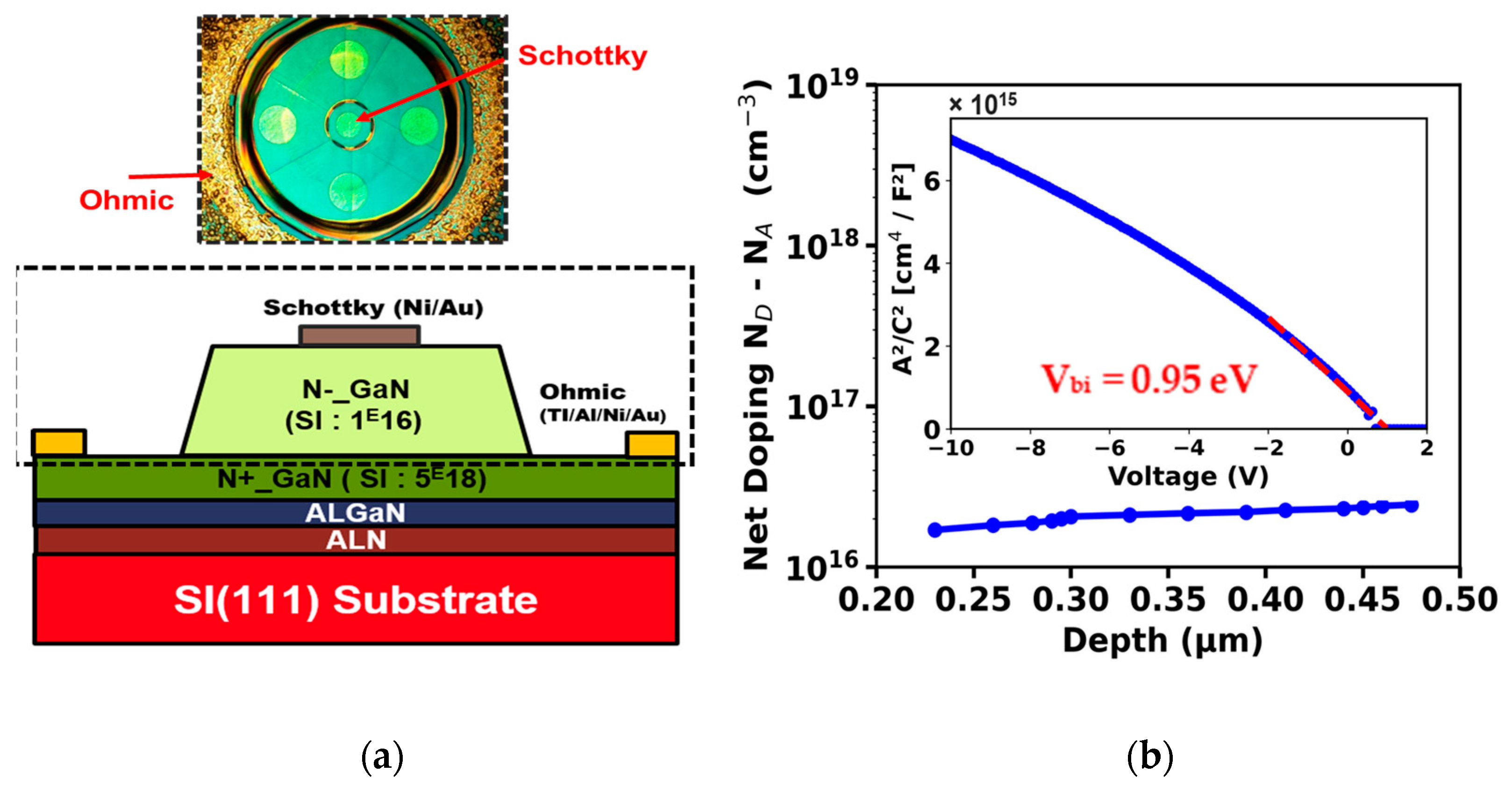
In this study, as presented in Figure 1a, samples were grown on a single-wafer fully automated AIXTRON Crius-R200 metal-organic vapour phase epitaxy (MOVPE) tool, on 200 mm diameter Si(111) wafers. The structure, from the bottom to the top, consists of AlN and AlGaN buffer layers, an undoped 300 nm thick GaN layer and three 350 nm thick n+-GaN layers acting as current spreading layers (5 × 10¹⁶, 5 × 10¹⁷ and 5 × 1018 cm−3 Si doping densities, respectively, increasing from bottom to top). The spreading layer is separated into different doping levels so that they can be used as calibration layers in other studies to examine the doping level in the drift layer on cross-section analysis [15]. A 50 nm thick Al2O3 mask was deposited on these layers by atomic layer deposition at 300 °C, and was then patterned with photolithography and etching.
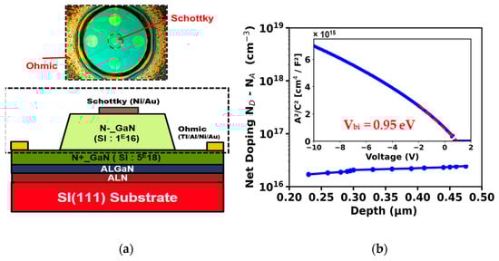
Figure 1.
(a) Schematic cross-section of quasi-vertical Schottky diode using localized epitaxy. Inset: optical microscopy of the circular measured devices. (b) Net doping concentration (ND − NA) in the n-GaN drift layer from the C-V curve at 1MHz. Inset: (A2/C2) versus the reverse voltage (The red dotted line corresponds to the fit).
Localized epitaxial growth of the drift layer was subsequently performed in the openings of this mask, demonstrating a doping concentration of ND–NA ~ 1.5 × 1016 cm−3 as showed in Figure 1b (evaluated by capacitance–voltage C-V measurements according to Equation (1). A built-in voltage Vbi = 0.95 V was also obtained from the linear extrapolation of (A2/C2) versus the voltage).
To go into more detail, an intentionally doped GaN layer was grown at 1040 °C, with a nominal growth rate of 1.5 µm/h (for full wafer growth). The pressure of the chamber was 400 mbar, the NH3 flow was set at 10 slm and the growth time was 2 h. The dopant of the layer was Si and its intended doping concentration was 1 × 1016 cm−3. The precursors for gallium and silicon were tri-methyl gallium (TMGa) and silane (SiH4), respectively. The SiH4 flow value was set as that for a full wafer growth. The Al2O3 mask was not removed after the growth.
After that, the Al2O3 mask around the mesa was etched by Cl2 and a Ti/Al/Ni/Au (95 nm/200 nm/20 nm/165 nm) metal stack was deposited on the n+ GaN as the cathode contact, followed by rapid thermal annealing (RTA) at 750 °C, to form the ohmic contacts. Finally, circular Ni/Au (50 nm/150 nm) Schottky contacts were formed on the n−GaN drift layer by a liftoff process followed by 5 min of thermal annealing at 400 °C.
3. Results
3.1. Forward Bias
Electrical characterization of the devices was performed using a 4156C Precision semiconductor parameter analyzer and a Keithley K2657 Tesla GPIB 24 parameter analyzer. The measured diodes had a diameter of 90 µm and an anode diameter of 50 µm. The current in this study was normalized using an area of cm2.
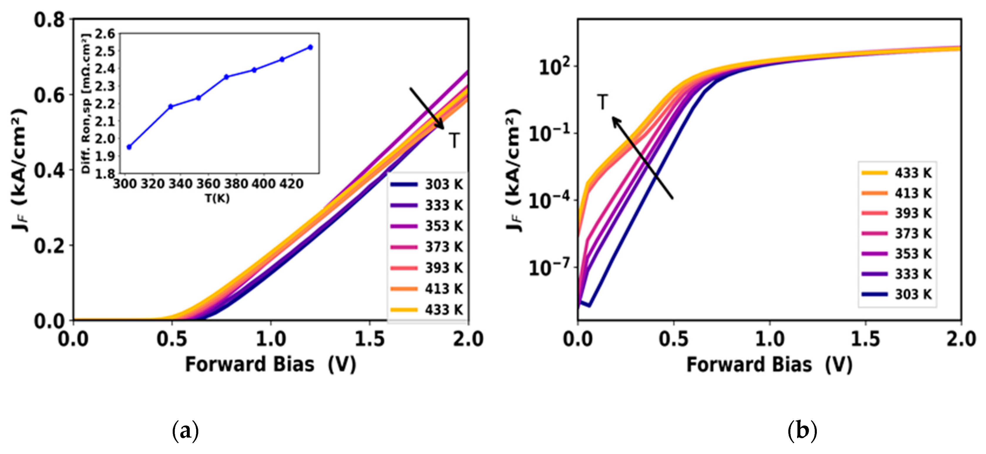
Figure 2a shows the typical forward J-V characteristics in semi-log scale obtained on a GaN pseudo-vertical Schottky diode, showing a low turn-on voltage of ~0.6 V defined at J = 1 A/cm−2 and a good on/off current ratio of . The device achieved an output current density of ~2.5 kA/cm2 and a low differential specific on-resistance of 1.9 mΩ cm2 at 5V, as shown in Figure 2b, despite the expected current crowding effect at the edges in quasi-vertical structures [19]. The ideality factor n of 1.03 and the Schottky barrier height of 0.95 eV (consistent with the extracted Schottky barrier height from C-V measurement ~1.02 eV) were extracted from Equation (2), at room temperature (RT = 300 K). The high on/off current ratio and near-unity ideality factor indicate the good quality of the Ni/n-GaN interface. These characteristics suggest efficient electron flow when the device is on and minimal leakage when the device is off, showcasing the interface’s effectiveness in controlling current. Additionally, the near-unity ideality factor implies that the diode closely follows ideal diode behavior, indicating the domination of thermionic emission (TE) [20].
where is the saturation current, A is the area of the anode contact, A* is the effective Richardson’s constant (theoretically 26.4 A/cm2 K2 for GaN), is the Schottky barrier height, q is the elementary charge (1.6 ), k is the Boltzmann’s constant, T is the temperature and n is the ideality factor.
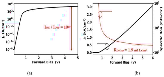
Figure 2.
Typical forward J-V curves obtained for GaN pseudo-vertical SBD in (a) semi-log and (b) linear scale, respectively.
Figure 3a,b show the typical temperature-dependent forward characteristics of the SBD. For all measured samples, the T-J-V characteristics show two trends. When V is low, the current is dominated by hot electron emission from GaN to Ni/contact across the Schottky barrier. The higher the temperature, the more electrons gain enough energy to cross the Schottky barrier, and the higher the current is. On the other hand, when V is higher, the current is limited by electron transport in the n-GaN drift region following the ohmic conduction law. As the temperature increases, the mobility of electrons decreases and the differential Ron,sp increases from 1.9 mΩ cm2 at 25 °C to 2.5 mΩ cm2 at 160 °C, probably due to the reduction in electron mobility, attributed to thermally enhanced phonon scattering as shown in the inset of Figure 3a [5].
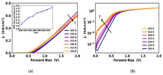
Figure 3.
(a) Temperature-dependent forward J-V characteristics on a linear scale (inset: differential specific on-resistance Ron,sp as a function of temperature T) and (b) in semi-log scale.
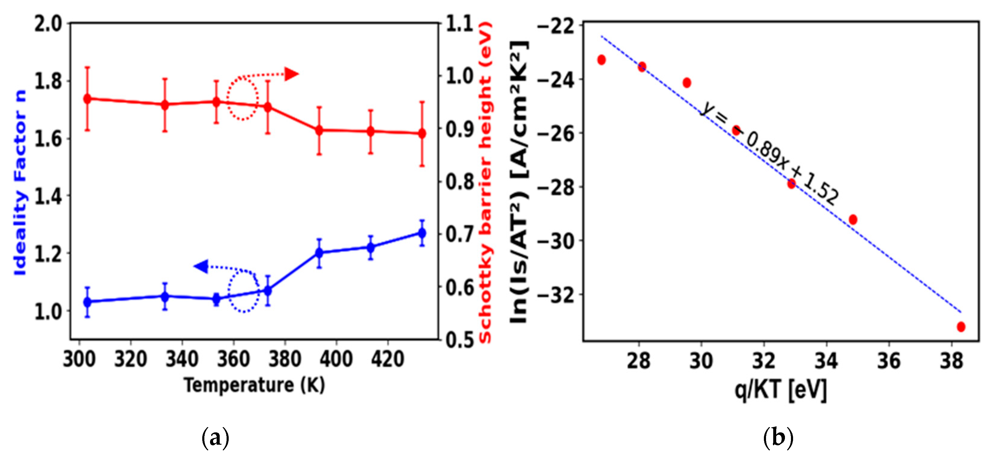
From Equation (2), from the intercept and the slope of the linear region of the ln (J)-V plot, and n can be determined, respectively. In Figure 4a, the ideality factor n of several devices increases from 1 to ~1.3 ± 0.05 at higher temperatures, which may indicate the impact of the surface traps on device performance [20]; the extracted n suggests that the thermionic emission (TE) dominates the current transport mechanism at low temperatures (from 300 K to 375K) and the thermionic field emission (TFE) at higher temperatures (T > 375 K). The variation in the barrier height when the temperature is between 375 and 425 K, as shown in Figure 4a, confirms the impact of traps on the Ni/GaN interface. These results suggest the thermal instability of the Schottky barrier height of the SBD at high temperatures [20,21].
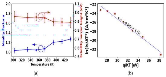
Figure 4.
(a) The extracted ideality factor n and Schottky barrier height as a function of temperature for several measured devices, and (b) the experimental Richardson’s plot.
From the calculations and as illustrated in Figure 4b, the experimental Richardson’s constant for several devices was determined from the intercept of the linear fitting of Equation (2) of 4.6 ± 0.7 A cm−2 K−2. It is suggested that the discrepancy from the theoretical value of 26.64 A K−2 cm−2 is due to the epitaxy’s quality and inhomogeneity in the barrier [22].
3.2. Reverse Bias
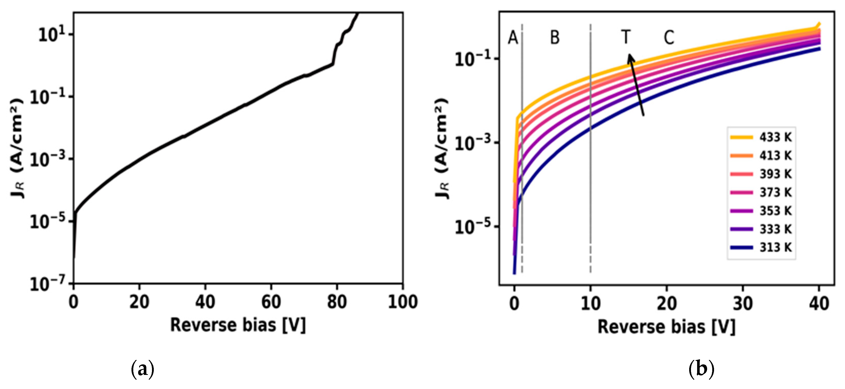
Figure 5a shows the typical reverse J-V characteristics of the GaN pseudo-vertical SBD. The destructive breakdown voltage (BV) of the Schottky barrier diode is around 80 V; this low voltage capability is mainly related to the absence of edge termination [17,18], and in particular is due to the expected high electric field at the edges of the Schottky contact.
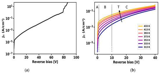
Figure 5.
(a) Typical breakdown characteristic of the fabricated pseudo-vertical GaN and (b) typical temperature-dependent reverse J–V characteristics on the log scale.
Leakage current in vertical devices has typically been associated with defects in the active layers since the dislocation density is high [11,23], in particular for GaN on Si devices.
The leakage current in Schottky barrier diodes (SBDs) can originate from two main sources: (1) electrodes—they have limited conduction mechanisms for which they are based on the electrical properties at the interface between the electrode and the semiconductor; (2) bulk-limited conduction mechanisms (also known as transport-limited conduction mechanisms)—they depend solely on the properties of the semiconductor material itself.
It is crucial to distinguish between these mechanisms, as several conduction processes can contribute simultaneously to current flow through the GaN drift layer. Performing temperature-dependent conduction current measurements can provide insights to reveal the origin of these currents, given that different mechanisms respond differently to temperature changes. The electrode-limited conduction mechanisms encompass (1) thermionic emission, _TE; (2) Fowler–Nordheim tunneling, _FNT; (3) direct tunneling or field emission, _FE; and (4) thermionic field emission, _TFE. On the other hand, the bulk-limited conduction mechanisms include (1) Frenkel–Poole emission, _FPE; (2) hopping conduction; (3) space-charge-limited conduction, _SCLC; (4) ohmic conduction; and (5) grain-boundary-limited conduction [16].
To study the reverse leakage mechanisms, the temperature dependence of reverse J-V for Ni/Au SBDs was measured from 313 to 433 K with a voltage range up to −40 V, as presented in Figure 5b. The characteristics can be categorized into three distinct voltage regions. Region “A” represents near-zero bias, region “B” represents bias from −1 to −10 V and region “C” is bias from −10 to −40 V. For Schottky devices under a reverse regime, the voltage is sustained across the drift region, forming a depletion layer, with the highest electric field situated at the metal–semiconductor contact. The breakdown voltage is restricted by breakdown at the edges. Edge terminations are necessary to reduce the electric field at their location, leading to behavior closer to parallel-plane breakdown.
Table 1 summarizes only the possible current mechanisms and the temperature and electric field dependencies of Schottky barrier diodes (SBDs) grown with localized epitaxy. Many process were excluded as most of the already-reported investigations for GaN on Si devices are focused on few mechanisms, such as thermionic emission (TE), Frenkel–Poole emission (FPE), variable range hopping (VRH) and finally trapped or phonon-assisted tunneling (TAT, PAT) [16].

Table 1.
Shows a summary of the possible leakage mechanisms for SBDs [24], where J is the current density, E is the electric field, Ec is the characteristic field, n is the ideality factor, T is the absolute temperature, k is the Boltzmann’s constant, is the trap energy level, is the relative dielectric constant of GaN, C is a constant, a is the localization radius of the electron wave function, T0 is the characteristic temperature and is the depletion width. The electric field can be obtained from the following expression.
In Region A, the leakage current seems to be limited by the Schottky contact, for which the conduction mechanism is dominated by Schottky emission. Electrons can gain sufficient energy by thermal excitation; electrons from the metal will overcome the Schottky barrier towards the conduction band. Figure 6 illustrates the Ni/n-GaN energy band diagram under negative bias. The most observed conduction process in Schottky barriers diodes (SBDs) is thermionic emission (TE).
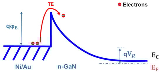
Figure 6.
Schematic energy band diagram of thermionic emission in metal–semiconductor structure.
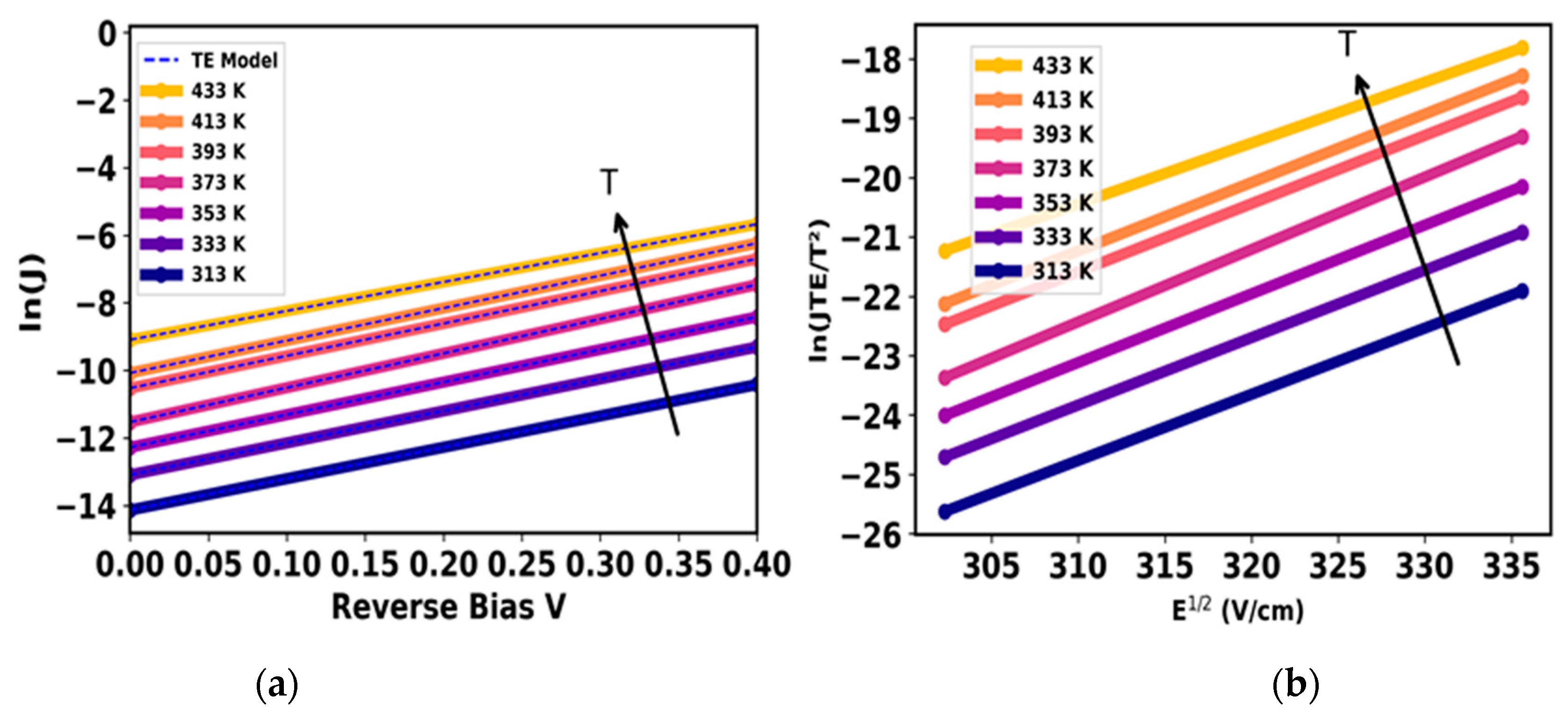
Figure 7a shows the reverse ln (J) versus V obtained at different temperatures at voltages from 0 to −0.4 V. The good fit between the experimental data and the thermionic emission (TE) model suggests that TE is the main mechanism at near-zero bias with barrier lowering of (the barrier lowering due the image force phenomenon is called the Schottky effect). Furthermore, the linear relationship between ln (J/T2) and E1/2, as shown in Figure 7b, confirms the dominance of this mechanism in this region.

Figure 7.
(a) Typical reverse ln (J) versus V with the fitting model and (b) ln (JTE/T2) versus E½ at the voltage range of 0 to −0.4 V.
In Region B, by increasing the reverse bias, the leakage current increases with temperature as observed in Figure 5b. This can be caused by the Frenkel–Poole emission (FPE), which is a process similar to Schottky emission or thermionic emission (TE), involving the thermal excitation of electrons from Coulombic traps into the semiconductor’s conduction band. This similarity often leads to FPEs being referred to as internal Schottky emissions. In this context, when an electron is in a trap, the application of an electric field can lead to a reduction in the electron’s Coulomb potential energy. This reduction in potential energy will increase the probability of the thermal excitation of electrons from the trap to the conduction band. Figure 8 shows the schematic energy band diagram of the FP emission.
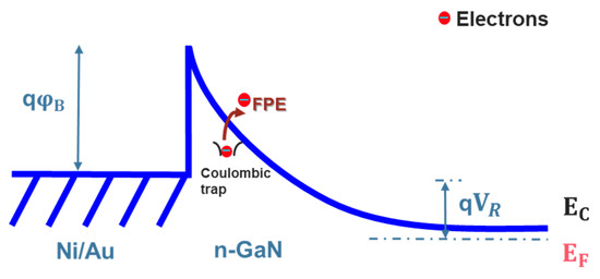
Figure 8.
Schematic energy band diagram of FP emission in metal–semiconductor structure.
According to the FPE equation, ln (J/E) should have a linear relationship with the square root of the electric field (note that the electric field (E) was calculated using Equation (3)) as shown in Figure 9, which indicates that FPE is the dominant leakage process in Region B.
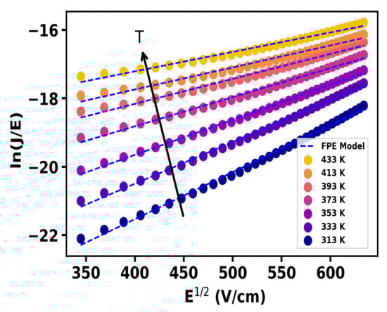
Figure 9.
Typical ln (J/E) versus fitted with FPE model in range voltage from 0.5 to 10 V.
In such a case, A(T) and B(T) are the intercept and slope of the ln (J/E) versus E1/2 plot and are defined as follows:
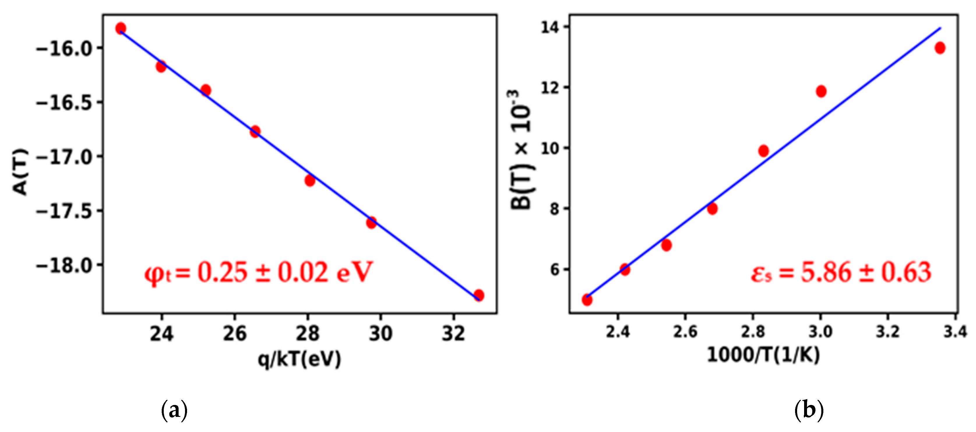
From Figure 10a, the trap level for FPE extracted from the linear fitting of Equation (4) is found at below the conduction band. They could possibly be related to nitrogen or gallium vacancies, VN − VGa, and nitrogen antisite NGa-related defects [28]. However, further experiments like characterization by deep level transient spectroscopy (DLTS) are needed to confirm these observed traps. In addition, the relative dielectric constant of GaN was extracted, from the linear fitting of Equation (5), as shown in Figure 10b. Furthermore, this was confirmed by the extracted Frenkel–Poole coefficient βFP of 3.13 × 10⁻⁴ eV V−1/2 cm1/2. These values are in good agreement with the reported values for GaN (5.4 and 7 × 10⁻⁴ eV V−1/2 cm1/2 for and βFP, respectively) [27,28], and confirm the domination of FPE in Region B with a voltage range of −0.5 to −10 V.
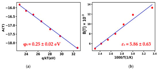
Figure 10.
(a) The slope of the ln (J/E) versus E1/2 A (T) as a function of . (b) The intercept B (T) as a function of 1000/T.
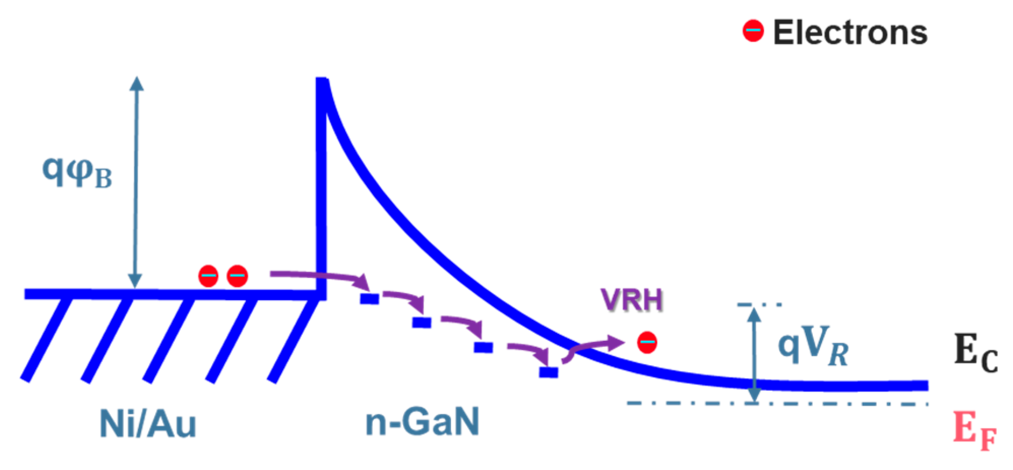
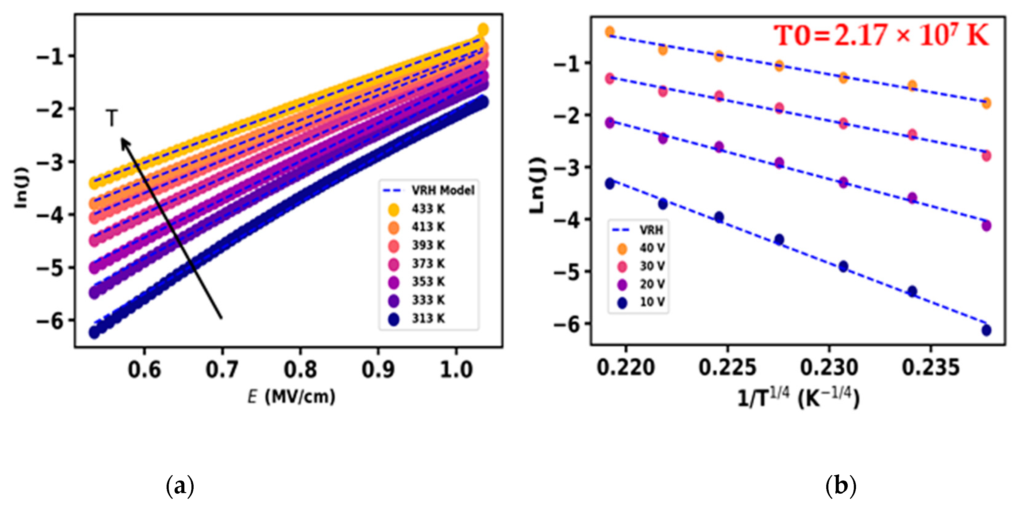
Finally, in Region C, when the reverse voltage increased up to −40 V with a corresponding electric field up to 1.1 MV/cm, the leakage current became insensitive to the temperature. This indicates that the reverse leakage is probably dominated by variable range hopping (VRH), for which the increased electric field distorts the energy band and makes it steeper. This results in a shorter hopping from the Schottky Fermi level and the VRH level in the GaN drift layer. Consequently, the hopping of electrons becomes easier from the Schottky metal to the GaN drift layer [29,30]. Figure 11 illustrates the schematic energy band diagram of the VRH mechanism.

Figure 11.
Schematic energy band diagram of VRH emission in metal–semiconductor structure.
The clear linear dependency between ln (J) and E is demonstrated, as shown in Figure 12a, suggesting the dominance of VRH. Figure 12b shows an Arrhenius plot of the reverse current at several voltages versus the inverse of the temperature. At a high electric field, the current has a lower temperature dependency and follows Mott’s law, [ln]. The extracted characteristic temperature T0 is 2.2 ± 1.1 × 10⁷ K, which is within the typical range of 106–109 K and is consistent with reported values in the literature (4.92 × 10⁷ for ND ~3 × 1016 cm−3) [31,32].

Figure 12.
(a) ln (J) as a function of applied electric field, E. (b) ln (J) versus (1/T)1/2 at reverse voltages of −10, −20, −30 and −40 V.
4. Discussion
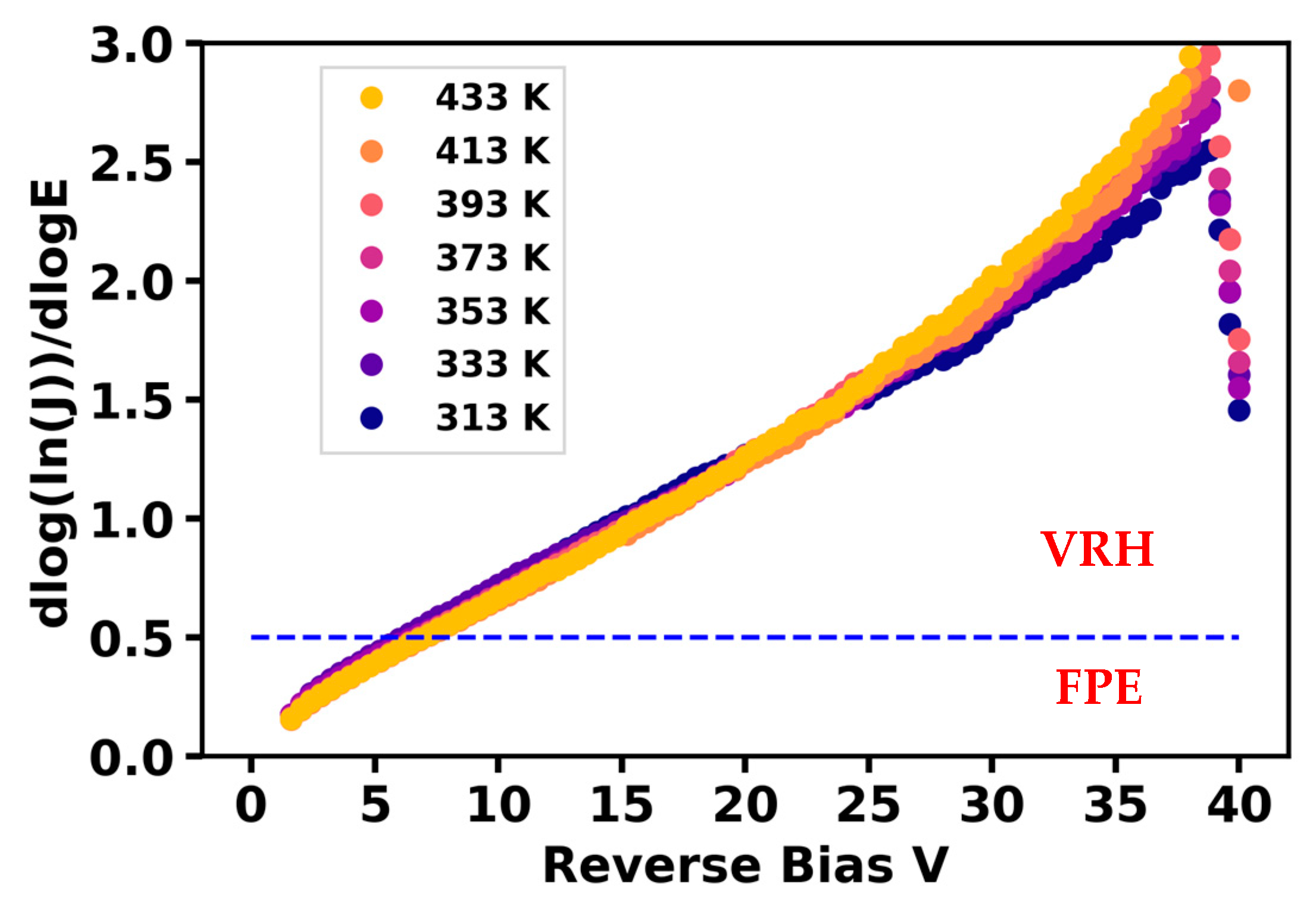
The investigated mechanisms were further confirmed by having the differential slope d[log(ln(J))]/dlog(E) as presented in Figure 13, where J is the current density and E is the applied electric field in the depletion region. When d[log(ln(J))]/dlog(E) is around 0.5, the Frenkel–Poole emission (FPE) process dominates the leakage current. On the other hand, if d [log (ln(J))]/dlog(E) is close to 1, the variable range hopping (VRH) is the mean leakage mechanism [25].

Figure 13.
d[log(ln(J))]/dlog(E) of GaN on Si SBD as function of applied voltage [25].
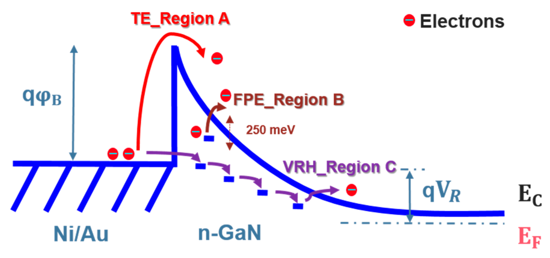
Figure 14 summarizes and illustrates the different leakage mechanisms revealed by temperature-dependent study of GaN-on-Si quasi-vertical SBDs grown by localized epitaxy. In Region A, thermionic emission (TE) dominates the leakage current since the applied voltage has a negligible impact on the Schottky barrier, in which electrons are transported from the metal to the n-GaN layer. As the bias increases, trapped electrons gain sufficient energy to surmount the trap state, which can be referred to as the Frenkel–Poole emission (FPE) process. Finally, in Region C, the increasing electric field reduces the hopping distance from the metal to trap states, which allows the electrons to hop easily from the Schottky metal to the conduction band of the GaN drift layer, which is referred to as variable range hopping (VRH). These leakage mechanisms are in agreement with previously reported studies for GaN devices [33,34,35].

Figure 14.
Schematic depicting determined leakage processes under reverse bias for GaN-on-Si SBD grown by localized epitaxy [28,33].
5. Conclusions
In this work, GaN-on-Si quasi-vertical Schottky barrier diodes (SBDs) were fabricated with Selective Area Growth (SAG). The SBDs achieved good forward performance, with a high current density of 2.5 kA/cm2, a low turn-on voltage of 0.6 V and an of 1.9 mΩ.cm2. A limited breakdown voltage of ~80 V was found, probably related to the absence of edge termination. Temperature-dependent reverse bias I–V characteristics in a range of 313–433 K were analyzed and the leakage current transport mechanisms were investigated. At near-zero bias (0 V to −0.5 V), the current density (J) follows a linear relationship with 1/T and the characteristics correspond to the thermionic emission (TE) leakage process. By increasing the reverse voltage up to −10 V, Frenkel–Poole emission (FPE) with an emission barrier of 0.25 becomes dominant. At higher voltages (−10 V to −40 V), the leakage current becomes insensitive to the temperature, which suggests that the variable range hopping (VRH) mechanism dominates. This work gives an in-depth insight into the leakage mechanisms and provides useful guidance to improve GaN vertical power devices on silicon substrates.
Author Contributions
Conceptualization, M.E.A., J.B., D.A., T.K., D.P.A., H.E.R. and M.C.; formal analysis, M.E.A.; funding acquisition, J.B. and M.C.; investigation, M.E.A., J.B. and D.A.; methodology, M.E.A.; project administration, J.B. and M.C.; resources, D.P.A. and H.E.R.; software, M.E.A. and J.B.; supervision, J.B. and D.A.; validation, J.B., D.A. and M.C.; visualization, M.E.A.; writing—original draft, M.E.A.; writing—review and editing, J.B., D.A. and M.C. All authors have read and agreed to the published version of the manuscript.
Funding
Agence Nationale de la Recherche: ANR-22-CE05-0010.
Data Availability Statement
Data are contained within the article.
Acknowledgments
This work is part of the ELEGaNT project (ANR-22-CE05-0010).
Conflicts of Interest
The authors declare no conflicts of interest.
References
- Dang, K.; Zhang, J.; Zhou, H.; Huang, S.; Zhang, T.; Bian, Z.; Zhang, Y.; Wang, X.; Zhao, S.; Wei, K.; et al. A 5.8-GHz High-Power and High-Efficiency Rectifier Circuit With Lateral GaN Schottky Diode for Wireless Power Transfer. IEEE Trans. Power Electron. 2020, 35, 2247–2252. [Google Scholar] [CrossRef]
- Chowdhury, S.; Stum, Z.; Li, Z.D.; Ueno, K.; Chow, T.P. Comparison of 600V Si, SiC and GaN Power Devices. Mater. Sci. Forum 2014, 778–780, 971–974. [Google Scholar]
- Langpoklakpam, C.; Liu, A.-C.; Hsiao, Y.-K.; Lin, C.-H.; Kuo, H.-C. Vertical GaN MOSFET Power Devices. Micromachines 2023, 14, 1937. [Google Scholar] [CrossRef] [PubMed]
- Zhang, Y.; Palacios, T. (Ultra)Wide-Bandgap Vertical Power FinFETs. IEEE Trans. Electron Devices 2020, 67, 3960–3971. [Google Scholar] [CrossRef]
- Baliga, B.J. Trends in power semiconductor devices. IEEE Trans. Electron Devices 1996, 43, 1717–1731. [Google Scholar] [CrossRef]
- Kachi, T. State-of-the-art GaN vertical power devices. In Proceedings of the 2015 IEEE International Electron Devices Meeting (IEDM), Washington, DC, USA, 7–9 December 2015; pp. 16.1.1-16.1.4. [Google Scholar]
- Hu, Z.; Nomoto, K.; Song, B.; Zhu, M.; Qi, M.; Pan, M.; Gao, X.; Protasenko, V.; Jena, D.; Xing, H.G. Near unity ideality factor and Shockley-Read-Hall lifetime in GaN-on-GaN p-n diodes with avalanche breakdown. Appl. Phys. Lett. 2015, 107, 243501. [Google Scholar] [CrossRef]
- Tanaka, N.; Hasegawa, K.; Yasunishi, K.; Murakami, N.; Oka, T. 50 A vertical GaN Schottky barrier diode on a free-standing GaN substrate with blocking voltage of 790 V. Appl. Phys. Express 2015, 8, 071001. [Google Scholar] [CrossRef]
- Guo, X.; Zhong, Y.; Zhou, Y.; Chen, X.; Yan, S.; Liu, J.; Sun, X.; Sun, Q.; Yang, H. 1200-V GaN-on-Si Quasi-Vertical p-n Diodes. IEEE Electron Device Lett. 2022, 43, 2057–2060. [Google Scholar] [CrossRef]
- Wei, Q.; Zhou, F.; Xu, W.; Ren, F.; Zhou, D.; Chen, D.; Zhang, R.; Zheng, Y.; Lu, H. Demonstration of Vertical GaN Schottky Barrier Diode With Robust Electrothermal Ruggedness and Fast Switching Capability by Eutectic Bonding and Laser Lift-Off Techniques. IEEE J. Electron Devices Soc. 2022, 10, 1003–1008. [Google Scholar] [CrossRef]
- Zou, X.; Zhang, X.; Lu, X.; Tang, C.W.; Lau, K.M. Breakdown Ruggedness of Quasi-Vertical GaN-Based p-i-n Diodes on Si Substrates. IEEE Electron Device Lett. 2016, 37, 1158–1161. [Google Scholar] [CrossRef]
- Zhang, Y.; Yuan, M.; Chowdhury, N.; Cheng, K.; Palacios, T. 720-V/0.35-m Ω·cm2 Fully Vertical GaN-on-Si Power Diodes by Selective Removal of Si Substrates and Buffer Layers. IEEE Electron Device Lett. 2018, 39, 715–718. [Google Scholar] [CrossRef]
- Tanaka, A.; Choi, W.; Chen, R.; Dayeh, S.A. Si Complies with GaN to Overcome Thermal Mismatches for the Heteroepitaxy of Thick GaN on Si. Adv. Mater. 2017, 29, 1702557. [Google Scholar] [CrossRef]
- Alquier, D.; Cayrel, F.; Menard, O.; Bazin, A.-E.; Yvon, A.; Collard, E. Recent Progresses in GaN Power Rectifier. Jpn. J. Appl. Phys. 2012, 51, 01AG08. [Google Scholar] [CrossRef]
- Kaltsounis, T.; Haas, H.; Lafossas, M.; Torrengo, S.; Maurya, V.; Buckley, J.; Mariolle, D.; Veillerot, M.; Gueugnot, A.; Mendizabal, L.; et al. Characterization of unintentional doping in localized epitaxial GaN layers on Si wafers by scanning spreading resistance microscopy. Microelectron. Eng. 2023, 273, 111964. [Google Scholar] [CrossRef]
- Zhang, Y.; Wong, H.Y.; Sun, M.; Joglekar, S.; Yu, L.; Braga, N.A.; Mickevicius, R.V.; Palacios, T. Design space and origin of off-state leakage in GaN vertical power diodes. In Proceedings of the 2015 IEEE International Electron Devices Meeting (IEDM), Washington, DC, USA, 7–9 December 2015; pp. 35.1.1-35.1.4. [Google Scholar] [CrossRef]
- Guo, X.; Zhong, Y.; Chen, X.; Zhou, Y.; Su, S.; Yan, S.; Liu, J.; Sun, X.; Sun, Q.; Yang, H. Reverse leakage and breakdown mechanisms of vertical GaN-on-Si Schottky barrier diodes with and without implanted termination. Appl. Phys. Lett. 2021, 118, 243501. [Google Scholar] [CrossRef]
- Maurya, V.; Buckley, J.; Alquier, D.; Irekti, M.-R.; Haas, H.; Charles, M.; Jaud, M.-A.; Sousa, V. Electrical Transport Characteristics of Vertical GaN Schottky-Barrier Diode in Reverse Bias and Its Numerical Simulation. Energies 2023, 16, 5447. [Google Scholar] [CrossRef]
- Sun, Y.; Kang, X.; Zheng, Y.; Lu, J.; Tian, X.; Wei, K.; Wu, H.; Wang, W.; Liu, X.; Zhang, G. Review of the Recent Progress on GaN-Based Vertical Power Schottky Barrier Diodes (SBDs). Electronics 2019, 8, 575. [Google Scholar] [CrossRef]
- Rhoderick, E.H.; Williams, R.H. Metal-Semiconductor Contacts; Clarendon Press: Oxford, UK, 1988; pp. 1–14. [Google Scholar]
- Chen, J.; Bian, Z.; Liu, Z.; Zhu, D.; Duan, X.; Wu, Y.; Jia, Y.; Ning, J.; Zhang, J.; Hao, Y. Effects of thermal annealing on the electrical and structural properties of Mo/Au schottky contacts on n-GaN. J. Alloys Compd. 2021, 853, 156978. [Google Scholar] [CrossRef]
- Phark, S.-H.; Kim, H.; Song, K.M.; Kang, P.G.; Shin, H.S.; Kim, D.-W. Current transport in Pt Schottky contacts to a-plane n-type GaN. J. Phys. Appl. Phys. 2010, 43, 165102. [Google Scholar] [CrossRef]
- Sang, L.; Ren, B.; Sumiya, M.; Liao, M.; Koide, Y.; Tanaka, A.; Cho, Y.; Harada, Y.; Nabatame, T.; Sekiguchi, T.; et al. Initial leakage current paths in the vertical-type GaN-on-GaN Schottky barrier diodes. Appl. Phys. Lett. 2017, 111, 122102. [Google Scholar] [CrossRef]
- Zhang, R.; Zhang, Y. Power device breakdown mechanism and characterization: Review and perspective. Jpn. J. Appl. Phys. 2023, 62, SC0806. [Google Scholar] [CrossRef]
- Simmons, J.G. Conduction in thin dielectric films. J. Phys. Appl. Phys. 1971, 4, 613. [Google Scholar] [CrossRef]
- Han, D.P.; Oh, C.H.; Kim, H.; Shim, J.I.; Kim, K.S.; Shin, D.S. Conduction Mechanisms of Leakage Currents in InGaN/GaN-Based Light-Emitting Diodes. IEEE Trans. Electron Devices 2015, 62, 587–592. [Google Scholar] [CrossRef]
- Peta, K.R.; Park, B.-G.; Lee, S.-T.; Kim, M.-D.; Oh, J.-E.; Kim, T.-G.; Reddy, V.R. Analysis of electrical properties and deep level defects in undoped GaN Schottky barrier diode. Thin Solid Films 2013, 534, 603–608. [Google Scholar] [CrossRef]
- Zhang, H.; Miller, E.J.; Yu, E.T. Analysis of leakage current mechanisms in Schottky contacts to GaN and Al0.25Ga0.75N∕GaN grown by molecular-beam epitaxy. J. Appl. Phys. 2006, 99, 023703. [Google Scholar] [CrossRef]
- Kuksenkov, D.V.; Temkin, H.; Osinsky, A.; Gaska, R.; Khan, M.A. Origin of conductivity and low-frequency noise in reverse-biased GaN p-n junction. Appl. Phys. Lett. 1998, 72, 1365–1367. [Google Scholar] [CrossRef]
- Chen, J.; Liu, Z.; Wang, H.; Song, X.; Bian, Z.; Duan, X.; Zhao, S.; Ning, J.; Zhang, J.; Hao, Y. Determination of the leakage current transport mechanisms in quasi-vertical GaN–on–Si Schottky barrier diodes (SBDs) at low and high reverse biases and varied temperatures. Appl. Phys. Express 2021, 14, 104002. [Google Scholar] [CrossRef]
- Look, D.C.; Reynolds, D.C.; Kim, W.; Aktas, Ö.; Botchkarev, A.; Salvador, A.; Morkoç, H. Deep-center hopping conduction in GaN. J. Appl. Phys. 1996, 80, 2960–2963. [Google Scholar] [CrossRef]
- Peta, K.R.; Kim, M.D. Leakage current transport mechanism under reverse bias in Au/Ni/GaN Schottky barrier diode. Superlattices Microstruct 2018, 113, 678–683. [Google Scholar] [CrossRef]
- Fu, K.; Fu, H.; Huang, X.; Yang, T.H.; Cheng, C.Y.; Peri, P.R.; Chen, H.; Montes, J.; Yang, C.; Zhou, J.; et al. Reverse Leakage Analysis for As-Grown and Regrown Vertical GaN-on-GaN Schottky Barrier Diodes. IEEE J. Electron Devices Soc. 2020, 8, 74–83. Available online: https://ieeexplore.ieee.org/abstract/document/8949530 (accessed on 1 May 2024). [CrossRef]
- Kwon, W.; Kawasaki, S.; Watanabe, H.; Tanaka, A.; Honda, Y.; Ikeda, H.; Iso, K.; Amano, H. Reverse Leakage Mechanism of Dislocation-Free GaN Vertical p-n Diodes. IEEE Electron Device Lett. 2023, 44, 1172–1175. [Google Scholar] [CrossRef]
- Rackauskas, B.; Dalcanale, S.; Uren, M.J.; Kachi, T.; Kuball, M. Leakage mechanisms in GaN-on-GaN vertical pn diodes. Appl. Phys. Lett. 2018, 112, 233501. [Google Scholar] [CrossRef]


Disclaimer/Publisher’s Note: The statements, opinions and data contained in all publications are solely those of the individual author(s) and contributor(s) and not of MDPI and/or the editor(s). MDPI and/or the editor(s) disclaim responsibility for any injury to people or property resulting from any ideas, methods, instructions or products referred to in the content. |
© 2024 by the authors. Licensee MDPI, Basel, Switzerland. This article is an open access article distributed under the terms and conditions of the Creative Commons Attribution (CC BY) license (https://creativecommons.org/licenses/by/4.0/).