Article

Coupling Response of Piezoelectric Semiconductor Composite Fiber under Local Temperature Change

1
Department of Mechanical and Automotive Engineering, Science and Technology College of Hubei, University of Arts and Science, Xiangyang 441025, China
2
School of Science, Lanzhou University of Technology, Lanzhou 730050, China
*
Author to whom correspondence should be addressed.
Crystals 2024, 14(7), 628; https://doi.org/10.3390/cryst14070628
Submission received: 13 May 2024 / Revised: 5 July 2024 / Accepted: 6 July 2024 / Published: 8 July 2024
(This article belongs to the Special Issue Advanced Ferroelectric, Piezoelectric and Dielectric Ceramics)

Abstract

:
This paper details the thermal–mechanical–electrical response of a piezoelectric semiconductor (PS) composite fiber composed of a PS layer and two piezoelectric layers under local temperature change. The phenomenological theory of thermal piezoelectric semiconductors (PSs) is adopted to obtain the analytical solution for each field in the composite fiber under local temperature change. Our findings reveal that such temperature fluctuations induce local polarization, leading to the formation of local potential barriers and potential wells that effectively impede the flow of low-energy electrons along the fiber. Furthermore, the initial carrier concentration and geometric parameters of the composite fiber exert significant influence on its individual fields. The results contribute to the structural design and practical application of piezoelectric semiconductor devices.

1. Introduction

PS materials, which possess both piezoelectric and semiconductor properties, have wide-ranging applications in electronics, sensors, and energy systems [1]. In recent years, nanostructures of PSs, including fiber, tubes, ribbons, and helices, fabricated from third-generation semiconductor materials like ZnO and AlN, have demonstrated a novel phenomenon termed the piezoelectric-electronics effect [2,3,4,5,6,7,8]. This effect refers to the phenomenon where mechanical stress or deformation impacts the behavior of electrons within piezoelectric materials. This effect involves the modulation of carrier-transport behavior by the piezoelectric field, offering innovative avenues for the design of novel piezoelectric semiconductor devices.
Various PS devices can be understood through coupled-field phenomenological theories [9,10], encompassing the linear piezoelectric theory, the charge-conservation theory of electrons and holes, and the drift-diffusion theory of semiconductors [11]. It is crucial to note that due to the inherent nonlinearity of the PS theory, the drift-current term defined as the product of unknown macroscopic electric fields and carrier concentrations plays a significant role [12]. This theory often assumes the nonlinear relationship between the applied mechanical, electrical, and thermal fields, and the resulting responses. The theoretical analysis of PS structures and devices is inherently interdisciplinary and spans multiple physics fields, from materials science to mechanics. This theory has found extensive application in addressing diverse issues within PSs, such as fiber extension [13,14,15,16,17] and bending [18,19,20,21], waves and vibrations [22,23,24,25,26,27,28,29], PN junctions [30,31,32], and cracking [33,34,35]. PSs are widely used to manufacture various sensors, including pressure sensors, accelerometers, and temperature sensors. They are also utilized as actuators, such as in piezoelectric ceramic actuators and piezoelectric motors. Additionally, PS energy harvesters can convert mechanical vibrations or stresses into electrical energy.
In the operational setting of PS structures, heating inevitably occurs, referred to as the thermal effect of PSs [36], which involves the coupling of the temperature field with other fields in the PSs. These fields tend to vary with temperature change. Temperature fluctuations are an unavoidable accompanying factor, either active or passive, and they invariably prompt carrier movement, thus necessitating thermal–mechanical–electrical coupling within the PS structure. The temperature variable is crucial for understanding the thermal activation processes within the PS materials. Temperature affects the mobility of charge carriers, the polarization behavior, and the interaction between the mechanical and electrical states of the material. Changes in any parameter trigger corresponding alterations in others. Most studies in this domain have been conducted under normal or room-temperature conditions, with little consideration given to the impact of temperature on PS nanostructures. Only a handful of literature sources have addressed this issue. The researchers aimed to study the coupled electromechanical behavior of PS fiber under different temperature conditions [37,38,39]. By developing a comprehensive model that considers the interaction between temperature, electric field, mechanical stress, and material properties, the study revealed how local temperature changes affect the piezoelectric and mechanical responses of the fiber. When there are local temperature fluctuations, various physical parameters within the PS structure alter, including displacement, potential, electrical displacement, polarization intensity, and carrier distribution. The response of PS composite optical fibers to local temperature changes involves multifield coupling effects.
Specifically, temperature variations induce polarization potentials that substantially modify the physical fields within PS structures through a series of coupling effects. For instance, research indicates that local temperature fluctuations can create localized barriers and potential wells within semiconductor composite fibers. The magnitude of these barriers or wells depends on the extent and area affected by the temperature change. Changes in local temperature induce alterations in the potential barriers and potential wells of the mechanical field within PS composite fibers, significantly impacting the performance and application of PS materials. This temperature variation directly influences the electronic potential barrier in the PS, thereby affecting the distribution of energy levels and electron mobility within the material. Variations in electron mobility directly impact the charge transport rate within the material. Hence, comprehending the relationship between the electronic potential barrier and temperature is crucial for optimizing the electronic structure design of PS materials, thereby enhancing their performance and stability in PS devices. In piezoelectric sensors and energy-harvesting devices, precise control and optimization of device performance can be achieved by adjusting the electronic potential barrier through temperature control. Precise modulation of local temperature changes allows for adjustments in the morphology and strength of the potential barriers and potential wells, thereby influencing the electronic structure and charge transport characteristics of the material. This regulation can enhance the sensitivity, response speed, and energy conversion efficiency of PS devices, offering more reliable and efficient solutions for various application scenarios. Therefore, investigating the thermomechanical coupling effect and its influence on carrier transport in composite PS optical fibers will advance the research into PSs and the development and application of new piezoelectric electronics and devices.
To address the aforementioned issues, this paper investigates the local modulation and response of PS composite fiber to temperature variations. It examines, in-depth, the impacts of semiconductor properties and geometric parameters on each fiber field under local temperature influences. The paper’s structure is as follows: Section 2 furnishes a comprehensive introduction to the core equations governing the thermal–mechanical–electrical coupling of PS fiber. Section 3 presents the establishment of a theoretical one-dimensional model equation for the expansion of PS composite fiber under local temperature change. Section 4 combines boundary and continuity conditions to derive the analytical solution for each fiber field affected by local temperature variations. Section 5 systematically investigates the electromechanical fields correlated with local temperature change and also explores the control mechanism of initial carrier concentration and geometric parameters of the electromechanical field. In conclusion, Section 6 provides the final insights and conclusions drawn from the study. The working mechanism is shown in Figure 1.

2. Basic Equations

The comprehensive three-dimensional (3D) phenomenological theory for PS materials, which encompasses the motion balance equation, Gauss’s law for electrostatic charge, and continuity equations for electrons and holes, can be expressed as [36,37]
T i j , j = ρ u ¨ i D i , i = q ( N D + n + p N A ) J i , i p = q p ˙ J i , i n = q n ˙
where i, j = 1, 2, 3. The stress component, mechanical displacement component, and electrical displacement component are denoted as Tij, ui, and Di, respectively. Tij represents the stress tensor components, where i and j are the indices denoting the directions of the stress components. ui denotes the displacement vector components, where i indicates the direction of displacement. Di symbolizes the electric displacement vector components, with i representing the direction. p is the hole concentration, J i p the hole current density, n the electron concentration, J i n the electron current density, N D + the concentrations of impurities of donors, and N A the concentrations of impurities of acceptors. The mass density, time variable, and elementary charge are denoted as ρ, t, and q. The constitutive relationship of PSs considering the pyroelectric effects are
S i j = s i j k l E T k l + d k i j E k + α i j θ D i = d i k l S k l + ε i k E E k + p i θ J i p = q p μ i j p E j q D i j p p , j J i n = q n μ i j n E j + q D i j n n , j
where Sij is the strain component, Ei the electric field component, s i j k l E the elastic compliance, dkij the piezoelectric constant, αij the thermal expansion coefficient, ε i k E the dielectric constant, and pi the pyroelectric constant. In the PS composite fiber, the higher piezoelectric constant dkij indicates the stronger coupling between mechanical and electrical states, leading to more efficient conversion between mechanical energy and electrical energy. The higher thermal expansion coefficient αij means that the material will experience more significant dimensional changes with temperature variations. The carrier mobilities are denoted as μ i j p and μ i j n . The carrier diffusion constants are denoted as D i j p and D i j n . From Equation (2)3,4, we learn that the current densities ( J i p and J i n ) comprise two components: the drift current ( q p μ i j p E j and q n μ i j n E j ) and the diffusion current ( q D i j p p , j and q D i j n n , j ). The nonlinear Equation (2)3,4 describe the drift currents of holes and electrons, respectively. These currents depend on the carrier concentration and electric field, which are yet to be determined. We consider the temperature θ to change uniformly. The Sij and Ei are
S i j = u i , j + u j , i 2 E i = φ , i
where φ represents the electric potential. We assume that the initial carrier concentrations are p 0 = N A and n 0 = N D + . The concentrations of carriers are given by
p = p 0 + Δ p n = n 0 + Δ n
where Δ n and Δ p represent perturbations of hole and electron concentrations, respectively. We only consider holes and electrons as small perturbations, i.e., Δ n and Δ p are much smaller than the initial concentrations p0 and n0. Therefore, we can linearize Equation (2)3,4 in the following equation:
J i p = q p 0 μ i j p E j q D i j p ( Δ p ) , j J i n = q n 0 μ i j n E j + q D i j n ( Δ n ) , j

3. 1D Model for Extension of Composite PS Fiber

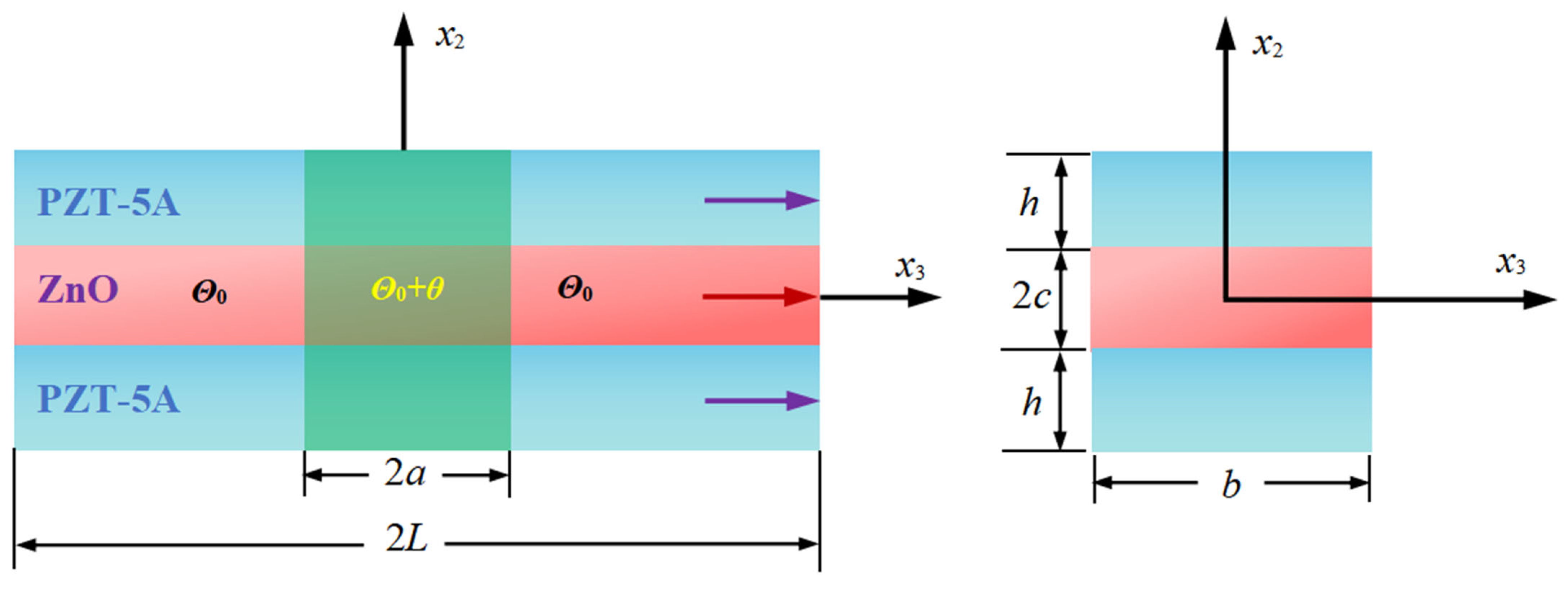
We consider the PS composite fiber depicted in Figure 2. The structure comprises a middle layer of PS (labeled “(I)”) sandwiched between two identical upper and lower piezoelectric layers (labeled “(II)”). Both the PS layer and the piezoelectric layer are polarized along the positive x3 axis. The temperature in the central region (|x3| < a) is Θ0 + θ, while in the other regions (|x3| > a), it remains Θ0. We investigate a layer of PS made of ZnO semiconductor material, with dimensions of 2L in length, 2c in thickness, and b in width. Each piezoelectric layer is made of PZT-5A material, measuring 2L in length, h in thickness, and b in width. For theoretical modeling convenience, we consider a very thin piezoelectric semiconductor composite fiber structure, where the length of the composite fiber is much larger than the characteristic dimension of its cross section. For the thin composite fiber, we use the common one-dimensional approximation that the axial displacement u and the potential φ depend only on the axial coordinate x3.
To model the extension of composite fiber, we approximate u3 and φ3 in the fiber as u 3 u 3 ( x 3 , t ) and φ 3 φ 3 ( x 3 , t ) . In the PS layer, we also make the following approximation as Δ n Δ n ( x 3 , t ) . Substituting into Equation (3), S33 and E3 are obtained as [38,39]
S 33 = u 3 , 3 E 3 = φ , 3
The stress relaxation of thin composite fiber is approximated as
T 11 T 22 0
Substituting Equation (7) into Equation (3) and solving for T33 and D3, we get
T 33 = c ¯ 33 S 33 e ¯ 33 E 3 λ ¯ 33 θ D 3 = e ¯ 33 S 33 + ε ¯ 33 E 3 + p ¯ 3 θ
where
c ¯ 33 = 1 / s 33 E       e ¯ 33 = d 33 / s 33 E λ ¯ 33 = α 33 / s 33 E ε ¯ 33 = ε 33 T d 33 2 / s 33 E p ¯ 3 = p 3 d 33 α 33 / s 33 E
The constitutive relationship of the electron current density J 3 n in Equation (5)2 is
J 3 n = q n 0 μ 33 n φ , 3 + q D 3 n ( Δ n ) , 3
For the PS layer, we obtain the 1D constitutive relation
T 33 = c ¯ 33 ( I ) S 33 e ¯ 33 ( I ) E 3 λ ¯ 33 ( I ) θ D 3 = e ¯ 33 ( I ) S 33 + ε ¯ 33 ( I ) E 3 + p ¯ 3 ( I ) θ
Similarly, for the piezoelectric layer, the 1D constitutive relationship between axial stress T33 and electric displacement D3 are
T 33 = c ¯ 33 ( I I ) S 33 e ¯ 33 ( I I ) E 3 λ ¯ 33 ( I I ) θ D 3 = e ¯ 33 ( I I ) S 33 + ε ¯ 33 ( I I ) E 3 + p ¯ 3 ( I I ) θ
By employing Equations (11) and (12), we can ascertain the total electric displacement ( D ^ ) and total force ( T ^ ) of the composite fiber cross-section:
T ^ = c ^ S 33 e ^ E 3 λ ^ θ D ^ = e ^ S 33 + ε ^ E 3 + p ^ θ
where
c ^ = c ¯ 33 ( I ) A ( I ) + c ¯ 33 ( I I ) A ( I I ) e ^ = e ¯ 33 ( I ) A ( I ) + e ¯ 33 ( I I ) A ( I I ) λ ^ = λ ¯ 33 ( I ) A ( I ) + λ ¯ 33 ( I I ) A ( I I ) ε ^ = ε ¯ 33 ( I ) A ( I ) + ε ¯ 33 ( I I ) A ( I I ) p ^ = p ¯ 3 ( I ) A ( I ) + p ¯ 3 ( I I ) A ( I I ) A ( I ) = 2 b c ,   A ( I I ) = 2 b h
For the axial extension deformation of the composite fiber, the 1D governing equations for the PS composite fiber are derived from Equation (1)1,2,4:
T ^ , 3 = 2 b ( ρ ( I ) c + ρ ( I I ) h ) u ¨ D ^ , 3 = q ( Δ n ) A ( I ) J 3 , 3 n = q ( Δ n ˙ )

4. Potential Barriers and Potential Wells Created by Local Temperature Change

In this section, we focus on n-type semiconductors, which contain significantly fewer holes than electrons. It can be assumed that p 0 . We assume that the system is static. As depicted in Figure 2, the fiber experiences a locally uniform temperature change, denoted by θ, within the region |x3| < a. At the ends of the composite fiber, where stress is zero and electrically open, the boundary conditions are given by
T ^ ( ± L ) = 0 J 3 n ( ± L ) = 0 D ^ ( ± L ) = 0
At the x3 = ±a interface for temperature change, the continuity condition has
u ( ± a ) = u ( ± a + ) n ( ± a ) = n ( ± a + ) φ ( ± a ) = φ ( ± a + ) T ^ ( ± a ) = T ^ ( ± a + ) D ^ ( ± a ) = D ^ ( ± a + ) J 3 n ( ± a ) = J 3 n ( ± a + )
The effective polarization charge density ρP and polarization intensity P3 can be expressed as
P 3 = D 3 ε 0 E 3 ρ P = P 3 , 3
When we consider that θ is small, we use Equation (15) to solve the regions within |x3| < a, −L < x3 < −a, and a < x3 < L. To simplify the calculation, we refer to reference [38] and consider the special case L = ∞. The results of the electric potential φ, displacement x3, and electron concentration perturbation Δn are
φ = { ( e ^ λ ^   +   p ^ c ^ ) k ( c ^ ε ^   +   e ^ 2 ) θ sinh ( k a ) e k x 3             < x 3 < a ( e ^ λ ^   +   p ^ c ^ ) k ( c ^ ε ^   +   e ^ 2 ) θ sinh ( k x 3 ) e k a                                         | x 3 | < a ( e ^ λ ^   +   p ^ c ^ ) k ( c ^ ε ^   +   e ^ 2 ) θ sinh ( k a ) e k x 3                     a < x 3 < +
u 3 = { e ^ c ^ ( e ^ λ ^   +   p ^ c ^ ) k ( c ^ ε ^   +   e ^ 2 ) θ sinh ( k a ) e k x 3                                                                                   < x 3 < a e ^ c ^ ( e ^ λ ^   +   p ^ c ^ ) k ( c ^ ε ^   +   e ^ 2 ) θ sinh ( k x 3 ) e k a   +   λ ^ θ c ^ ( x 3 + a )                                                 | x 3 | < a e ^ c ^ ( e ^ λ ^   +   p ^ c ^ ) k ( c ^ ε ^   +   e ^ 2 ) θ sinh ( k a ) e k x 3 + 2 λ ^ θ a c ^                                                           a < x 3 < +
Δ n = { k ( e ^ λ ^   +   p ^ c ^ ) q A ( 1 ) c ^ θ sinh ( k a ) e k x 3                     < x 3 < a k ( e ^ λ ^   +   p ^ c ^ ) q A ( 1 ) c ^ θ sinh ( k x 3 ) e k a                                                   | x 3 | < a k ( e ^ λ ^   +   p ^ c ^ ) q A ( 1 ) c ^ θ sinh ( k a ) e k x 3                               a < x 3 < +
where
k 2 = n 0 q μ 33 n D 3 n ε 33 T
The solutions for the other fields of the composite fiber are provided in Appendix A.

5. Numerical Results and Discussion

We consider PS fiber made of ZnO. The material parameters are taken from reference [9]: c ¯ 33 ( I ) = 211 GPa, ε ¯ 33 ( I ) = 8.85 × 10⁻¹¹ F/m, e ¯ 33 ( I ) = 1.32 C/m2, and mass density ρ = 5700 kg/m3. The pyroelectric constant p ¯ 3 ( I ) = −9.4 × 10⁻⁶ C/(m2·K), and thermal expansion coefficient α ¯ 33 ( I ) = 3.017 × 10⁻⁶ K−1 are from references [40,41]. At room temperature (T = 298 K), the diffusion constant can be calculated using the Einstein relation: D 33 n = μ 33 n κ B T / q , where κ B is the Boltzmann constant. We consider piezoelectric fiber made of PZT-5A. Elastic constant c ¯ 33 ( I I ) = 86.856 GPa, piezoelectric constant e ¯ 33 ( I I ) = 15.1 C/m2, dielectric constant ε ¯ 33 ( I I ) = 1.5 × 10⁻⁹ C2/(N·m2), mass density ρ = 7750 kg/m3, pyroelectric constant p ¯ 3 ( I I ) = −238 × 10−6 C/(m2·K), and thermal expansion coefficient α ¯ 33 ( I I ) = 3 × 10⁻⁶ K−1 are from references [42,43,44]. The physical dimensions are a = 1 µm, b = 100 nm, c = 15 nm, L = 10 µm, and h = 35 nm.

5.1. Effect of Local Temperature Change on PS Composite Fiber

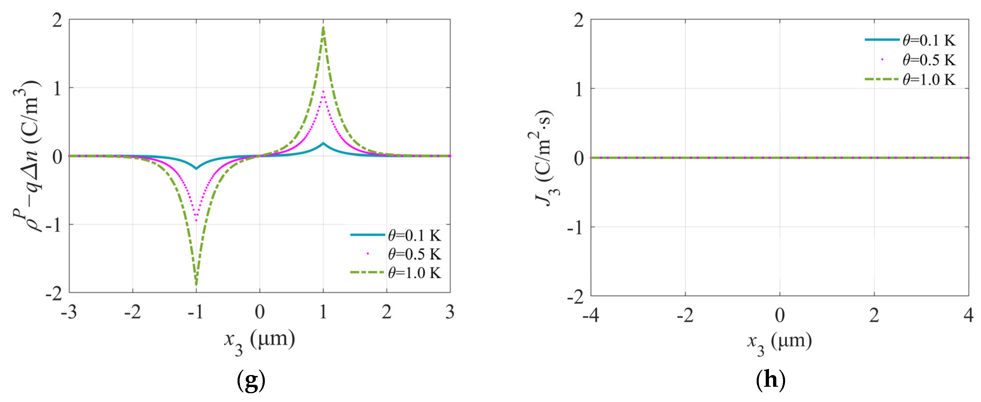
Equation (13)1 indicates that changes in local temperature θ lead to stress generation in the PS composite fiber. Similarly, Equation (13)2 demonstrates that alterations in local temperature θ result in electric displacement within the PS composite fiber. Thus, PS composite fiber manifests thermal–mechanical–electrical coupling effects in response to local temperature variations. Temperature change creates temperature gradients within the material, causing carrier redistribution and thus generating a potential difference. An increase in temperature increases the carrier concentration, forming a high potential region called a potential barrier. This high potential region hinders the free movement of carriers. Conversely, a decrease in temperature reduces the carrier concentration, forming a low potential region called a potential well, which attracts carriers. The specific values or ranges of potential barriers and potential wells induced by local temperature change in PS fibers are influenced by numerous factors, including material properties, temperature change amplitude and rate, and fiber structure. Due to the variability in materials and conditions, providing exact values or ranges is challenging. The depth of the potential barriers and potential wells hinges on the increase in carrier concentration in the high-temperature region and the material’s band structure. Generally, the depth of the potential barrier ranges from a few hundred millielectronvolts (meV) to a few thousand meV [36]. The depth of the potential well is similar to that of the potential barrier. Moreover, the depths of both the potential barriers and potential wells are proportional to the amplitude of the temperature change. A greater temperature change amplitude yields deeper potential barriers and potential wells. Figure 3 shows the impact of temperature change θ on various fields within the PS composite fiber, with an initial reference electron concentration of n0 = 1 × 10²¹ m−3. In Figure 3a, it is evident that local temperature change results in distinct potential barriers and potential wells, impeding the flow of electrons with low energy along the fiber. At the interface |x3| = 1 µm (the interface where the temperature undergoes an abrupt change), Figure 3b demonstrates an expected alteration in both positive and negative values of the potential. As shown in Figure 3a,b, local temperature change alters the carrier concentration, increasing it in high-temperature areas and decreasing it in low-temperature areas. This uneven distribution creates a potential difference and an electric field. Figure 3c illustrates how thermally induced local polarization leads to the formation of potential barriers and potential wells, as shown in Figure 3a. Equation (18)1 demonstrates that the product of the vacuum dielectric constant ε0 and the electric field E3 is minimal. Consequently, the polarization intensity P3 and the electric displacement D3 exhibit negligible variation. The variation in the electrical displacement (Figure 3d) is basically the same as that of the polarization intensity (Figure 3c). There is a significant change in the central region (temperature-change region) and zero at the ends of the composite fiber. As can be seen from Equation (18)2, ρP has an opposite sign to the reciprocal of the polarization intensity P3. The concentration of Δn in Figure 3e increases with increasing temperature, as expected. As illustrated in Figure 3g, the shielding effect of electrons results in the disturbance electron carrying a charge of −qΔn, while the effective polarization charge density ρP (also shown in Figure 3f) exhibits opposite signs. The charge carried by the disturbance electron −qΔn predominantly influences the system. As shown in Figure 3h, the electron charge density J 3 n in the PS composite fiber is zero. Since we are examining a static structure, we know from Equation (15)3 that J 3 n is a constant value. Additionally, the boundary condition given in Equation (16) for the numerical example indicates that J 3 n ( ± L ) = 0 . Therefore, in this scenario, the sum of the drift current q n 0 μ 33 n φ , 3 and the diffusion current q D 3 n ( Δ n ) , 3 in Equation (10) is zero. As can be seen in Figure 3, the different fields in the composite fiber are sensitive to temperature, and larger temperature changes produce stronger fields.

5.2. Effect of Initial Carrier Concentration on PS Composite Fiber

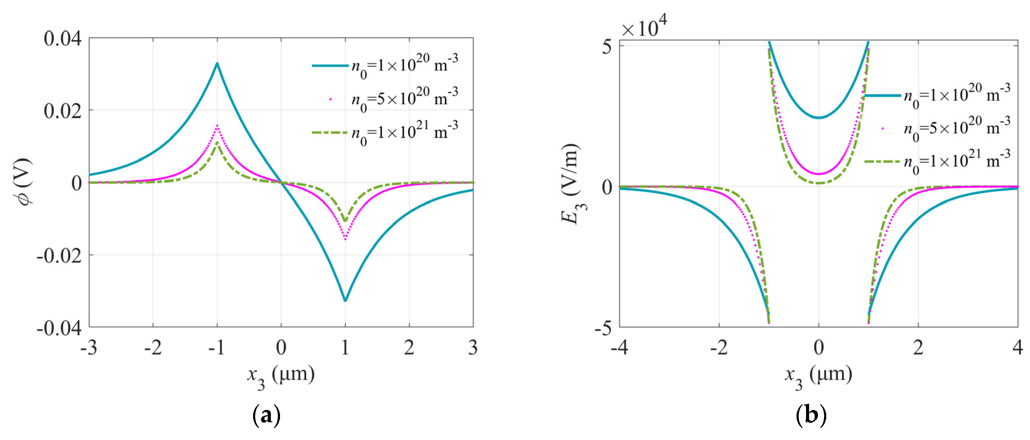
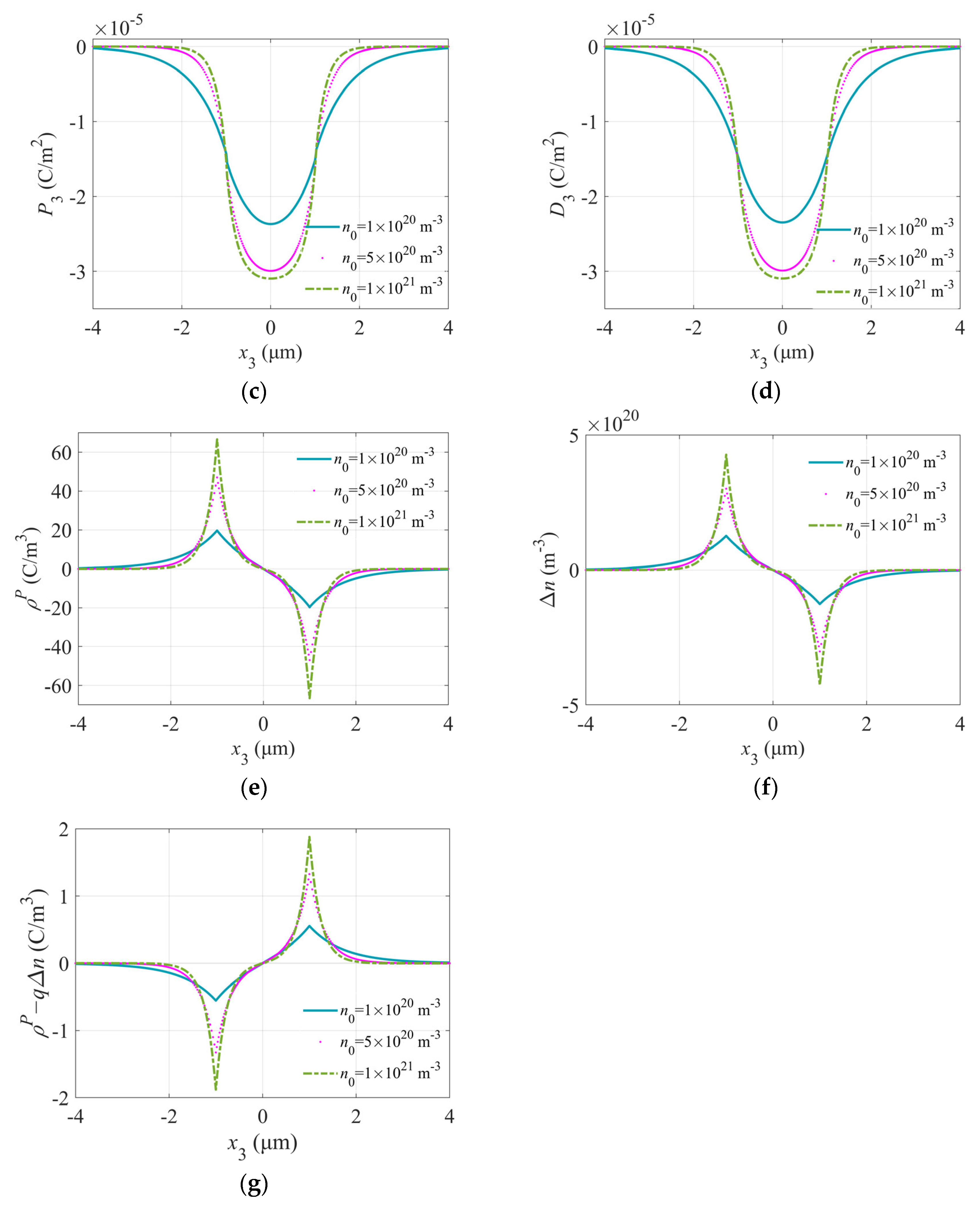
Figure 4 depicts the impact of various initial carrier concentrations (n0 = 1 × 10²⁰ m−3, 5 × 10²⁰ m−3, and 1 × 10²¹ m−3) on the identical fields shown in Figure 3, when θ = 1 K. It is evident that different fields within the composite fiber demonstrate sensitivity to n0. Figure 4a,b indicate that due to the shielding effect of mobile charges, the displacement and electric field of the composite piezoelectric fiber increase as n0 decreases. Figure 4c,d demonstrate that the intensity of thermally induced polarization and electric displacement increases with the rise in n0. Local temperature change generates numerous electromechanical fields, a situation akin to the phenomenon observed in a single PS fiber, as discussed in references [37,38,39]. Incorporating piezoelectric fibers into composite materials enhances their overall thermal stability. Piezoelectric fibers typically exhibit superior thermal stability, ensuring more consistent performance amid temperature fluctuations, and mitigating performance degradation resulting from localized temperature changes. As depicted in Figure 4c,d, local temperature fluctuations induce potential wells in the polarization intensity and electric displacement within the PS fiber. Higher carrier concentrations result in deeper potential wells. The polarized charge ρP and electron concentration disturbance Δn under different n0 conditions also escalate with n0, as depicted in Figure 4e,f. Similar to Figure 3, the perturbed electrons carry charge −qΔn of opposite sign to the polarized charge ρP, as evidenced in Figure 4e,g. As demonstrated in Equations (18)–(21), n0 is intricately linked to the individual fields.
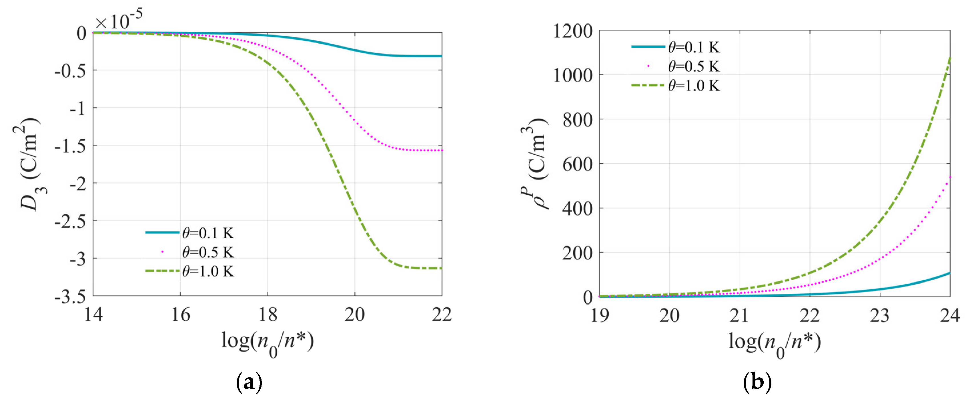
Figure 5 shows the variation in the electric displacement and effective polarization charge density of the composite fiber with the dimensionless initial carrier concentration n0/n* (n* = 1 m−3) at different temperature changes. As seen in Figure 5a, when n0 is between 1015 m−3 and 1021 m−3, the electric displacement drops sharply, exhibiting clear semiconductor characteristics (at x3 = 0 μm). When n0 is less than 1015 m−3, the initial carrier concentration is low, and the fiber exhibits piezoelectric properties. When n0 exceeds 1021 m−3, the initial carrier concentration is high, and the electric displacement stabilizes at a fixed value. The effect of the initial carrier concentration on the electric displacement is significant in the range of approximately 1015 m−3 to 1021 m−3. As shown in Figure 5b, when n0 is less than 1020 m−3, the effective polarization charge density is low (at x3 = −1 μm). When n0 exceeds 1020 m−3, the effective polarization charge density increases sharply. This result is consistent with the findings in Figure 4e,f.

5.3. Effect of the Geometrical Parameters on PS Composite Fiber

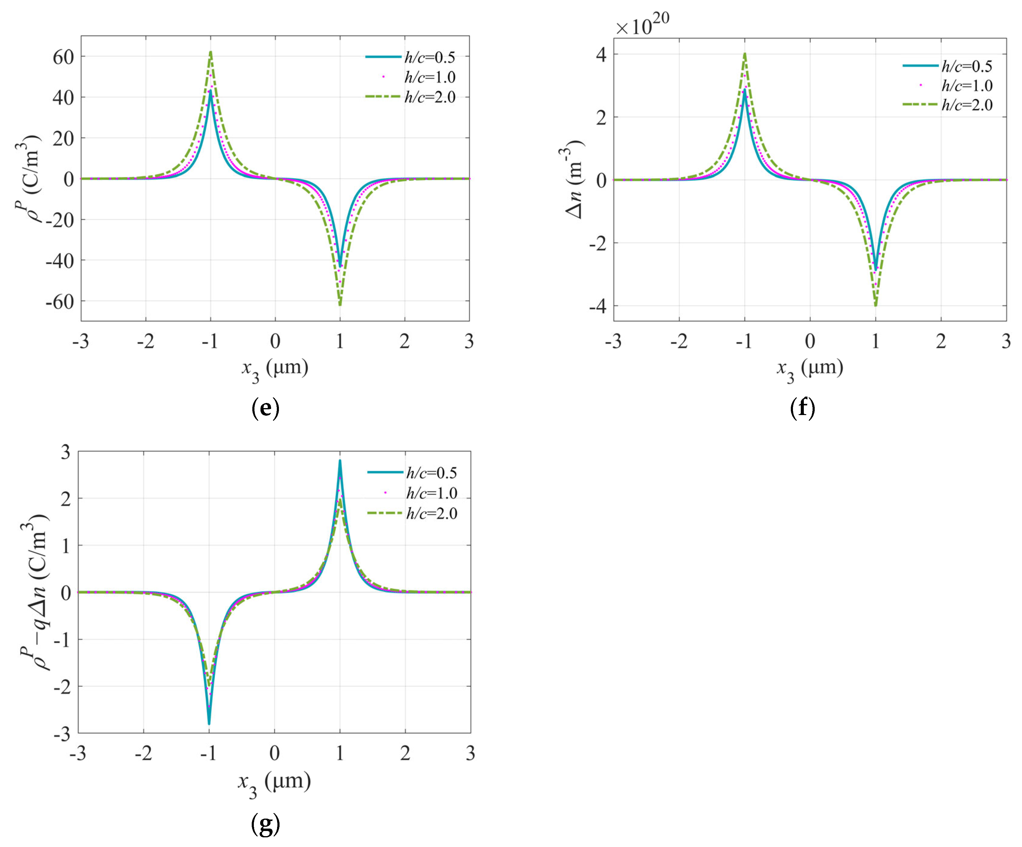
To gain a deeper insight into how the geometrical parameters of the composite fiber influence the tuning of the various fields induced by the localized heat of the PS, we plot the distribution of the different h/c (h/c = 0.5, 1, and 2) in Figure 6, when θ = 1 K and n0 = 1 × 10²¹ m−3. As can be seen in Figure 6, for different fields in the composite fiber, the larger the h/c, the stronger the field.
The multilayer design of piezoelectric semiconductor composite fibers optimizes the synergistic performance of piezoelectric and semiconductor properties, enhancing overall response characteristics. This design mitigates stress and deformation due to temperature fluctuations, ensuring stable electrical and mechanical properties. Functional integration allows composite fibers to maintain stable performance across varying temperatures, broadening their applications in electronics, optics, and mechanics. Investigating the microscopic mechanisms under local temperature changes, including charge transfer, polarization behavior, and stress distribution, offers new insights into the behavior of piezoelectric and semiconductor materials in complex environments. Exploring applications of new piezoelectric and semiconductor materials can further enhance composite fiber performance, advancing materials science and engineering technology. These studies not only innovate in structural design and functional integration but also drive advancements and applications in related fields.

6. Conclusions

Drawing from the phenomenological theory of thermal piezoelectric semiconductors, this study delves into the coupled thermal–mechanical–electrical effects of piezoelectric semiconductor composite fiber under localized temperatures. Analytical solutions for each field are derived, alongside an examination of the impact on carriers within piezoelectric semiconductors under localized temperature conditions. Furthermore, the study explores the influence of semiconductor properties and geometrical parameters of the composite fiber on each field. Finally, some qualitative conclusions are drawn, as follows:
(1)
Local temperature change can cause local polarization of piezoelectric semiconductor composite optical fiber. This, in turn, generates localized potentials and barrier wells, effectively hindering the flow of low-energy electrons along the fiber. Various fields within the composite fiber exhibit sensitivity to temperature, with greater temperature variations resulting in stronger fields. At interfaces where abrupt temperature changes occur, significant positive and negative shifts in potential are observed.
(2)
Both the initial carrier concentration and the geometrical parameters of the composite fiber significantly influence the individual fields within it, offering the potential for effective regulation. Consequently, the variation in local temperature acts akin to a diode, enabling effective control over electron flow through potential barriers and wells.
In summary, the findings presented in this paper serve as a valuable theoretical framework for precisely characterizing the impact of local temperature fluctuations on the physical and mechanical properties of composite semiconductor fiber, thereby enhancing our understanding of the underlying mechanisms. The quantitative results derived from these calculations provide essential insights for guiding the structural design and practical utilization of PS devices.

Author Contributions

Conceptualization, C.L.; methodology, W.W.; formal analysis, C.L.; investigation, C.L. and W.W.; data curation, C.L.; writing—original draft preparation, C.L.; writing—review and editing, W.W.; visualization, C.L.; funding acquisition, C.L. All authors have read and agreed to the published version of the manuscript.

Funding

This research was funded by Scientific Research Plan Project of Hubei Provincial Department of Education, grant number B2021455.

Data Availability Statement

The original contributions presented in the study are included in the article, further inquiries can be directed to the corresponding author.

Conflicts of Interest

The authors declare no conflicts of interest.

Appendix A

The results of the strain S3, electric field E3, electric displacement D3, polarization intensity P3, effective polarization charge density ρP, total charge density ρPqΔn, and electron current density J 3 n are
S 3 = { e ^ c ^ ( e ^ λ ^   +   p ^ c ^ ) ( c ^ ε ^   +   e ^ 2 ) θ sinh ( k a ) e k x 3                                         < x 3 < a e ^ c ^ ( e ^ λ ^   +   p ^ c ^ ) ( c ^ ε ^   +   e ^ 2 ) θ cosh ( k x 3 ) e k a + λ ^ θ c ^                                   | x 3 | < a e ^ c ^ ( e ^ λ ^   +   p ^ c ^ ) ( c ^ ε ^   +   e ^ 2 ) θ sinh ( k a ) e k x 3                                             a < x 3 < +
E 3 = { e ^ λ ^   +   p ^ c ^ c ^ ε ^   +   e ^ 2 θ sinh ( k a ) e k x 3                                         < x 3 < a e ^ λ ^   +   p ^ c ^ c ^ ε ^   +   e ^ 2 θ cosh ( k x 3 ) e k a                                                           | x 3 | < a e ^ λ ^   +   p ^ c ^ c ^ ε ^   +   e ^ 2 θ sinh ( k a ) e k x 3                                                   a < x 3 < +
D 3 = { ( e ^ λ ^   +   p ^ c ^ ) c ^ A ( 1 ) θ sinh ( k a ) e k x 3                                                                   < x 3 < a ( e ^ λ ^   +   p ^ c ^ ) c ^ A ( 1 ) θ cosh ( k x 3 ) e k a   +   ( e ^ λ ^   +   p ^ c ^ ) c ^ A ( 1 ) θ                                     | x 3 | < a ( e ^ λ ^   +   p ^ c ^ ) c ^ A ( 1 ) θ sinh ( k a ) e k x 3                                                                       a < x 3 < +
P 3 = { ( 1 c ^ A ( 1 ) ε 0 c ^ ε ^   +   e ^ 2 ) ( e ^ λ ^ + p ^ c ^ ) θ sinh ( k a ) e k x 3                                                                 < x 3 < a ( 1 c ^ A ( 1 ) ε 0 c ^ ε ^   +   e ^ 2 ) ( e ^ λ ^ + p ^ c ^ ) θ cosh ( k x 3 ) e k a   +   ( e ^ λ ^   +   p ^ c ^ ) c ^ A ( 1 ) θ                                   | x 3 | < a ( 1 c ^ A ( 1 ) ε 0 c ^ ε ^   +   e ^ 2 ) ( e ^ λ ^ + p ^ c ^ ) θ sinh ( k a ) e k x 3                                                                           a < x 3 < +
ρ P = { ( 1 c ^ A ( 1 ) ε 0 c ^ ε ^   +   e ^ 2 ) ( e ^ λ ^ + p ^ c ^ ) k θ sinh ( k a ) e k x 3                                         < x 3 < a ( 1 c ^ A ( 1 ) ε 0 c ^ ε ^   +   e ^ 2 ) ( e ^ λ ^ + p ^ c ^ ) k θ sinh ( k x 3 ) e k a                                                                           | x 3 | < a ( 1 c ^ A ( 1 ) ε 0 c ^ ε ^   +   e ^ 2 ) ( e ^ λ ^   +   p ^ c ^ ) k θ sinh ( k a ) e k x 3                                                     a < x 3 < +
ρ P q Δ n = { ε 0 ( e ^ λ ^   +   p ^ c ^ ) c ^ ε ^   +   e ^ 2 k θ sinh ( k a ) e k x 3                                         < x 3 < a ε 0 ( e ^ λ ^   +   p ^ c ^ ) c ^ ε ^   +   e ^ 2 k θ sinh ( k x 3 ) e k a                                                         | x 3 | < a ε 0 ( e ^ λ ^   +   p ^ c ^ ) c ^ ε ^   +   e ^ 2 k θ sinh ( k a ) e k x 3                                             a < x 3 < +
J 3 n = { ( q n 0 μ 33 n c ^ ε ^   +   e ^ 2 D 3 n k 2 A ( 1 ) c ^ ) ( e ^ λ ^ + p ^ c ^ ) θ sinh ( k a ) e k x 3                                         < x 3 < a ( q n 0 μ 33 n c ^ ε ^   +   e ^ 2 + D 3 n k 2 A ( 1 ) c ^ ) ( e ^ λ ^ + p ^ c ^ ) θ cosh ( k x 3 ) e k a                                                           | x 3 | < a ( q n 0 μ 33 n c ^ ε ^   +   e ^ 2 D 3 n k 2 A ( 1 ) c ^ ) ( e ^ λ ^ + p ^ c ^ ) θ sinh ( k a ) e k x 3                                             a < x 3 < +

References

  1. Wang, Z.L.; Wu, W.Z.; Falconi, C. Piezotronics and piezophototronics with third generation semiconductors. MRS Bull. 2018, 43, 922–927. [Google Scholar] [CrossRef]
  2. Zhang, Y.; Leng, Y.; Willatzen, M.; Huang, B. Theory of piezotronics and piezophototronics. MRS Bull. 2018, 43, 928–935. [Google Scholar] [CrossRef]
  3. Wang, C.; Bao, R.; Zhao, K.; Zhang, T.; Dong, L.; Pan, C. Enhanced emission intensity of vertical aligned flexible ZnO nanowire/p-polymer hybridized LED array by piezophototronic effect. Nano Energy 2015, 14, 364–371. [Google Scholar] [CrossRef]
  4. Wang, X.; Peng, W.; Yu, R.; Zou, H.; Dai, Y.; Zi, Y.; Wu, C.; Li, S.; Wang, Z.L. Simultaneously enhancing light emission and suppressing efficiency droop in GaN microwire-based ultraviolet light-emitting diode by the piezo-phototronic effect. Nano Lett. 2017, 17, 3718–3724. [Google Scholar] [CrossRef] [PubMed]
  5. Zhu, L.; Wang, L.; Xue, F.; Chen, L.; Fu, J.; Feng, X.; Li, T.; Wang, Z.L. Piezophototronic effect enhanced flexible solar cells based on n-ZnO/p-SnS core-shell nanowire array. Adv. Sci. 2017, 4, 1600185. [Google Scholar] [CrossRef]
  6. Zhu, L.; Zhang, Y.; Lin, P.; Wang, Y.; Yang, L.; Chen, L.; Wang, L.; Chen, B.; Wang, Z.L. Piezotronic effect on Rashba spin-orbit coupling in a ZnO/P3HT nanowire array structure. ACS Nano 2018, 12, 1811–1820. [Google Scholar] [CrossRef] [PubMed]
  7. Wang, L.; Liu, S.; Zhang, Z.; Feng, X.; Zhu, L.; Guo, H.; Ding, W.; Chen, L.; Qin, Y.; Wang, Z.L. 2D piezotronics in atomically thin zinc oxide sheets: Interfacing gating and channel width gating. Nano Energy 2019, 60, 724–733. [Google Scholar] [CrossRef]
  8. Qu, Y.L.; Pan, E.; Zhu, F.; Roy, A.K. Modeling thermoelectric effects in piezoelectric semiconductors: New fully coupled mechanisms for mechanically manipulated heat flux and refrigeration. Int. J. Eng. Sci. 2023, 180, 103775. [Google Scholar] [CrossRef]
  9. Auld, B.A. Acoustic Fields and Waves in Solids; John Wiley and Sons: New York, NY, USA, 1973; Volume I. [Google Scholar]
  10. Pierret, R.F. Semiconductor Fundamentals, 2nd ed.; Addison-Wesley: Boston, MA, USA, 1988. [Google Scholar]
  11. Yang, G.Y.; Du, J.K.; Wang, J.; Yang, J.S. Extension of a piezoelectric semiconductor fiber with consideration of electrical nonlinearity. Acta Mech. 2018, 229, 4663–4676. [Google Scholar] [CrossRef]
  12. Guo, M.K.; Li, Y.; Qin, G.S.; Zhao, M.H. Nonlinear solutions of PN junctions of piezoelectric semiconductors. Acta Mech. 2019, 230, 1825–1841. [Google Scholar] [CrossRef]
  13. Zhang, C.; Wang, X.; Chen, W.; Yang, J. An analysis of the extension of a ZnO piezoelectric semiconductor fiber under an axial force. Smart Mater. Struct. 2017, 26, 25030. [Google Scholar] [CrossRef]
  14. Araneo, R.; Lovat, G.; Burghignoli, P.; Falconi, C. Piezo-semiconductive quasi-1D nanodevices with or without anti-symmetry. Adv. Mater. 2012, 24, 4719–4724. [Google Scholar] [CrossRef] [PubMed]
  15. Wang, G.; Liu, J.; Liu, X.; Feng, W.; Yang, J. Extensional vibration characteristics and screening of polarization charges in a ZnO piezoelectric semiconductor fiber. J. Appl. Phys. 2018, 124, 094502. [Google Scholar] [CrossRef]
  16. Yang, W.; Hu, Y.; Yang, J. Transient extensional vibration in a ZnO piezoelectric semiconductor fiber under a suddenly applied end force. Materials Research Express. 2018, 6, 025902. [Google Scholar] [CrossRef]
  17. Huang, H.; Qian, Z.; Yang, J. IV characteristics of a piezoelectric semiconductor nanofiber under local tensile/compressive stress. J. Appl. Phys. 2019, 126, 164902. [Google Scholar] [CrossRef]
  18. Gao, Y.; Wang, Z.L. Electrostatic potential in a bent piezoelectric nanowire. The fundamental theory of nanogenerator and nanopiezotronics. Nano Lett. 2007, 7, 2499–2505. [Google Scholar] [CrossRef] [PubMed]
  19. Gao, Y.; Wang, Z.L. Equilibrium potential of free charge carriers in a bent piezoelectric semiconductive nanowire. Nano Lett. 2009, 9, 1103–1110. [Google Scholar] [CrossRef] [PubMed]
  20. Fan, S.; Liang, Y.; Xie, J.; Hu, Y. Exact solutions to the electromechanical quantities inside a statically-bent circular ZnO nanowire by taking into account both the piezoelectric property and the semiconducting performance: Part I–Linearized analysis. Nano Energy 2017, 40, 82–87. [Google Scholar] [CrossRef]
  21. Dai, X.; Zhu, F.; Qian, Z.; Yang, J. Electric potential and carrier distribution in a piezoelectric semiconductor nanowire in time-harmonic bending vibration. Nano Energy 2018, 43, 22–28. [Google Scholar] [CrossRef]
  22. Wauer, J.; Suherman, S. Thickness vibrations of a piezo-semiconducting plate layer. Int. J. Eng. Sci. 1997, 35, 1387–1404. [Google Scholar] [CrossRef]
  23. Li, P.; Jin, F.; Yang, J. Effects of semiconduction on electromechanical energy conversion in piezoelectrics. Smart Mater. Struct. 2015, 24, 025021. [Google Scholar] [CrossRef]
  24. Gu, C.; Jin, F. Shear-horizontal surface waves in a half-space of piezoelectric semiconductors. Philos. Mag. Lett. 2015, 95, 92–100. [Google Scholar] [CrossRef]
  25. Yang, L.; Zappino, E.; Carrera, E.; Du, J. Shear horizontal waves in a multiferroic composite semiconductor structure. Ultrasonics 2024, 139, 107287. [Google Scholar] [CrossRef] [PubMed]
  26. Jiao, F.; Wei, P.; Zhou, Y.; Zhou, X. Wave propagation through a piezoelectric semiconductor slab sandwiched by two piezoelectric half-spaces. Eur. J. Mech. A Solids 2019, 75, 70–81. [Google Scholar] [CrossRef]
  27. Jiao, F.; Wei, P.; Zhou, X.; Zhou, Y. The dispersion and attenuation of the multi-physical fields coupled waves in a piezoelectric semiconductor. Ultrasonics 2019, 92, 68–78. [Google Scholar] [CrossRef] [PubMed]
  28. Zhu, F.; Ji, S.; Zhu, J.; Qian, Z.; Yang, J. Study on the influence of semiconductive property for the improvement of nanogenerator by wave mode approach. Nano Energy 2018, 52, 474–484. [Google Scholar] [CrossRef]
  29. Cao, X.; Hu, S.; Liu, J.; Shi, J. Generalized Rayleigh surface waves in a piezoelectric semiconductor half space. Meccanica 2019, 54, 271–281. [Google Scholar] [CrossRef]
  30. Luo, Y.; Zhang, C.; Chen, W.; Yang, J. An analysis of PN junctions in piezoelectric semiconductors. J. Appl. Phys. 2017, 122, 204502. [Google Scholar] [CrossRef]
  31. Yang, G.; Yang, L.; Du, J.; Wang, J.; Yang, J. PN junctions with coupling to bending deformation in composite piezoelectric semiconductor fiber. Int. J. Mech. Sci. 2020, 173, 105421. [Google Scholar] [CrossRef]
  32. Zhou, X.; Shen, B.; Lyubartsev, A.; Zhai, J.; Hedin, N. Semiconducting piezoelectric heterostructures for piezo-and piezophotocatalysis. Nano Energy 2022, 96, 107141. [Google Scholar] [CrossRef]
  33. Yang, J. An Anti-plane Crack in a Piezoelectric Semiconductor. Int. J. Fract. 2005, 136, L27. [Google Scholar] [CrossRef]
  34. Hu, Y.; Zeng, Y.; Yang, J. A mode III crack in a piezoelectric semiconductor of crystals with 6 mm symmetry. Int. J. Solids Struct. 2007, 44, 3928–3938. [Google Scholar] [CrossRef]
  35. Zhao, M.; Pan, Y.; Fan, C.; Xu, G. Extended displacement discontinuity method for analysis of cracks in 2D piezoelectric semiconductors. Int. J. Solids Struct. 2016, 94, 50–59. [Google Scholar] [CrossRef]
  36. Yang, J. Analysis of Piezoelectric Semiconductor Structures; Springer International Publishing: Cham, Switzerland, 2020. [Google Scholar]
  37. Cheng, R.R.; Zhang, C.; Yang, J. Thermally induced carrier distribution in a piezoelectric semiconductor fiber. J. Electron. Mater. 2019, 48, 4939–4946. [Google Scholar] [CrossRef]
  38. Cheng, R.R.; Zhang, C.; Yang, J. Electrical behaviors of a piezoelectric semiconductor fiber under a local temperature change. Nano Energy 2019, 66, 104081. [Google Scholar] [CrossRef]
  39. Li, S.; Cheng, R.; Ma, N.; Zhang, C. Analysis of piezoelectric semiconductor fiber under gradient temperature changes. Appl. Math. Mech. 2024, 45, 311–320. [Google Scholar] [CrossRef]
  40. Hellwege, K.H.; Hellwege, A.M. Numerical Data and Functional Relationships in Science and Technology Group III Crystal and Solid State Physics; Springer: Berlin/Heidelberg, Germany, 1979. [Google Scholar]
  41. Albertsson, J.; Abrahams, S.C.; Kvick, Å. Atomic displacement, anharmonic thermal vibration, expansivity and pyroelectric coefficient thermal dependences in ZnO. Acta Crystallogr. Sect. B Struct. Sci. 1989, 45, 34–40. [Google Scholar] [CrossRef]
  42. Ramirez, F.; Heyliger, P.R.; Pan, E. Free vibration response of two-dimensional magneto-electro-elastic laminated plates. J. Sound Vib. 2006, 292, 626–644. [Google Scholar] [CrossRef]
  43. Xie, J.; Mane, X.P.; Green, C.W.; Mossi, K.M.; Leang, K.K. Performance of thin piezoelectric materials for pyroelectric energy harvesting. J. Intell. Mater. Syst. Struct. 2010, 21, 243–249. [Google Scholar] [CrossRef]
  44. Park, J.S.; Kim, J.H. Coefficients of thermal expansion for single crystal piezoelectric fiber composites. Compos. Part B Eng. 2007, 38, 795–799. [Google Scholar] [CrossRef]
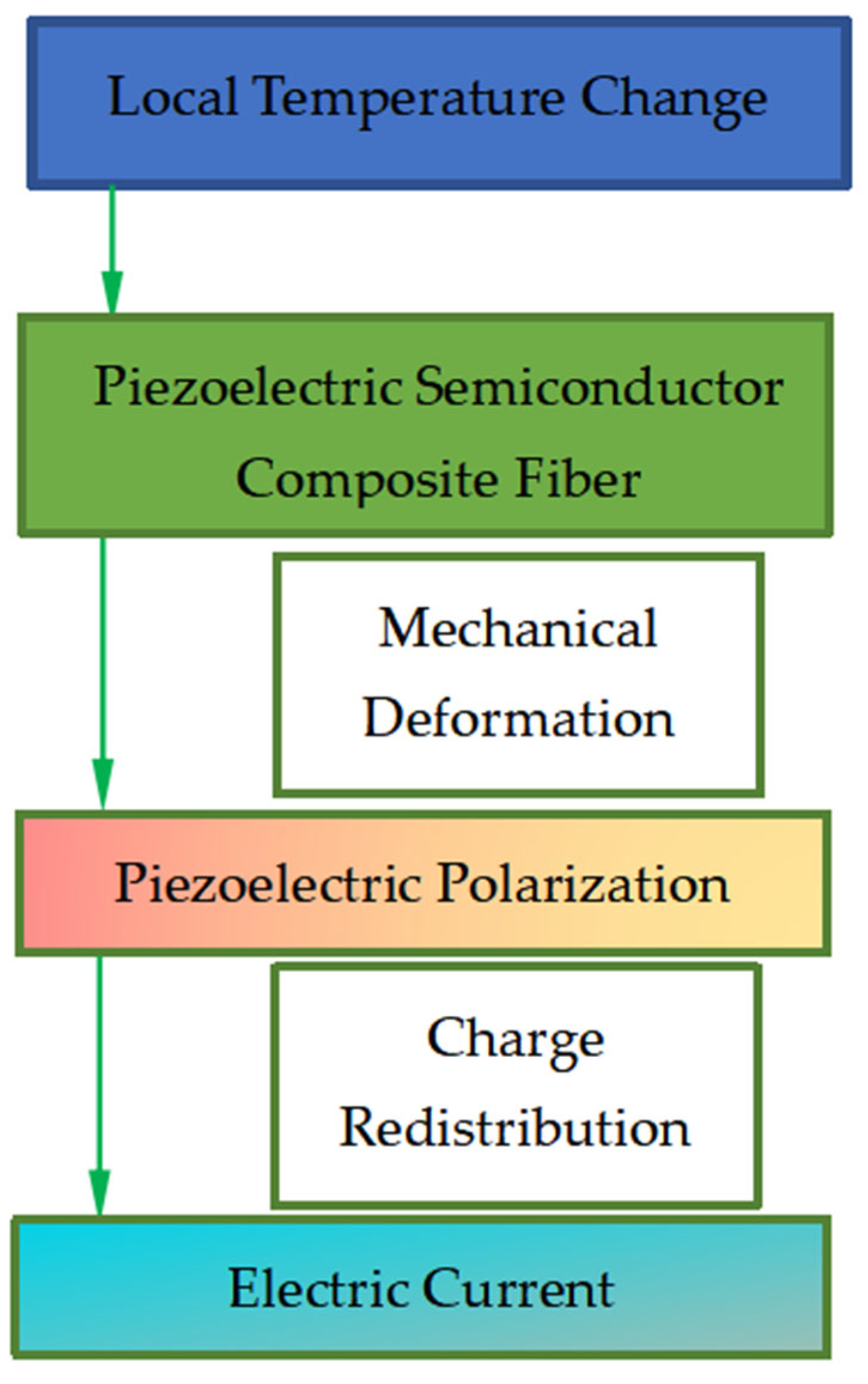
Figure 1. Working mechanism.
Crystals 14 00628 g001
Figure 2. A composite fiber under a local temperature change.
Crystals 14 00628 g002
Figure 3. Fields in composite fiber under different temperature changes. (a) Electric potential φ; (b) electric field E3; (c) polarization intensity P3; (d) electric displacement D3; (e) effective polarization charge density ρP; (f) electron concentration perturbation Δn; (g) total charge density ρPqΔn; and (h) electron current density J 3 n . (n0 = 1 × 10²¹ m−3).
Crystals 14 00628 g003aCrystals 14 00628 g003b
Figure 4. Fields in composite fiber at different n0. (a) φ; (b) E3; (c) P3; (d) D3; (e) ρP; (f) Δn; and (g) ρPqΔn. (θ = 1 K).
Crystals 14 00628 g004aCrystals 14 00628 g004b
Figure 5. Variation in the field of the composite fiber with n0 at different temperature changes. (a) Electric displacement D3 (x3 = 0 μm) and (b) effective polarization charge density ρP (x3 = −1 μm).
Crystals 14 00628 g005
Figure 6. Fields in composite fiber at different h/c. (a) φ; (b) E3; (c) P3; (d) D3; (e) ρP; (f) Δn; and (g) ρPqΔn. (θ = 1 K and n0 = 1 × 10²¹ m−3).
Crystals 14 00628 g006aCrystals 14 00628 g006b
Disclaimer/Publisher’s Note: The statements, opinions and data contained in all publications are solely those of the individual author(s) and contributor(s) and not of MDPI and/or the editor(s). MDPI and/or the editor(s) disclaim responsibility for any injury to people or property resulting from any ideas, methods, instructions or products referred to in the content.