Article

The Thermal Stability and Photoluminescence of ZnSeO3 Nanocrystals Chemically Synthesized into SiO2/Si Track Templates

by
Gulnara Aralbayeva
1,
Gulnaz Sarsekhan
1,
Aiman Akylbekova
1,*,
Liudmila A. Vlasukova
2,
Zein Baimukhanov
1,*,
Vera Yuvchenko
3,
Assyl-Dastan Bazarbek
1,
Alma Dauletbekova
1,
Gaukhar Kabdrakhimova
1 and
Abdirash T. Akilbekov
1
1
Faculty of Physics and Technology, L.N. Gumilyov Eurasian National University, 2 Satbaev Str., Astana 010008, Kazakhstan
2
Faculty of Radiophysics and Computer Technologies, Belarusian State University, Kurchatov Street 5, 220045 Minsk, Belarus
3
A.N. Sevchenko Institute of Applied Physical Problems, Belarusian State University, Kurchatov Street 7, 220045 Minsk, Belarus
*
Authors to whom correspondence should be addressed.
Crystals 2024, 14(8), 730; https://doi.org/10.3390/cryst14080730
Submission received: 12 July 2024 / Revised: 8 August 2024 / Accepted: 15 August 2024 / Published: 17 August 2024
(This article belongs to the Section Inorganic Crystalline Materials)

Abstract

:
We report the effect of high-temperature treatment on the structure and photoluminescence of zinc selenite nanocrystals (ZnSeO3) deposited into SiO2/Si track templates. The templates were formed via irradiation with Xe ions (200 MeV, 108 ions/cm2) followed by etching in HF solution. ZnSeO3 nanocrystals were obtained via chemical deposition from the aqueous solution of ZnCl2 and SeO2 as Zn-, Se- and O-precursors. To estimate the thermal stability of the deposited precipitates, heat treatment was carried out at 800 and 1000 °C for 60 min in a vacuum environment. Scanning electron microscopy (SEM), X-ray diffractometry (XRD), photoluminescence (PL) spectroscopy, and electrical measurements were used for the characterization of ZnSeO3/SiO2nanoporous/Si nanocomposites. Thermal treatment of the synthesized nanocomposites resulted in structural transformations with the formation of ZnSe and ZnO phases while the content of the ZnSeO3 phase decreased. For the as-deposited and annealed precipitates, an emission in the range of (400 to 600) nm was observed. PL spectra were approximated by four Gaussian curves with maxima at ~550 nm (2.2 eV), 488 nm (2.54 eV), ~440 nm (2.82 eV), and 410 nm (3.03 eV). Annealing resulted in a decrease in PL intensity that was possibly due to the weight loss of the deposited substance during high-temperature treatment. The redistribution of maxima intensities after annealing was also observed with an increase in blue and violet emissions. The origin of the observed PL is discussed. The I–V curve analysis revealed an electronic type of conductivity for the ZnSeO3(NCs)/SiO2nanoporous/Si structure. The values of the specific conductivity were calculated within the percolation model. The sample annealed at 800 °C showed the highest specific conductivity of 8.5 × 10⁻⁶ Ohm−1·cm−1.

1. Introduction

Nanostructured materials (nanoparticles, nanowires, nanotubes, and others) exhibit unique size- and shape-dependent optical properties and thus find a wide range of applications in optoelectronic devices, photocatalysis, and solar energy conversion [1,2,3,4]. For optoelectronics, A2B6 compounds are of similar importance as silicon is for microelectronics. Nowadays, A2B6 nanostructures (ZnSe, ZnS, CdS, ZnO, and CdSe) are the focus of researchers’ attention because of their potential optoelectronic applications. Zinc oxide (ZnO) is among the most utilized n-type metal oxide semiconductor materials [5,6,7,8]. It has a direct band gap of 3.37 eV, high electron mobility, and a high exciton binding energy of 60 meV. Another material of interest is zinc selenide (ZnSe). It is a promising material in optoelectronic devices like LEDs (blue laser diodes), photodetectors, and photovoltaic devices because of its direct band gap (~2.7 eV) and significant exciton binding energy (21 meV) at room temperature. Various researchers have combined ZnO and ZnSe materials to create nanostructured zinc selenite (ZnSeO3) for photoanodes, photocatalysis, catalysts, and other possible applications [9,10]. One can suggest that zinc selenite may have additional beneficial properties compared to zinc oxide and selenide. However, there are still a lot of properties that are not known about ZnSeO3 and this is a disadvantage in possible applications. Different methods have been employed to synthesize nano-structured ZnSeO3, including: electrochemical deposition, which is considered more optimal for creating the desired crystal structure [11]; pulse laser deposition, used to create a buffer layer for solar cell structures [12]; hydrothermal techniques, which successfully prepared undoped and In-doped ZnSeO3 nanoparticles for photoanode applications [10]; and the co-precipitation method, where SeZnO3 nanosheets were explored as electrocatalysts in lithium–oxygen batteries (LOBs) [13].
A promising approach to the formation of a variety of nanostructured materials is their synthesis via deposition into nanoporous templates created using SiO2/Si wafers [14,15]. The creation of a-SiO2nanoporous/Si templates includes two steps. Firstly, the SiO2/Si wafer is irradiated with swift heavy ions, which results in the formation of latent tracks of damaged material in the silica layer [16,17]. Subsequent etching of latent tracks in selective etchants leads to the formation of track templates in a-SiO2/Si with controlled nanopore density, shape, and size from 10 nm to several micrometers. Various forms of one-dimensional Zn-based nanostructures have already been successfully synthesized using the template method in SiO2/Si track templates [18,19].
To improve the crystallinity and decrease the defect level of nanostructured semiconductors, their synthesis is generally carried out at elevated temperatures. An efficient tool to tune the properties of semiconductor nanomaterials is also post-synthesis annealing. Additionally, heat treatment provides the possibility to estimate the thermal stability of the created nanostructures. The effect of high-temperature treatment on ZnSeO3 nanostructures is under-researched, and there are only a few works in this field. For instance, the authors of [12] estimated the influence of deposition temperature in the range of (25 to 650 °C) on the structural and optoelectronic properties of Zn (O, Se) layers grown via pulsed laser vacuum deposition. They reported that polycrystalline and electrically conductive Zn (O, Se) layers were grown at the substrate temperatures of 500–650 °C. The layers grown at temperatures below 500 °C were amorphous and exhibited a semi-insulating behavior. In [20], the thermal stability of hydrates of ZnSeO3, their dehydration, and dissociation were investigated in a temperature range of (25–600 °C) under environmental conditions. It was shown that anhydrous ZnSeO3 presumably existed at a high temperature (up to 480 °C) and broke down within a temperature interval of 480–600 °C to form ZnO and SeO2.
The aim of this study is to estimate the thermal stability of ZnSeO3 nanocrystals (NCs) chemically deposited into a-SiO2nanoporous/Si templates as well as a transformation of its structure and optical and electrophysical properties during high-temperature treatment under vacuum conditions.

2. Materials and Methods
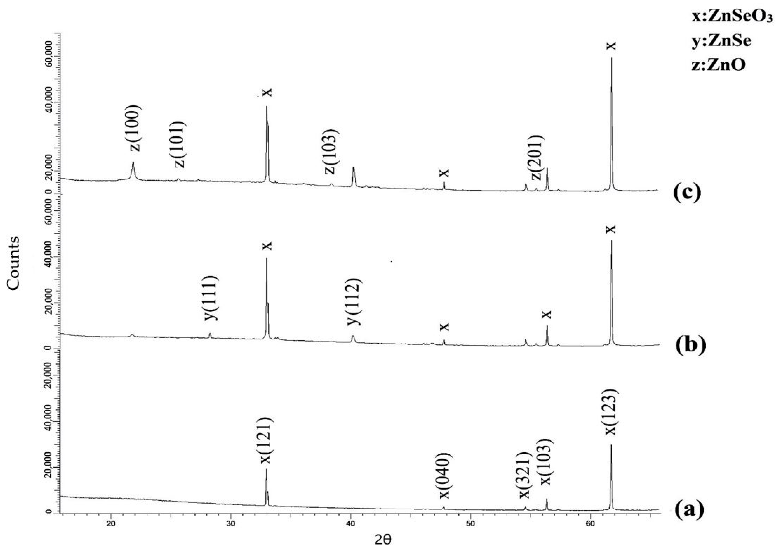
The a-SiO2/Si-n structure was fabricated through thermal oxidation of a silicon substrate in a wet oxygen atmosphere at 900 °C. The thickness of the oxide layer was 700 nm according to ellipsometry data. Afterward, samples with a size of 1 × 1 cm2 were cut from the oxidized Si wafer and irradiated with xenon ions with an energy of 200 MeV to a fluence of 108 ions/cm2 in the DC-60 accelerator (Astana, Kazakhstan), which in recent years has proven to be a powerful experimental facility for performing such experiments [21,22,23,24]. In order to form nanopores instead of latent tracks in the silica layers of the irradiated samples, chemical etching of SiO2/Si samples was carried out in a 4% aqueous solution of hydrofluoric acid (HF) with the addition of palladium chloride (PdCl2, m(Pd) = 0.025 g) at 18 ± 1 °C. Before track etching, ultrasonic cleaning of the surface of the samples in isopropanol for 15 min in a 6.SB25-12DTS ultrasonic cleaner (Xi’an Taikang Biotechnology Co., Ltd., Xi’an, China) was carried out. After treatment in HF, the samples were washed in deionized water (18.2 MOhm).
For ZnSeO3 deposition, solutions of zinc chloride (ZnCl2)—4 g/L and selenium dioxide (SeO2)—0.2 g/L in 100 mL of distilled water were prepared separately at room temperature and then mixed at pH = 3. Chemical deposition (CD) of precipitates in the track template samples was carried out under continuous stirring at a solution temperature of 18 °C. At 18 °C, the deposition process can be more precisely controlled, ensuring the stability of the solutions and minimizing unwanted side reactions. The duration of CD was varied from 5 to 60 min. Figure 1 depicts a brief scheme of the deposition process.
After CD, the samples with deposited precipitates were washed with distilled water. After washing, the samples were then dried in air at room temperature overnight.
Heat treatment of the samples with deposited precipitates was carried out in a vacuum at 800 and 1000 °C for 60 min using an AVERON furnace (Yekaterinburg, Russia). The heating rate was 30 °C/min.
The surface of the track templates was examined with a JSM 7500F scanning electron microscope (Tokyo Boeki, Tokyo, Japan). X-ray diffractometric analysis was performed on a D8 ADVANCE ECO X-ray (Karlsruhe, Germany) diffractometer using a Cu-anode X-ray tube in the angle range of 2θ 30–110° with a step of 0.01°. BrukerAXSDIFFRAC.EVAv.4.2 software and the international database ICDD PDF-2 were used for phase identification and crystal structure studies.
PL spectra were recorded in the range of 320 to 700 nm using a CM2203 spectrofluorometer (Solar, Minsk, Belarus) with Xe-lamp radiation at λ = 240 nm. Using two double monochromators ensured a minimum level of interference, guaranteeing high measurement accuracy. In all cases, we also subtracted the emission of the initial SiO2nanoporous/Si template from the resulting Pl spectra of templates with deposited precipitates.
An HP 66312A current source and 34401A Agilent multimeter (Keysight Technologies, Santa Rosa, CA, United States) were used to determine the electrical properties of the nanocrystals. The current–voltage characteristics (CVCs) were taken from an array of filled nanochannels, with an area of 0.3 cm2. A copper electrode with an area of 0.3 cm2 was deposited via thermal evaporation onto the surface of the sample with filled pores, and a second electrode was symmetrically formed on the backside. The CVCs were measured in constant voltage mode from −6 to 6 V in steps of 0.5 V. All CVCs were plotted using a second-order polynomial fit.

3. Results

The degree of pore filling as a function of deposition time was assessed on samples with an average pore diameter of 450 nm. As expected, the degree of pore filling increased with increasing CD time. Therefore, the filling degree increased from ~39% for the sample after CD for 15 min up to ~90% after CD for 30 min. Figure 2 illustrates the degree of pore filling after CD for 15 and 30 min. One can observe some not entirely filled pores as well as empty (not filled) ones on the surface of the sample after CD for 15 min. Conversely, completely filled pores as well as protrusion of the deposited substance from the nanopores were observed for the sample after CD for 30 min.
With a further increase in CD duration, the degree of pore filling remained practically unchanged. Thus, from the point of view of pore filling, the optimal deposition duration is 30 min. For further studies, precipitate deposition was carried out for 30 min at a solution temperature of 18 °C.
X-ray diffraction patterns taken from the samples with nanocrystals before and after annealing are shown in Figure 3. The identified X-ray peaks at 2θ = 33.00°, 47.76°, 54.53°, 56.41°, and 61.66° correspond to the orthorhombic phase of ZnSeO3. The most intensive peaks from ZnSeO3 are located at 2θ = 33.00° and 61.66° and belong to the (121) and (123) planes of the Miller indices of ZnSeO3, respectively. The intensities of these peaks increase significantly after heat treatment, indicating the densification and increase in the degree of crystallinity of the ZnSeO3 precipitates and the increase in the amount of polycrystalline phase compared to the amorphous one [12]. The relevant crystallographic parameters of nanoprecipitates in ion track templates of the as-deposited and annealed samples calculated from the XRD data are given in Table 1 and Table 2. The JCPDS-78-0446 pattern was taken to identify the X-ray peaks of orthorhombic ZnSeO3.
One can see from Table 2 that annealing leads to an increase in the ZnSeO3 crystallite size. Also, annealing results in the appearance of additional peaks in the XRD patterns, indicating the formation of new phases due to the thermal decomposition of ZnSeO3. For the sample annealed at 800 °C, peaks at 2θ = 28.0° and 40.2° appeared. These peaks correspond to ZnSe with a tetragonal structure. The appearance of peaks at 2θ = 21.9°, 25.8°, 38.3°, and 55.5° was observed for the sample annealed at 1000 °C. These peaks correspond to ZnO with a hexagonal structure. We can suppose that, firstly, heat treatment in a vacuum environment leads to oxygen component evaporation from the ZnSeO3 precipitates. As a result, the content of the ZnSeO3 phase decreases to 31.5% after annealing at 800 °C while the content of the tetragonal ZnSe phase amounts to 68.5%. With a further increase in temperature, selenium-based components start to evaporate [25], and, according to XRD data, after annealing at 1000 °C, precipitates are already mainly composed of the ZnO hexagonal phase (77.3%). The content of the ZnSeO3 orthorhombic phase amounts to 22.7% in the sample annealed at 1000 °C.

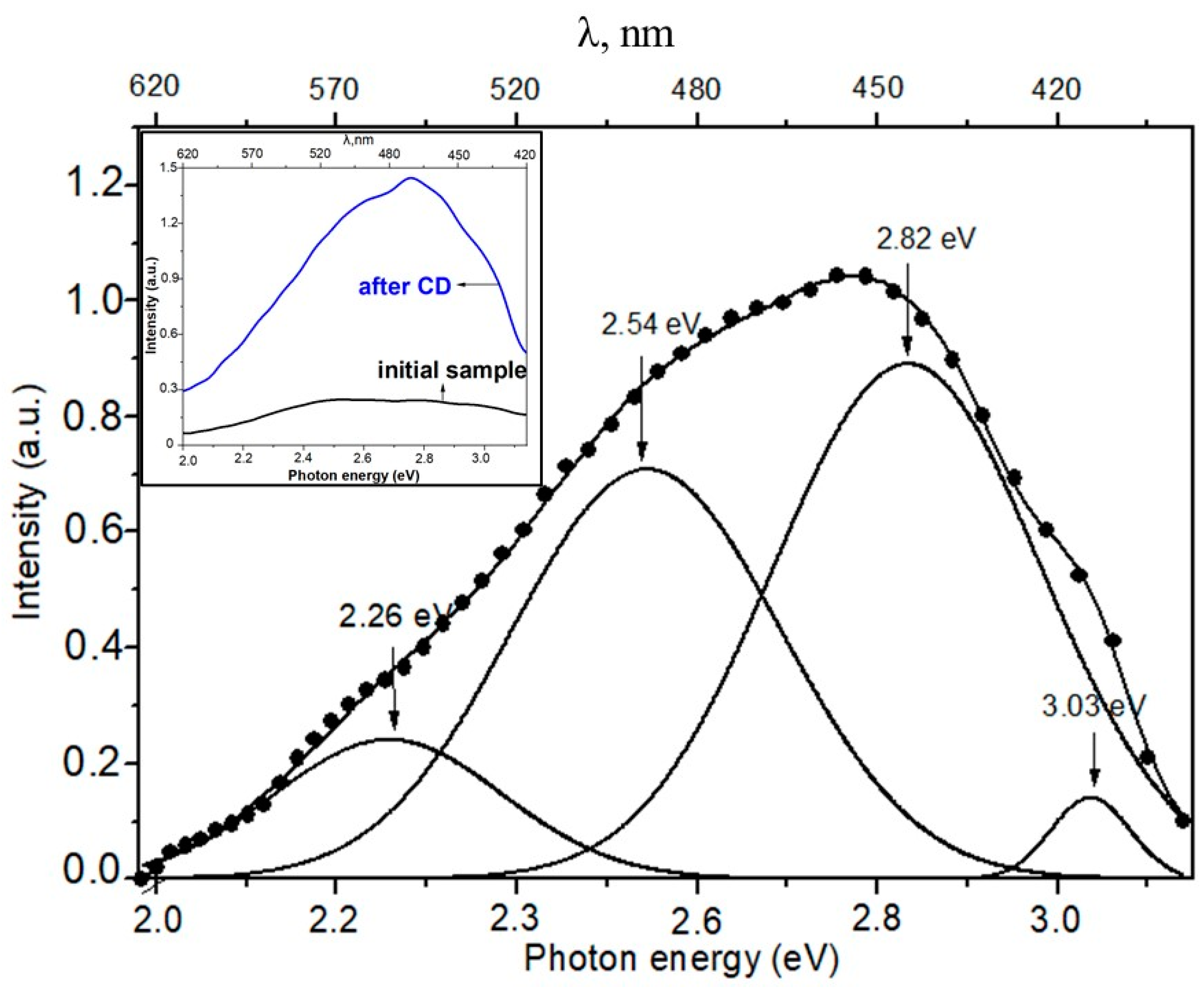
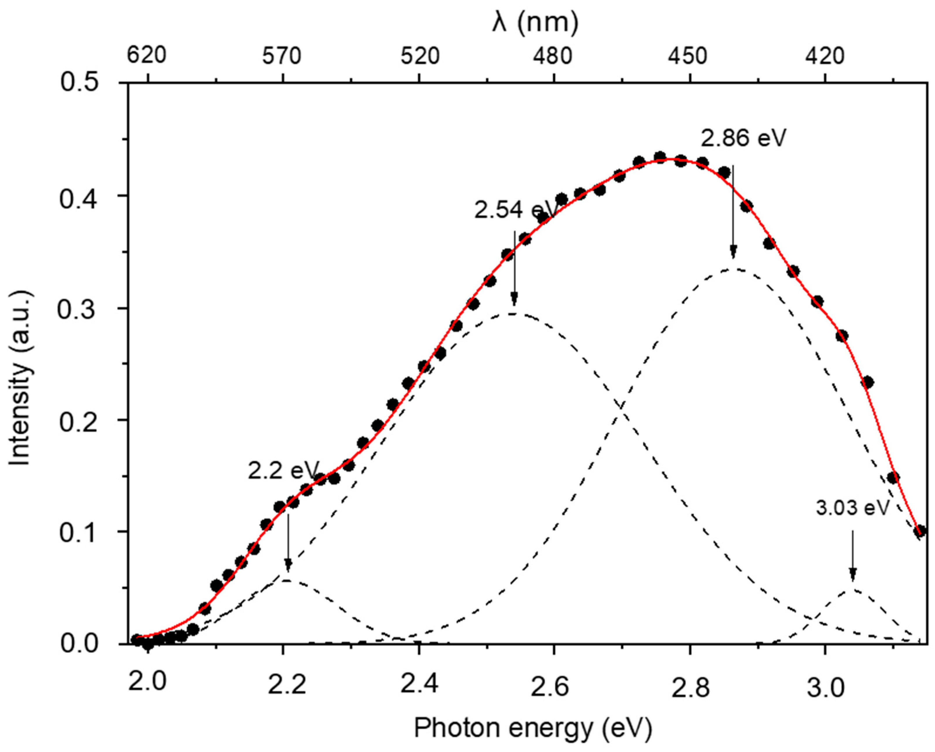
3.1. Photoluminescence

The PL spectrum of the sample with as-deposited NCs as well as the PL spectra of the annealed samples are shown in Figure 4, Figure 5 and Figure 6. For comparison, Figure 3 (inset) also shows the spectrum of the initial SiO2nanoporous/Si sample before nanocrystal deposition.
A wide band in the range of 400 to 600 nm dominates all spectra. It can be approximated by four Gaussian curves with maxima at ~550 nm (2.2 eV), 488 nm (2.54 eV), ~440 nm (2.82 eV), and 410 nm (3.03 eV). One can expect that the ZnSeO3 luminescence is a combination of luminescence from ZnSe and ZnO. According to [26] the green emission around 550 nm can be ascribed to deep-level trap emission originating from oxygen deficiency. The band at 488 nm is possibly due to some donor–acceptor pairs associated with Zn/Se vacancies and intermediate states [27]. The blue emission at around 440 nm, according to [28], can be ascribed to defects in ZnO caused by the presence of oxygen atoms in the interstices of the crystal lattice. The band at 410 nm can be attributed to the violet emission of ZnO nanoparticles and is probably due to the complex defects involving Zni and VZn and related to the interface traps at the ZnO grain boundaries [29].
Interestingly, the intensity of the as-deposited nanocrystals’ emission decreases after annealing while the emission maxima locations are practically the same for the as-synthesized and annealed precipitates. An explanation for the observed luminescence is given above based on its defect origin. One can suppose that a decrease in PL intensity after heat treatment confirms the defect origin of the emission and is related to the defect’s annealing. However, it is more realistic to suppose that this effect is mainly due to weight loss of the deposited substance during heat treatment. Estimation of the weight losses of the annealed samples was beyond the scope of our investigation. However, the weight losses can amount to nearly 30–40% for ZnSeO3 or ZnSe after high-temperature treatment [10,30].
One can observe the redistribution of intensity between the bands at 488, ~440 nm, and 410 nm in the annealed samples with the annealing temperature increase too. The intensity of blue and violet emissions at 440 and 410 nm increased for the sample annealed at 1000 °C in comparison with the sample annealed at 800 °C while the intensity of the band at 488 nm, conversely, decreased. As above, we attributed the band at 488 nm to some donor–acceptor pairs associated with Zn/Se vacancies and intermediate states, and the bands at 440 and 410 nm were ascribed to the radiative centers related to defects in the ZnO phase. An increase in the intensity of blue and violet emission from ZnO nanocrystals for the sample annealed at higher temperatures is in good agreement with the XRD data. According to the XRD data, after annealing at 1000 °C, the precipitates were mainly composed of the ZnO phase (77.3%) while the content of the ZnSeO3 phase decreased to 22.7%. For the sample annealed at 800 °C, the content of the ZnSeO3 and ZnSe phases amounted to 31.5 and 68.5%, respectively. The emission at 488 nm is related to ZnSe, and it is reasonable to suppose that it should be more intensive from the sample with the higher content of the ZnSe phase.

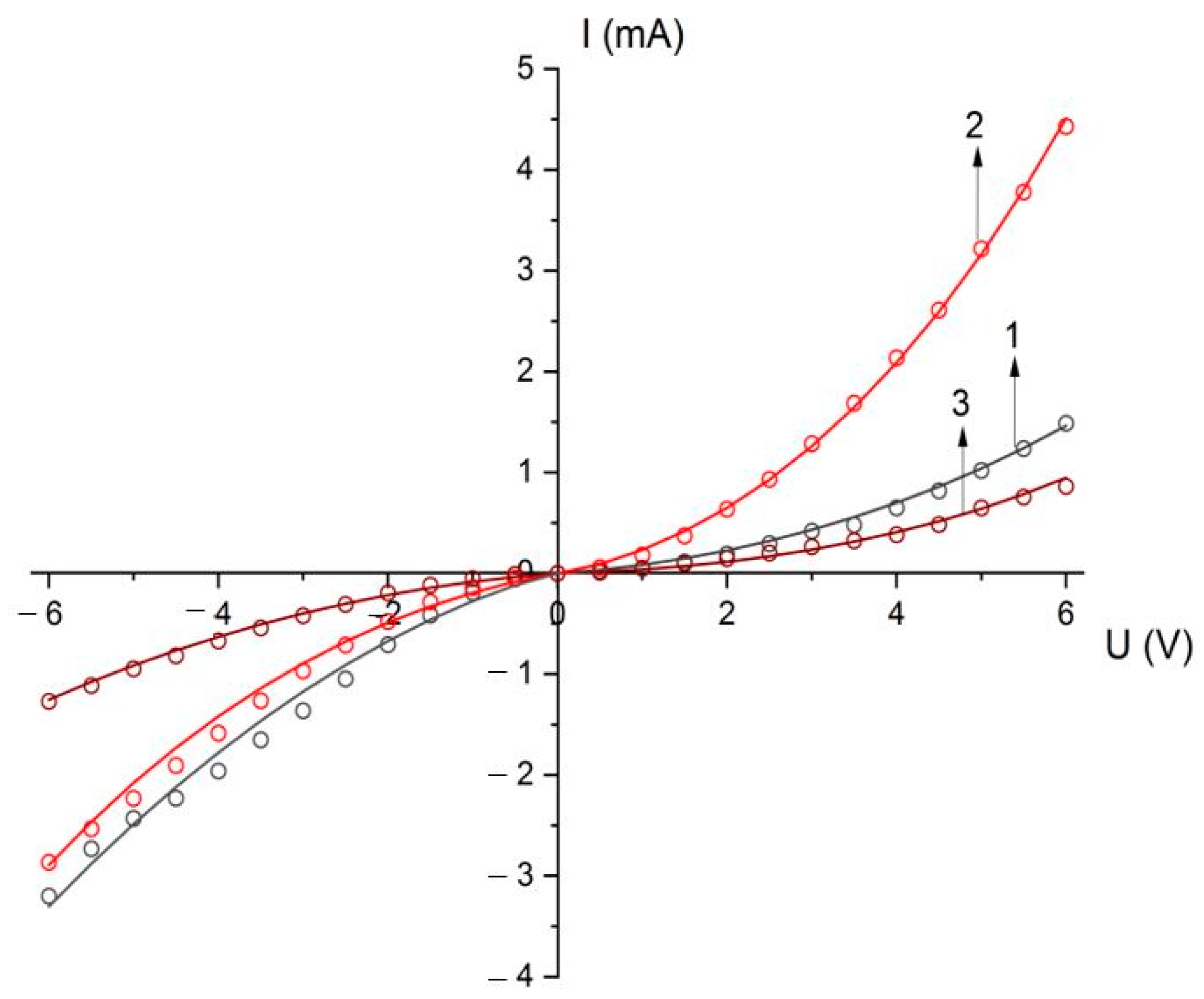
3.2. Electrical Properties

To investigate the electrical properties of ZnSeO3 nanocrystals obtained via chemical deposition, their current–voltage characteristics (I–V curves) were studied. The setup scheme for the current–voltage measurement was as follows: a sample with deposited nanocrystals was placed between two metal plates that overlapped only a part of the sample with nanochannels. The size of this part was 0.3 cm2. The plates were then connected to a current source by the series connection of a multimeter.
Figure 7 shows the current–voltage characteristics for the sample with the as-deposited NCs and for the annealed samples.
The initial Si substrate for the growth of the SiO2 film had n-type conductivity. From the I–V curve analysis, it can be concluded that the structure ZnSeO3(NCs)/SiO2nanoporous/Si shows an electronic type of conductivity. The current–voltage curves of the structures are essentially nonlinear. The specific conductance of the entire structure with pores filled with nanocrystals can be calculated using the following formula:
σ = d I d U l A
where l is the length of nanocrystal arrays (corresponding approximately to the thickness of the oxide layer—700 nm); A is the contact area; and d I d U is the differential conductance, calculated for high forward voltage from the I–V characteristic.
The conductivity of each conical wire consisting of a nanocrystal array can be calculated using:
σ W = d I d U l A Φ η π r 2
where Φ is the pore density (assumed to be equal to ion fluence—each ion creates an etchable track); η is part of the completely filled pores; and r is the radius of a cylindrical nanopore (considering the cone-shaped nanopores, the average radius value was taken equal to 112.5 nm according to the SEM images).
The nonlinear behavior of the I–V curves can be interpreted using the percolation conductivity model for polycrystalline semiconductors [31,32,33]. In fine-grained material, barrier disorder, caused by random crystallographic orientation of the grains and by the variations in their sizes and composition, leads to the formation of a percolation structure in the material as it is divided into regions permitted or prohibited to the current carriers. The effective electrical conductivity of a polycrystal is controlled by the height of the critical barriers ξc, determining the percolation level of the random energy relief at the bottom of the conductivity band. Current carriers pass only through barriers included in the critical subnet (infinite cluster), which contains only the barriers with heights ξξc. The height distribution function of the inter-grain barriers f(ξ) controls the percolation level ξc, which is determined by the equation [31]
p c = ξ min ξ c f ( ξ ) d ξ
where pc is a correlation threshold. In strong electric fields, a change in the electrical conductivity of the barrier-disordered system appears not only due to barrier lowering by the applied field E but also due to the rearrangement of the critical subnet responsible for current transport. In this case, the expression for I–V curves could be written as [31]:
I = I 0 exp c e E ¯ L k b T f ν ( ξ c ) 1 / ( 1 + ν )
where c is a constant factor: c ≈ 1; e is the electron charge; L is the average grain size; kb is the Boltzmann constant; Ē is the electric field strength; and ν ≈ 0.9 ÷ 1 in the three-dimensional case [34].
Conductivity in disordered polycrystalline semiconductors in the case of grain boundary states filling under applied voltage could be expressed as [20]:
σ = σ 0 exp c V 0 / k b T e E ¯ L δ V 1 / ν
where V0 is the amplitude of random variations in the barrier height for different grain boundaries and δV is the increase in the barrier height due to the capture of electrons.
Conductivity is calculated in the assumption that grain-boundary states are already occupied.
σ = σ 0 exp D E ¯ 1 / ( 1 + ν )
is in good agreement with data on the electrical conductivity of ZnO-based varistors in which grain-boundary states are already filled at low electric fields according to [32]. As stated in [35], repeated verification showed that inter-crystalline boundaries in A2B6 semiconductors act as acceptors. They accumulate negative charge at the surface states and thus create inter-crystalline barriers.
The experimental current–voltage curves are in good agreement with a scenario predicted by Formula (6). In more detail, current density could be described by the Pool-Frenkel-type equation [33] (ν = 1):
j = σ 0 E ¯ exp c e L Δ E ¯ k b T
where c has been taken equal to 1; L is equal to THE crystalline size from Table 2 for the main nanoprecipitate’s fraction for each sample; Δ is the value of the random potential; and σ0 is the ohmic conductivity in the low field. The fitted values of σ0 for all samples are given in Table 3. The best fit of our measured I–V curves was obtained with the value of Δ = 0.012 eV for the forward branch of I–V characteristics for all samples. This may indicate that although a partial decomposition of initial ZnSeO3 nanocrystals takes place during heat treatment with the formation of ZnSe and ZnO phases, the conductivity character does not undergo qualitative changes and is determined by the conductivity of the material of the phase with the largest content.
Thus, the highest value of the specific conductivity was observed for the sample annealed at 800 °C.

4. Conclusions

Zinc selenite nanocrystals were synthesized in a SiO2/Si track template via chemical deposition from an aqueous solution of ZnCl2 and SeO2 as Zn-, Se-, and O-precursors at 18 °C. The track template was formed via irradiation with 200 MeV Xe ions up to a fluence of 108 ions/cm2 followed by chemical etching of latent tracks in the aqueous solution of hydrofluoric acid.
Analysis of XRD diffractograms from the as-deposited precipitates revealed a formation of ZnSeO3 nanocrystals with an orthorhombic structure. Thermal treatment of the synthesized nanocomposites at 800 °C in a vacuum resulted in the formation of ZnSe nanocrystals with a tetragonal structure due to the evaporation of oxygen components from the ZnSeO3 precipitates. The resulting content of the ZnSeO3 phase decreased to 31.5% while the content of the ZnSe phase amounted to 68.5%. With a further increase in temperature, selenium-based components started to evaporate, and, according to XRD data, after annealing at 1000 °C, the precipitates were already composed mainly of the hexagonal phase of ZnO (77.3%) and the orthorhombic phase of ZnSeO3 (22.7%). Annealing also led to an increase in the ZnSeO3 crystallite size.
For the as-deposited and annealed precipitates, an emission in the range of 400 to 600 nm was observed. PL spectra were approximated by four Gaussian curves with maxima at ~550 nm (2.2 eV), 488 nm (2.54 eV), ~440 nm (2.82 eV), and 410 nm (3.03 eV). It is supposed that the green emission arises presumably due to donor–acceptor pairs associated with Zn/Se vacancies and intermediate states as well as the violet emission being ascribed to the oxygen atoms in the interstices of the ZnO crystal lattice as well as the complex defects involving Zni and VZn and related to the interface traps at the ZnO grain boundaries. Annealing resulted in a decrease in PL intensity, which is possibly due to the weight loss of the deposited substance during high-temperature heat treatment. Annealing at 1000 °C led to a redistribution of PL maxima intensity with the increase in violet emission while the green emission decreased.
The I–V curves analysis revealed an electronic type of conductivity for the structure ZnSeO3(NCs)/SiO2nanoporous/Si. The values of the specific conductivity were calculated within the percolation model. The sample annealed at 800 °C showed the highest specific conductivity of 8.5 × 10⁻⁶ Ohm−1·cm−1.

Author Contributions

Conceptualization, A.A. and G.S.; methodology, A.D. and A.T.A.; software, L.A.V.; investigation, A.A., Z.B. and V.Y.; formal analysis, L.A.V.; resources, Z.B., G.A. and A.T.A.; data curation, G.K. and G.S.; writing—original draft preparation, A.A, G.A. and L.A.V.; funding, A.A.; writing—review and editing, A.A., Z.B., G.A. and A.-D.B. All authors have read and agreed to the published version of the manuscript.

Funding

This research was funded by Ministry of Science and Higher Education of the Republic of Kazakhstan, AP13268607.

Data Availability Statement

Data are contained within the article.

Acknowledgments

This article was prepared as part of the implementation of the scientific project of grant funding for young scientists under the “Zhas Galym” project for 2022–2024 of the Science Committee of the Ministry of Science and Higher Education of the Republic of Kazakhstan AP13268607 “Features of the formation of semiconductor nanostructures in a track template SiO2/Si”.

Conflicts of Interest

The authors declare no conflicts of interest.

References

  1. Machín, A.; Fontánez, K.; Arango, J.C.; Ortiz, D.; De León, J.; Pinilla, S.; Nicolosi, V.; Petrescu, F.I.; Morant, C.; Márquez, F. One-Dimensional (1D) Nanostructured Materials for Energy Applications. Materials 2021, 14, 2609. [Google Scholar] [CrossRef] [PubMed]
  2. Xu, C.; Anusuyadevi, P.R.; Aymonier, C.; Luque, R.; Marre, S. Nanostructured materials for photocatalysis. Chem. Soc. Rev. 2019, 48, 3868–3902. [Google Scholar] [CrossRef] [PubMed]
  3. Wang, W.; Qi, L. Light management with patterned micro-and nanostructure arrays for photocatalysis, photovoltaics, and optoelectronic and optical devices. Adv. Funct. Mater. 2019, 29, 1807275. [Google Scholar] [CrossRef]
  4. Wu, C.; Wang, K.; Batmunkh, M.; Bati, A.S.; Yang, D.; Jiang, Y.; Priya, S. Multifunctional nanostructured materials for next generation photovoltaics. Nano Energy 2020, 70, 104480. [Google Scholar] [CrossRef]
  5. Ghos, B.C.; Farhad, S.F.U.; Patwary, M.A.M.; Majumder, S.; Hossain, A.; Tanvir, N.I.; Rahman, M.; Tanaka, T.; Guo, Q. Influence of the Substrate, Process Conditions, and Postannealing Temperature on the Properties of ZnO Thin Films Grown by the Successive Ionic Layer Adsorption and Reaction Method. ACS Omega 2021, 6, 2665–2674. [Google Scholar] [CrossRef] [PubMed]
  6. Constantinoiu, I.; Viespe, C. ZnO metal oxide semiconductor in surface acoustic wave sensors: A review. Sensors 2020, 20, 5118. [Google Scholar] [CrossRef] [PubMed]
  7. Cui, J. Zinc oxide nanowires. Mater. Charact. 2012, 64, 43–52. [Google Scholar] [CrossRef]
  8. Rahman, F. Zinc oxide light-emitting diodes: A review. Opt. Eng. 2019, 58, 010901. [Google Scholar] [CrossRef]
  9. Hong, T.; Liu, Z.; Liu, H.; Liu, J.; Zhang, X.; Han, J.; Wang, B. Preparation and enhanced photoelectrochemical performance of selenite-sensitized zinc oxide core/shell composite structure. J. Mater. Chem. A 2015, 3, 4239–4247. [Google Scholar] [CrossRef]
  10. Maswanganye, M.W.; Kabongo, G.L.; Mathevula, L.E.; Mothudi, B.M.; Dhlamini, M.S. Unveiling the effect of strain engineering on the electrochemical properties of hydrothermally grown nanostructured indium doped ZnSeO3 for photoanode applications. Sci. Rep. 2023, 13, 20131. [Google Scholar] [CrossRef]
  11. Dauletbekova, A.; Akylbekova, A.; Sarsekhan, G.; Usseinov, A.; Baimukhanov, Z.; Kozlovskiy, A.; Vlasukova, L.A.; Komarov, F.F.; Popov, A.I.; Akilbekov, A.T. Ion-Track Template Synthesis and Characterization of ZnSeO3 Nanocrystals. Crystals 2022, 12, 817. [Google Scholar] [CrossRef]
  12. Polivtseva, S.; Spalatu, N.; Abdalla, A.; Volobujeva, O.; Hiie, J.; Bereznev, S. Pulsed laser deposition of Zn(O,Se) layers for optoelectronic application. Appl. Energy Mater. 2018, 1, 6505–6512. [Google Scholar] [CrossRef]
  13. Kim, Y.S.; Lee, G.H.; Sung, M.C.; Kim, D.W. Orthorhombically distorted perovskite SeZnO3 nanosheets as an electrocatalyst for lithium-oxygen batteries. Chem. Eng. J. 2021, 406, 126896. [Google Scholar] [CrossRef]
  14. Kaniukov, E.Y.; Ustarroz, J.; Yakimchuk, D.V.; Petrova, M.; Terryn, H.; Sivakov, V.; Petrov, A.V. Tunable nanoporous silicon oxide templates by swift heavy ion tracks technology. Nanotechnology 2016, 27, 115305. [Google Scholar] [CrossRef]
  15. Yakimchuk, D.; Bundyukova, V.; Smirnov, A.; Kaniukov, E. Express method of estimation of etched ion track parameters in silicon dioxide template. Phys. Status Solidi B 2019, 256, 1800316. [Google Scholar] [CrossRef]
  16. Benvagoub, A.; Toulemonde, M. Ion tracks in amorphous silica. J. Mater. Res. 2015, 30, 1529–1543. [Google Scholar] [CrossRef]
  17. Demyanov, S.E.; Kaniukov, E.Y.; Petrov, A.V.; Belonogov, E.K.; Streltsov, E.A.; Ivanov, D.K.; Sivakov, V. On the morphology of Si/SiO2/Ni nanostructures with swift heavy ion tracks in silicon oxide. J. Surf. Investig. X-Ray Synchrotron Neutron Tech. 2014, 8, 805–813. [Google Scholar] [CrossRef]
  18. Xie, Q.; Zhan, P.; Wang, W.; Li, Z.; Zhang, Z. Enhanced ultraviolet and visible photoluminescence of ZnO/Zn2SiO4/SiO2/Si multilayer structure. J. Alloys Compd. 2015, 642, 131–135. [Google Scholar] [CrossRef]
  19. Hsueh, T.J.; Chen, Y.W.; Chang, S.J.; Wang, S.F.; Hsu, C.L.; Lin, Y.R.; Chen, I.C. ZnO nanowire-based CO sensors prepared on patterned ZnO: Ga/SiO2/Si templates. Sens. Actuators B Chem. 2007, 125, 498–503. [Google Scholar] [CrossRef]
  20. Charykova, M.V.; Fokina, E.L.; Klimova, E.V.; Krivovichev, V.G.; Semenova, V.V. Thermodynamics of Arsenates, Selenites, and Sulfates in the Oxidation Zone of Sulfide Ores. IX. Physicochemical Formation Conditions and Thermal Stability of Zinc Selenites. Geol. Ore Depos. 2014, 56, 546–552. [Google Scholar] [CrossRef]
  21. Kozlovskiy, A.L.; Konuhova, M.; Shlimas, D.I.; Borgekov, D.B.; Zdorovets, M.V.; Shakirziyanov, R.I.; Garanin, Y.A.; Volodina, N.O.; Popov, A.I. Study of the Effect of Nanostructured Grains on the Radiation Resistance of Zirconium Dioxide Ceramics During Gas Swelling under High-dose Irradiation with Helium Ions. ES Mater. Manuf. 2024, 24, 1165. [Google Scholar] [CrossRef]
  22. Inerbaev, T.; Akilbekov, A.; Kenbayev, D.; Dauletbekova, A.; Shalaev, A.; Polisadova, E.; Konuhova, M.; Piskunov, S.; Popov, A.I. Color Centers in BaFBr Crystals: Experimental Study and Theoretical Modeling. Materials 2024, 17, 3340. [Google Scholar] [CrossRef]
  23. Kadyrzhanov, K.K.; Kozlovskiy, A.A.; Konuhova, M.; Popov, A.I.; Shlimas, D.D.; Borgekov, D.B. Determination of gamma radiation shielding efficiency by radiation-resistant composite ZrO2–Al2O3–TiO2–WO3–Nb2O5 ceramics. Opt. Mater. 2024, 154, 115752. [Google Scholar] [CrossRef]
  24. Kozlovskiy, A.L.; Shlimas, D.I.; Zdorovets, M.V.; Elsts, E.; Konuhova, M.; Popov, A.I. Investigation of the Effect of PbO Doping on Telluride Glass Ceramics as a Potential Material for Gamma Radiation Shielding. Materials 2023, 16, 2366. [Google Scholar] [CrossRef]
  25. Ou, K.; Wang, S.; Huang, M.; Zhang, Y.; Wang, Y.; Duan, X.; Yi, L. Influence of thickness and annealing on photoluminescence of nanostructured ZnSe/ZnS multilayer thin films prepared by electron beam evaporation. J. Lumin. 2019, 199, 34–38. [Google Scholar] [CrossRef]
  26. Ramya, E.; Rao, M.V.; Jyothi, L.; Rao, D.N. Photoluminescence and nonlinear optical properties of transition metal (Ag, Ni, Mn) doped ZnO nanoparticles. J. Nanosci. Nanotechnol. 2018, 18, 7072–7077. [Google Scholar] [CrossRef]
  27. Kazmersky, L.L. Polycrystalline and Amorphous Thin Films and Devices, 1st ed.; Academic Press: New York, NY, USA, 1980; pp. 135–152. [Google Scholar]
  28. Gao, F.; Naik, S.P.; Sasaki, Y.; Okubo, T. Preparation and opt ical property of nanosized ZnO electrochemically deposited in mesoporous silica films. Thin Solid Films 2006, 495, 68–72. [Google Scholar] [CrossRef]
  29. Ravindra, C.A. X-ray Diffraction and Photoluminescence Studies on ZnO Nanoparticles Synthesized by Sol Gel Auto Combustion Method Glycine Assisted Chelating Agent. J. Emerg. Technol. Innov. Res. 2021, 8, 143–147. [Google Scholar]
  30. Zuala, L.; Agarwal, P. Growth and characterization of ZnSe nanocrystals synthesized using solvothermal process. J. Mater. Sci. Mater. Electron. 2020, 31, 14756–14766. [Google Scholar] [CrossRef]
  31. Sukharev, V.Y. Percolation model of adsorption-induced response of the electrical characteristics of polycrystalline semiconductor adsorbents. J. Chem. Soc. Faraday Trans. 1993, 89, 559–572. [Google Scholar] [CrossRef]
  32. Glot, A.B. A model of non-Ohmic conduction in ZnO varistors. J. Mater. Sci. Mater. Electron. 2006, 17, 755–765. [Google Scholar] [CrossRef]
  33. Belyaev, A.P.; Rubets, V.P.; Antipov, V.V.; Grishin, V.V. Electrical and galvanomagnetic properties of cadmium telluride films synthesized under highly nonequilibrium conditions. Semiconductors 2008, 42, 1282–1285. [Google Scholar] [CrossRef]
  34. Shklovskii, B.I.; Efros, A.L. Electronic Properties of Doped Semiconductors; Springer: Berlin/Heidelberg, Germany, 1984; p. 388. [Google Scholar] [CrossRef]
  35. Belyaev, A.P.; Rubets, V.P.; Nuzhdin, M.Y. Electrical properties of cadmium telluride films synthesized in a thermal field with a temperature gradient. Semiconductors 2003, 37, 646–648. [Google Scholar] [CrossRef]
Figure 1. Scheme of synthesis for ZnSeO3 nanoprecipitates’ chemical deposition into SiO2 nanoporous/Si templates.
Crystals 14 00730 g001
Figure 2. SEM images of the sample’s surface after chemical deposition for (a) 15 and (b) 30 min at 18 °C.
Crystals 14 00730 g002
Figure 3. XRD patterns of the deposited nanocrystals: (a)—before annealing, (b)—after annealing at 800 °C, and (c)—after annealing at 1000 °C for 60 min.
Crystals 14 00730 g003
Figure 4. PL spectrum of the as-deposited nanocrystals: inset—spectra of the template with filled pores and the initial template before deposition.
Crystals 14 00730 g004
Figure 5. PL spectrum of the nanocrystals after annealing at 800 °C.
Crystals 14 00730 g005
Figure 6. PL spectrum of the nanocrystals after annealing at 1000 °C.
Crystals 14 00730 g006
Figure 7. I–V curves for the samples with nanocrystals. Open circles—experimental data; lines—data fitting with (7). 1—the as-deposited sample at a deposition duration of 30 min. 2—the sample after annealing at 800 °C; and 3—the sample after annealing at 1000 °C.
Crystals 14 00730 g007
Table 1. Crystallographic parameters of the as-deposited nanocrystals.
PhaseStructure TypeSpace Grouphkl2θ°d, ÅCrystalline Size, nmCell Parameters, ÅPhase Content, %Volume, Å3
x: ZnSeO3OrthorhombicPnma (62)12133.002.7121.17a = 5.94 b = 7.61 c = 5.10100231.41
04047.761.90
32154.531.68
10356.411.63
12361.661.50
Table 2. Crystallographic parameters of the nanoprecipitates after annealing.
SamplePhaseSpace Group2θ°Lattice Parameter, ÅCrystalline Size, nmPhase Content, %Volume, Å3
After annealing at 800 °Cy: ZnSe (PDF-01-077-8903), TetragonalP4/nmm (129)28.0
40.2
a = 3.97 c = 5.2325.768.582.57
x: ZnSeO3
(JCPDS-78-0446)
Orthorhombic
Pnma (62)33.002
47.76
54.53
56.41
61.656
a = 5.94 b = 7.61 c = 5.1026.5231.5231.41
After annealing at 1000 °Cz: ZnO (PDF-01-070-8070), HexagonalP63mc (186)21.9
25.8
38.3
55.5
a = 3.27 c = 5.23 37.577.348.47
x: ZnSeO3
(JCPDS-78-0446)
Orthorhombic
Pnma (62)33.002
47.76
54.53
56.41
61.656
a = 5.94 b = 7.61 c = 5.1036.1722.7231.41
Table 3. Electrophysical characteristics of nanocrystals in the as-deposited and annealed samples.
ValueAs-Deposited SamplesAfter Annealing at
800 °C
After Annealing at 1000 °C
Specific conductivity of the structure containing the nanocrystal arrays,
σ, Ohm−1·cm−1
1.0 × 10−73.2 × 10−75.9 × 10⁻⁸
Specific conductivity of a conical wire consisting of nanocrystals
σW, Ohm−1·cm−1
2.7 × 10−68.5 × 10−61.5 × 10⁻⁶
Random potential Δ, eV0.0120.0120.012
Ohmic conductivity for low-field σ0, Ohm−1·cm−1 2.0 × 10−76.0 × 10−71.2 × 10⁻⁷
Disclaimer/Publisher’s Note: The statements, opinions and data contained in all publications are solely those of the individual author(s) and contributor(s) and not of MDPI and/or the editor(s). MDPI and/or the editor(s) disclaim responsibility for any injury to people or property resulting from any ideas, methods, instructions or products referred to in the content.

