

Electronic Properties of Atomic Layer Deposited HfO2 Thin Films on InGaAs Compared to HfO2/GaAs Semiconductors

Abstract
:1. Introduction
2. Materials and Methods
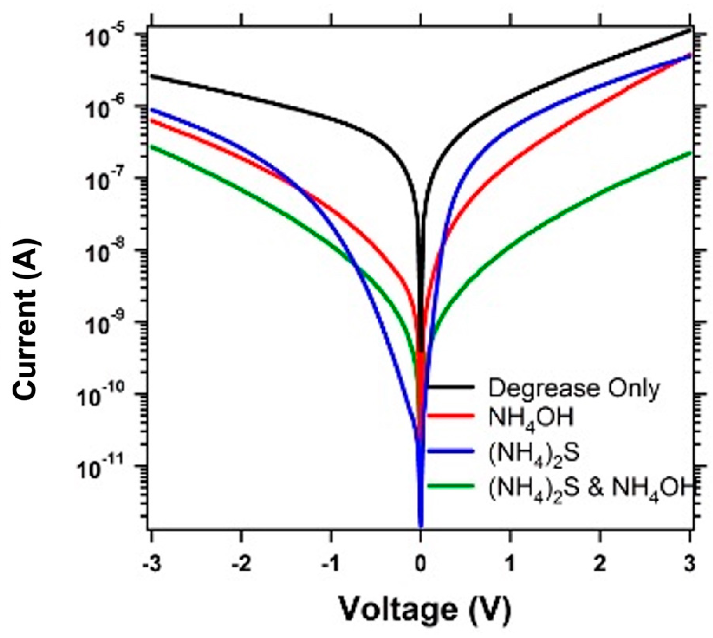
3. Results and Discussion
4. Conclusions
Author Contributions
Funding
Data Availability Statement
Acknowledgments
Conflicts of Interest
References
- Taur, Y. CMOS design near the limit of scaling. IBM J. Res. Dev. 2002, 43, 213–222. [Google Scholar] [CrossRef]
- Melitz, W.; Shen, J.; Kent, T.; Kummel, A.C.; Droopad, R. InGaAs surface preparation for atomic layer deposition by hydrogen cleaning and improvement with high temperature anneal. J. Appl. Phys. 2011, 110, 013713. [Google Scholar] [CrossRef]
- Suri, R.; Lichtenwalner, D.J.; Misra, V. Interfacial self cleaning during atomic layer deposition and annealing of HfO2 films on native (100)-GaAs substrates. Appl. Phys. Lett. 2010, 96, 112905. [Google Scholar] [CrossRef]
- Jia, Q.X.; McCleskey, T.M.; Burrell, A.K.; Lin, Y.; Collis, G.E.; Wang, H.; Li, A.D.; Foltyn, S.R. Polymer-assisted deposition of metal-oxide films. Nat. Mater. 2004, 3, 529. [Google Scholar] [CrossRef]
- Ritala, M. Atomic layer deposition of oxide thin films with metal alkoxides as oxygen sources. Science 2000, 288, 319–321. [Google Scholar] [CrossRef]
- Roy, K.; Mukhopadhyay, S.; Mahmoodi-Meimand, H. Leakage current mechanisms and leakage reduction techniques in deep-submicrometer CMOS circuits. Proc. IEEE 2003, 91, 305–327. [Google Scholar] [CrossRef]
- Assaderaghi, F.; Sinitsky, D.; Parke, S.; Bokor, J.; Ko, P.; Hu, C. Dynamic threshold-voltage MOSFET (DTMOS) for ultra-low voltage VLSI. IEEE Trans. Electron Devices 1997, 44, 414–422. [Google Scholar] [CrossRef]
- Laux, S.E. A Simulation Study of the Switching Times of 22- and 17-nm Gate-Length SOI nFETs on High Mobility Substrates and Si. IEEE Trans. Electron Devices 2007, 54, 2304–2320. [Google Scholar] [CrossRef]
- Ye, P.D.; Wilk, G.D.; Yang, B.; Kwo, J.; Gossmann, H.-J.L.; Hong, M.; Ng, K.K.; Bude, J. Depletion-mode InGaAs metal-oxide-semiconductor field-effect transistor with oxide gate dielectric grown by atomic-layer deposition. Appl. Phys. Lett. 2004, 84, 434. [Google Scholar] [CrossRef]
- Huang, M.L.; Chang, Y.C.; Chang, C.H.; Lee, Y.J.; Chang, P.; Kwo, J.; Wu, T.B.; Hong, M. Surface passivation of III-V compound semiconductors using atomic-layer-deposition-grown Al2O3. Appl. Phys. Lett. 2005, 87, 252104. [Google Scholar] [CrossRef]
- Huang, M.L.; Chang, Y.C.; Chang, C.H.; Lin, T.D.; Kwo, J.; Wu, T.B.; Hong, M. Comment on “Electric-field effect on carbon nanotubes in a twisted nematic liquid crystal cell”. Appl. Phys. Lett. 2006, 89, 012903. [Google Scholar] [CrossRef]
- Holt, D.B.; Yacobi, B.G. Extended Defects in Semiconductors; Cambridge University Press: Cambridge, UK, 2007; p. 482. [Google Scholar]
- Morita, M.; Ohmi, T.; Hasegawa, E.; Kawakami, M.; Ohwada, M. Growth of Native oxides on a silicon surface. J. Appl. Phys. 1990, 68, 1272–1281. [Google Scholar] [CrossRef]
- Lebedev, M.V.; Mankel, E.; Mayer, T.; Jaegermann, W. Etching of GaAs(100) with Aqueous Ammonia Solution: A Synchrotron-Photoemission Spectroscopy Study. J. Phys. Chem. C 2010, 114, 21385–21389. [Google Scholar] [CrossRef]
- Yuan, Z.L.; Ding, X.M.; Hu, H.T.; Li, Z.S.; Yang, J.S.; Miao, X.Y.; Chen, X.Y.; Cao, X.A.; Hou, X.Y.; Lu, E.D.; et al. Investigation of neutralized (NH4)2S solution passivation of GaAs (100) surfaces. Appl. Phys. Lett. 1997, 71, 3081–3083. [Google Scholar] [CrossRef]
- Morant, C.; Galan, L.; Sanz, J.M. An XPS study of the initial stages of oxidation of hafnium. Surf. Interface Anal. 1990, 16, 304–308. [Google Scholar] [CrossRef]
- Konda, R.B.; White, C.; Smak, J.; Mundle, R.; Bahoura, M.; Pradhan, A.K. High-k ZrO2 dielectric thin films on GaAs semiconductor with reduced regrowth of native oxides by atomic layer deposition. Chem. Phys. Lett. 2013, 583, 74–79. [Google Scholar] [CrossRef]
- White, C.; Donovan, T.; Cashwell, I.; Konda, R.B.; Sahu, D.R.; Xiao, B.; Bahoura, M.; Pradhan, A.K. Self-Cleaning and Electrical Characterizations of ZrO2 (HfO2)/GaAs (InGaAs) MOS Capacitor Fabricated by Atomic Layer Deposition. ECS Trans. 2013, 58, 325. [Google Scholar] [CrossRef]
- Chin, A.; Lin, B.; Chen, W.; Lin, Y.; Tsai, C. The Effect of Native Oxide on Thin Gate Oxide Integrity. IEEE Electron Device Lett. 1998, 19, 426–428. [Google Scholar] [CrossRef]
- Hamoud, G.A.; Kamaev, G.N.; Vergnat, M.; Volodin, V.A. Photocurrent in MIS structures based on germanosilicate films. St. Petersburg State Polytech. Univ. J. Phys. Math. 2024, 17, 149–154. [Google Scholar]
- Parratt, L.G. Surface studies of solids by total reflection of X-rays. Phys. Rev. B 1954, 95, 359–369. [Google Scholar] [CrossRef]
- Névot, L.; Croce, P. Caractérisation des surfaces par réflexion rasante de rayons X. Application à l’étude du polissage de quelques verres silicates. Rev. Phys. Appl. 1980, 15, 761. [Google Scholar] [CrossRef]
- Do, H.-B.; Luc, Q.-H.; Pham, P.V.; Phan-Gia, A.-V.; Nguyen, T.-S.; Le, H.-M.; De Souza, M.M. Metal-Induced Trap States: The Roles of Interface and Border Traps in HfO2/InGaAs. Micromachines 2023, 14, 1606. [Google Scholar] [CrossRef]
- Do, H.B.; Luc, Q.H.; Ha, M.T.H.; Huynh, S.H.; Nguyen, T.A.; Hu, C.; Lin, Y.C.; Chang, E.Y. Investigation of Mo/Ti/AlN/HfO2High-k Metal Gate Stack for Low Power Consumption InGaAs NMOS Device Application. IEEE Electron Device Lett. 2017, 38, 552–555. [Google Scholar] [CrossRef]
- Gougousi, T. Low-Temperature Dopant-Assisted Crystallization of HfO₂ Thin Films. Cryst. Growth Des. 2021, 21, 6411–6416. [Google Scholar] [CrossRef]
- Shandilya, S.; Madhu, C.; Kumar, V. Performance Analysis of the Gate All Around Nanowire FET with Group III–V Compound Channel Materials and High-k Gate Oxides. Trans. Electr. Electron. Mater. 2023, 24, 228–234. [Google Scholar] [CrossRef]


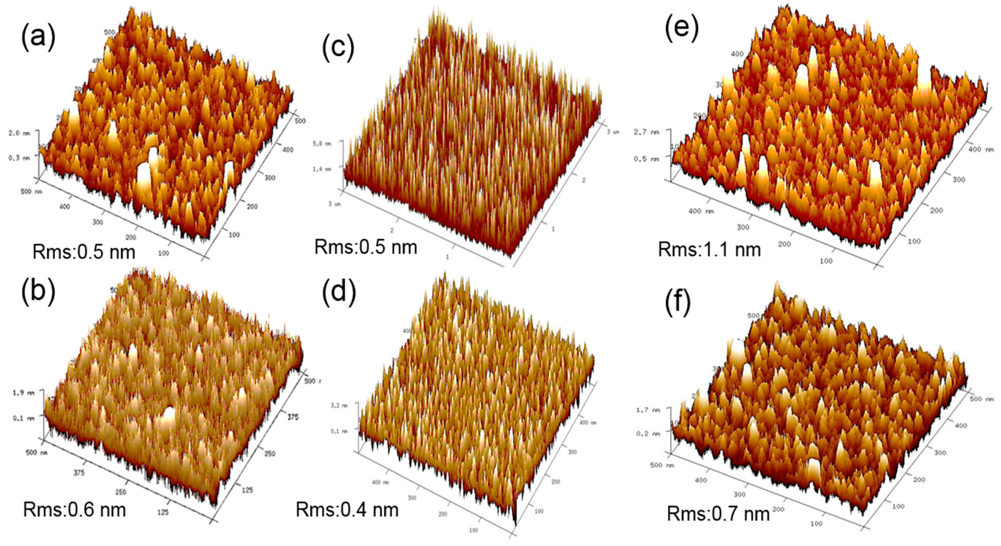
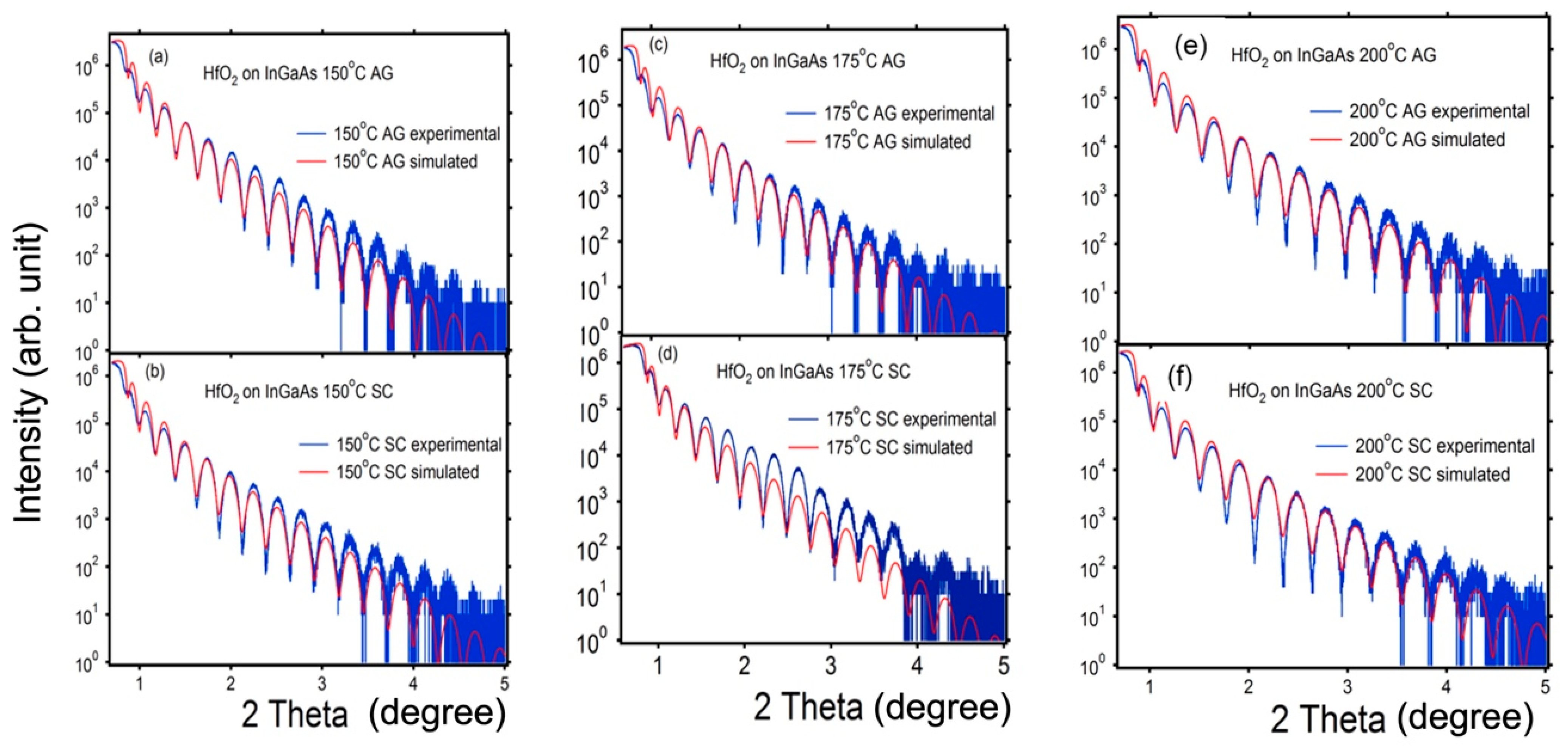
| Growth Temperature | Surface Treatment | HfO2 Film Thickness (nm) | HfO2 Film Density (g/cc) | HfO2 Surface Roughness (nm) | InGaAs/HfO2 Interface Roughness (nm) |
|---|---|---|---|---|---|
| 150 °C | As-grown | 31.35 | 9.11 | 0.74 | 0.70 |
| Self-cleaned | 31.6 | 9.08 | 0.67 | 0.64 | |
| 175 °C | As-grown | 30.17 | 9.16 | 0.73 | 0.68 |
| Self-cleaned | 30.1 | 9.01 | 0.71 | 0.72 | |
| 200 °C | As-grown | 27.9 | 9.03 | 0.66 | 0.63 |
| Self-cleaned | 28.16 | 9.05 | 0.61 | 0.58 |
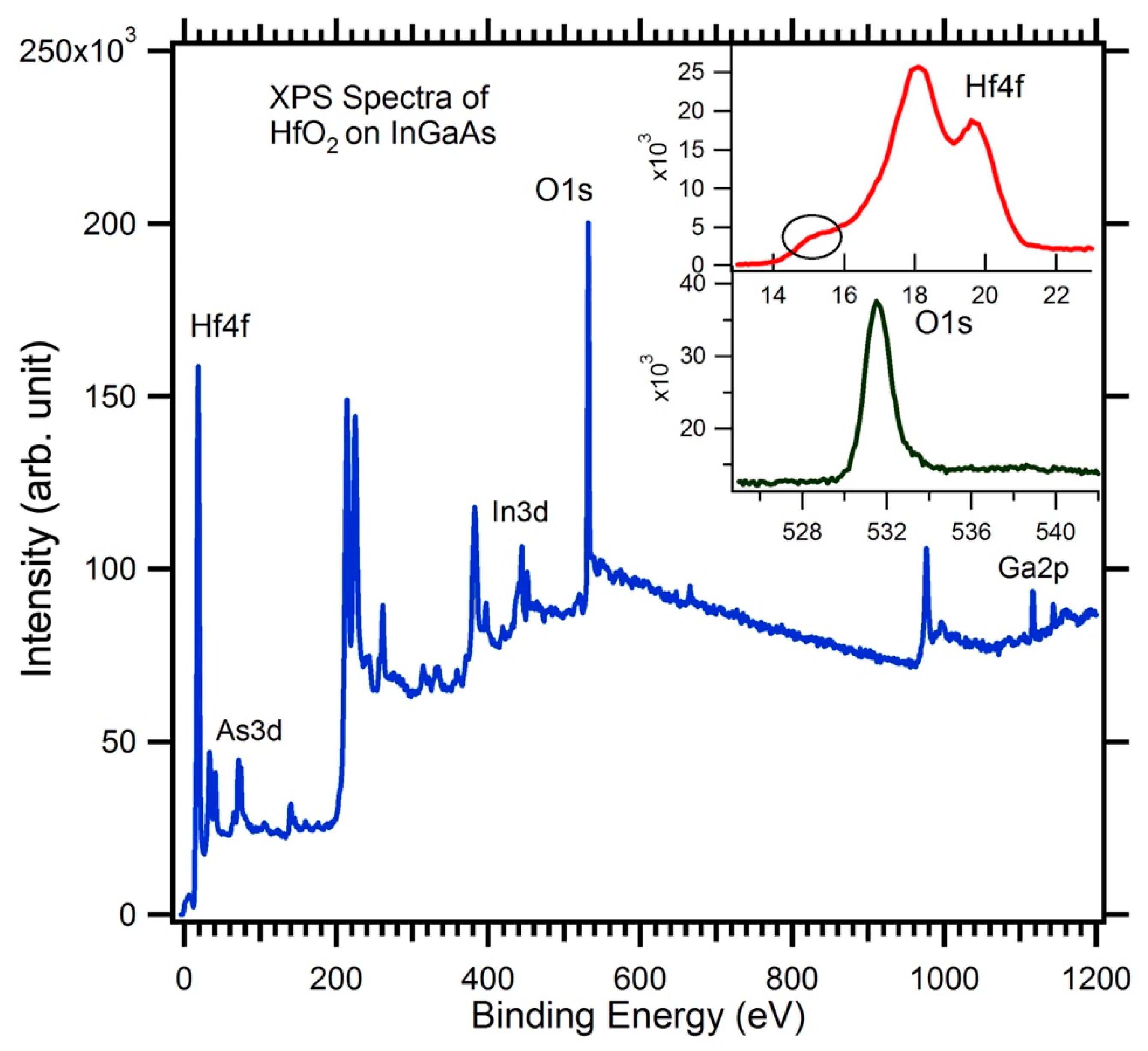
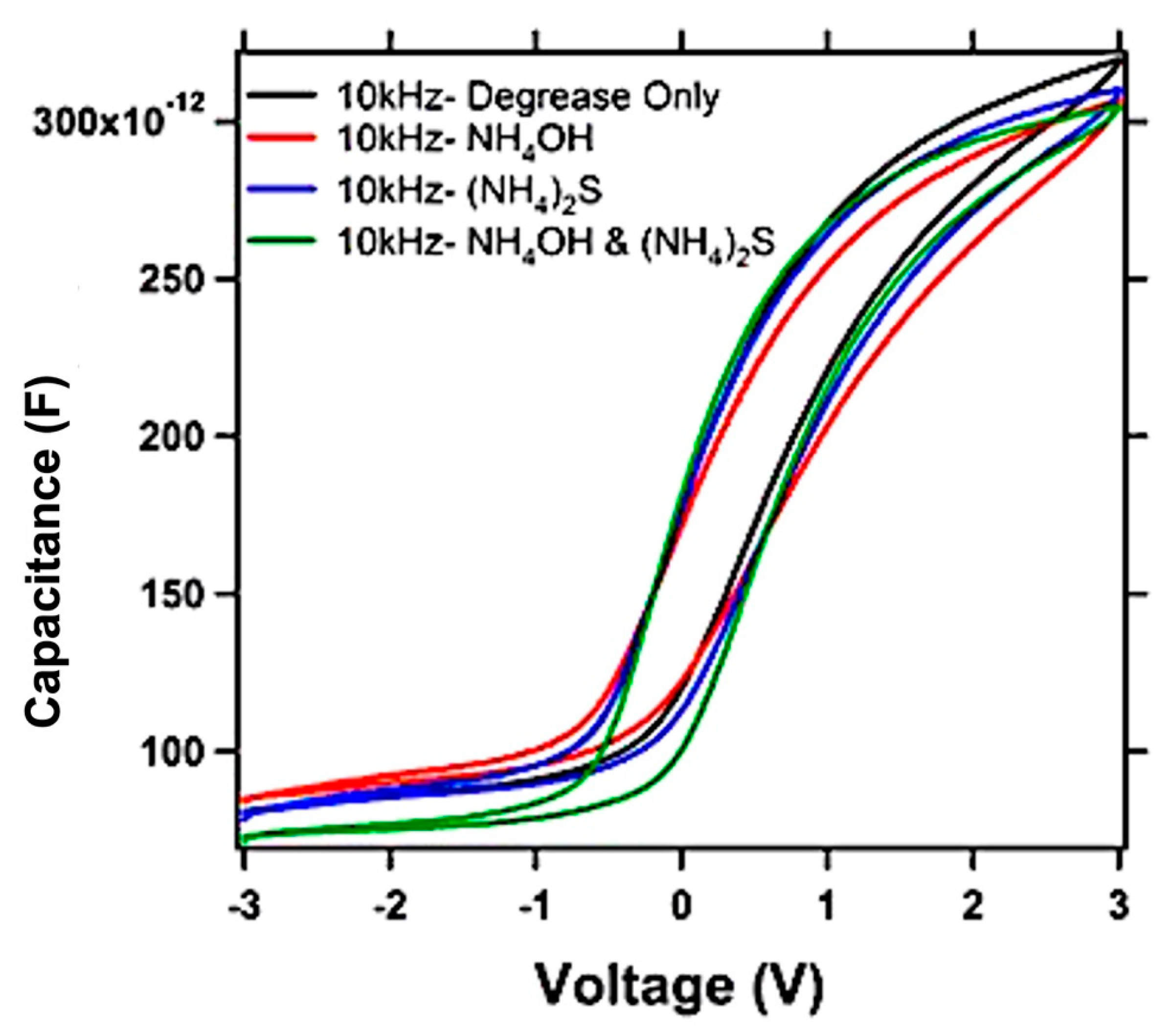
| Surface Pre-Treatment | HfO2 Film Thickness (nm) | HfO2 Film Density (g/cc) | HfO2 Surface Roughness (nm) |
|---|---|---|---|
| Degrease Only | 10.4 | 8.3 | 0.5 |
| NH4OH | 10.6 | 8.9 | 0.6 |
| (NH4)2S | 10.9 | 8.8 | 0.5 |
| NH4OH and (NH4)2S | 10.4 | 8.1 | 0.5 |
Disclaimer/Publisher’s Note: The statements, opinions and data contained in all publications are solely those of the individual author(s) and contributor(s) and not of MDPI and/or the editor(s). MDPI and/or the editor(s) disclaim responsibility for any injury to people or property resulting from any ideas, methods, instructions or products referred to in the content. |
© 2024 by the authors. Licensee MDPI, Basel, Switzerland. This article is an open access article distributed under the terms and conditions of the Creative Commons Attribution (CC BY) license (https://creativecommons.org/licenses/by/4.0/).
Share and Cite
Cashwell, I.K., Jr.; Thomas, D.A.; Skuza, J.R.; Pradhan, A.K. Electronic Properties of Atomic Layer Deposited HfO2 Thin Films on InGaAs Compared to HfO2/GaAs Semiconductors. Crystals 2024, 14, 753. https://doi.org/10.3390/cryst14090753
Cashwell IK Jr., Thomas DA, Skuza JR, Pradhan AK. Electronic Properties of Atomic Layer Deposited HfO2 Thin Films on InGaAs Compared to HfO2/GaAs Semiconductors. Crystals. 2024; 14(9):753. https://doi.org/10.3390/cryst14090753
Chicago/Turabian StyleCashwell, Irving K., Jr., Donovan A. Thomas, Jonathan R. Skuza, and Aswini K. Pradhan. 2024. "Electronic Properties of Atomic Layer Deposited HfO2 Thin Films on InGaAs Compared to HfO2/GaAs Semiconductors" Crystals 14, no. 9: 753. https://doi.org/10.3390/cryst14090753