Article

Fabrication of Microcrystalline Silicon Thin Film by Ionized Physical Vapor Deposition Process

1
Department of Energy Engineering, Assam Science and Technology University, Guwahati 781013, India
2
Department of Physics, Gauhati University, Guwahati 781014, India
3
Department of Physics, Sipajhar College, Darrang 784145, India
4
Institute of Advanced Study in Science and Technology, Guwahati 781035, India
5
Department of Physics, Pragjyotish College, Guwahati 781009, India
*
Author to whom correspondence should be addressed.
Crystals 2025, 15(2), 106; https://doi.org/10.3390/cryst15020106
Submission received: 21 June 2024 / Revised: 5 August 2024 / Accepted: 6 August 2024 / Published: 22 January 2025
(This article belongs to the Section Inorganic Crystalline Materials)

Abstract

:
The present manuscript describes the fabrication of microcrystalline silicon (µc-Si) thin films at room temperature using the ionized physical vapor deposition (iPVD) process. The iPVD chamber incorporates a planar DC magnetron and an additional RF coil to generate an intermediate dense plasma region between the target and the substrate. The intermediate dense plasma enhances the ionization of sputtered neutral Si atoms before deposition in the iPVD process. This process greatly impacts the structural, morphological, and optical characteristics of the Si thin films. X-ray diffraction (XRD) reveals that conventional PVD produces an amorphous Si thin film, while iPVD yields a µc-Si thin film with peaks at 28.5° and 47.3°, corresponding to the (111) and (220) planes of Si. Raman spectroscopy confirms the microcrystalline nature of the Si thin film, showing approximately 70% crystallinity in the iPVD process. FESEM images display a granular structure for PVD and a cauliflower-like structure for the iPVD process. AFM images indicate a significant reduction in surface roughness for iPVD films compared to the PVD process. UV-Visible absorption spectroscopy shows that the optical band gap (Eg) decreases from (1.7 ± 0.08) eV to (1.4 ± 0.05) eV while shifting from the PVD to iPVD process.

1. Introduction

Amorphous silicon (a-Si) and microcrystalline silicon (μc-Si) thin films have diverse applications. These include solar cells, field-effect transistors (FETs), thin-film transistors (TFTs), infrared sensing devices, and negative electrodes in lithium-ion (Li-ion) batteries [1,2,3]. Although a-Si dominates the solar cell industry, μc-Si thin films have garnered research interest due to their varied physical and optical properties. The μc-Si thin film is a dual-phase material, containing nano-sized crystallites or conglomerates of nano-crystallites and grain boundaries within the amorphous phase [4]. The crystallite size in the μc-Si thin film ranges from 20 to 700 nm [5]. μc-Si thin films exhibit properties between amorphous and polycrystalline Si, such as high carrier mobility, stability, and conductivity. The complex structure of μc-Si thin films results in intricate material properties, including an electronic structure, optical absorption, carrier transport, and stability. These enhanced properties significantly impact solar cell performance [6]. The use of μc-Si in the bottom cell of the MICROMORPH module has contributed to achieving stable conversion efficiency [7].
Due to the numerous advantages of plasma-based deposition processes, plasma-enhanced chemical vapor deposition (PECVD) is frequently employed for the deposition of Si thin films [8,9,10,11,12,13,14,15] compared to other chemical vapor deposition (CVD) methods. In the PECVD process, silane (SiH4) gas is utilized to prepare Si thin films. However, SiH4 is a highly flammable and toxic gas that requires many safety considerations as well as precautions for storage, transportation, and exhaust from the reactor [13,14,15]. In addition, a large volume of SiH4 gas is required as a raw material for the deposition of Si thin films in the PECVD technique. The majority of the gas is screened out by the vacuum system [15] in this technique. Additionally, CVD processes generally require high deposition temperatures, typically ranging from 200 °C to 800 °C [16,17]. For the fabrication of next-generation flexible electronic devices, Si thin films should be deposited on polymer substrates at low substrate temperatures [1]. Thus, it is very essential to identify some safe alternative techniques to deposit Si thin films at low (room) temperatures.
The physical vapor deposition (PVD) method represents a safe, cost-efficient, and eco-friendly alternative for preparing Si thin films [15]. DC magnetron sputtering, a widely utilized PVD technique, facilitates the deposition of metals, alloys, ceramics, and polymer thin films onto various substrates [18,19,20,21,22,23,24,25,26]. In DC magnetron sputtering, Si thin films are fabricated using a pure silicon target. This eliminates the need for hazardous precursor gases such as SiH4 and Si2H6, which are commonly employed in PECVD and other gas-phase dissociation techniques [27,28]. However, achieving crystallinity in Si thin films via DC magnetron sputtering necessitates high substrate temperatures and post-annealing at temperatures ranging from 450 °C to 950 °C [15,29]. A list of different approaches reported by researchers to fabricate μc-Si thin films using different techniques is presented in Table 1.
In most of the research works, microcrystalline hydrogenated Si thin films are developed at an elevated temperature by feeding hydrogen gas into the discharge. The very short effective diffusion length of the photo-generated carriers and the presence of the large number of dangling bonds, which trap the photo-generated carriers, are the major demerits of a-Si thin films developed using the magnetron sputtering technique [15].
In recent years, various ionized sputtering processes, collectively known as the ionized physical vapor deposition (iPVD) process, have been developed for thin film deposition [35,36,37,38,39,40]. The iPVD process involves generating an intermediate dense plasma between the target and substrate. This leads to the ionization of the sputtered atoms or molecules before deposition [35,36,37,38,39,40]. In the case of the PVD process, the neutral atoms or molecules of the target material are mainly deposited onto the substrate [41]. Recent studies [35,36] suggest that the iPVD process enhances thin film quality in terms of density and adhesion, even for geometrically complex substrates, due to the high degree of ionization of the sputtered materials. Several researchers have also reported on the impact of the reactive gas in the iPVD process, demonstrating its efficacy in depositing metallic coatings at reduced substrate temperatures [37,38]. As the degree of ionization of the sputtered atoms in the iPVD process increases, it becomes easier to control the energy and directionality of the target species reaching the substrate [42,43].
Despite these advancements, there remains a significant gap in research on the iPVD process for depositing pristine μc-Si thin films at room temperature. Thus, in the present work, pristine Si thin films are deposited on a glass substrate using the iPVD (i.e., RF plasma-assisted DC magnetron sputtering) process at room temperature without the addition of hydrogen gas into the discharge. For better understanding, a comparative study of thin film quality achieved through both PVD and iPVD processes is undertaken, focusing on the evolution of the microcrystallinity, uniformity, and optical band gap of the Si thin films.

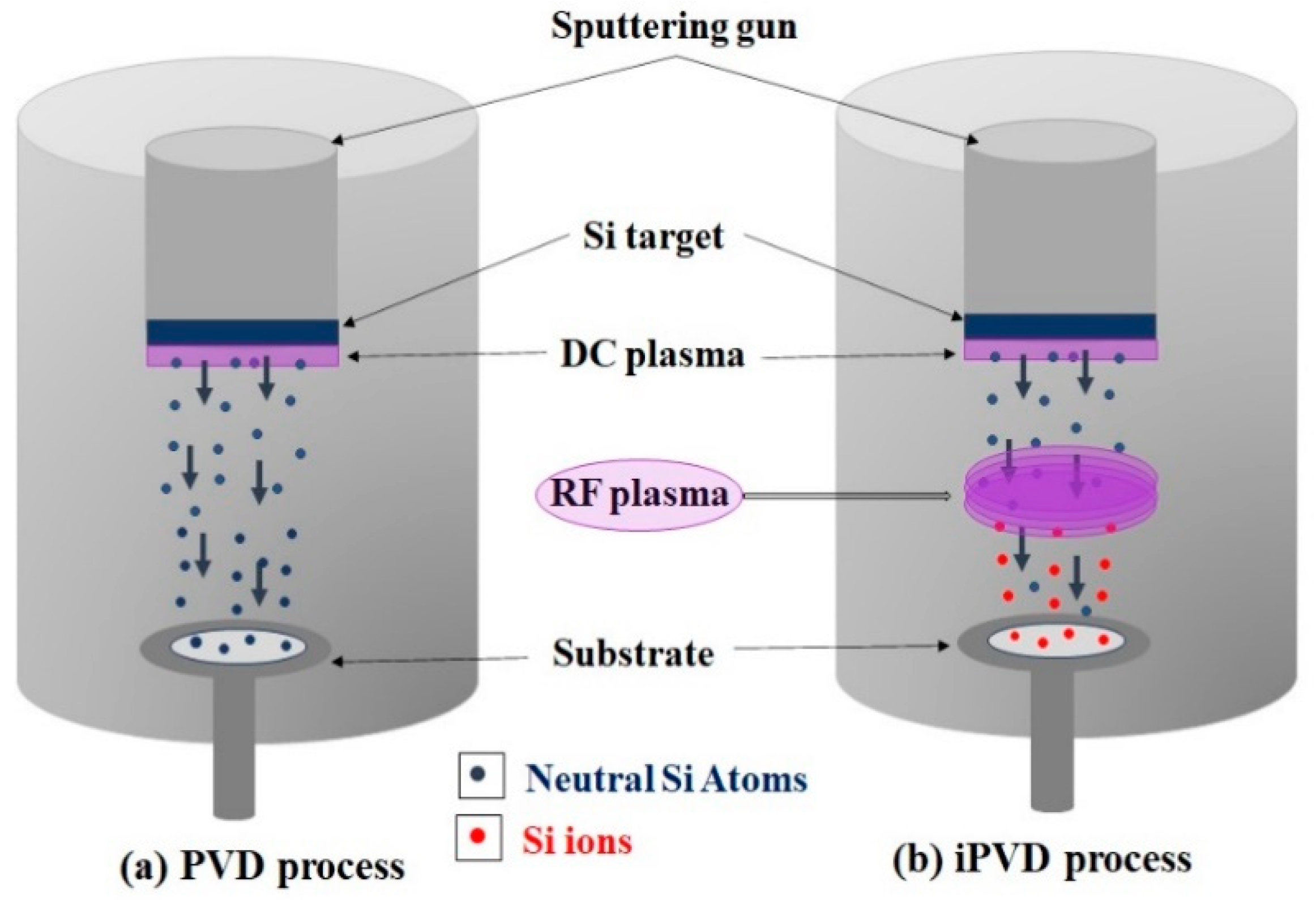
2. Experimental Set-Up

An ultra-high vacuum magnetron sputtering set-up, as shown in Figure 1, is used to deposit the Si thin film on a glass substrate at room temperature. The experimental chamber is made of SS304L material with a diameter of 400 mm and a height of 500 mm. The water circulation pipes are attached to the chamber wall for the circulation of cold water during the experiment. A planar DC magnetron is used in the present experimental assembly for sputtering the target atoms. A water-cooled Si target (diameter: 100.0 mm, thickness: 3.0 mm, and purity: 99.99%) is used for the deposition of Si thin films. The separation between the target and substrate is maintained at 100 mm. Prior to the experiment, the glass slides (substrate) are cleaned with acetone.
The experimental chamber is evacuated to a base pressure of ~10−7 mbar with the help of a turbo-molecular pump (TMP) (make: PFEIFFER, Asslar, Germany, model: D-35614) backed by a rotary pump (make: PFEIFFER, model: D-35614). An ionization gauge (make: PFEIFFER, model: PKR251) is used to measure the chamber pressure. A DC power supply (make: Aplab, Mumbai, India, 1000 V/2.5A) is used to sputter the Si atoms through magnetron sputtering in both the PVD and iPVD processes. Additionally, for the iPVD process, an RF power supply (make: RF VII Inc. Newfield, NJ, USA, max. power: 1.0 kW) is used to create an intermediate plasma between the target and the substrate to ionize the sputtered Si atoms. A copper coil with a diameter of 150 mm with two numbers of windings is used to launch the RF power to produce the intermediate plasma. The coil is placed midway between the target and the substrate, i.e., 50 mm below the target. To mitigate overheating of the copper coil and the target material, cold water is circulated continuously during the experiment. In the PVD process, the neutral sputtered atoms/molecules mainly contribute to the thin film growth. Due to the intermediate RF plasma produced between the target and the substrate, the iPVD process has a higher availability of ionized sputtered atoms, which helps to improve the quality of the thin film. A pictorial representation of the PVD and iPVD process is illustrated in Figure 2a,b.
Ultra-pure Argon (Ar) gas (purity: 99.999%) is used as the operating gas and is fed into the experimental chamber with the help of a digital flow controller (Alicat-MCM-100SCCM-D). The working pressure is maintained constant at 2.5 × 10⁻³ mbar for both experiments. The deposition time for both processes is carried out for 30 min. During the PVD process, there is no intermediate plasma between the target and the substrate. Thus, no RF power is launched to the copper coil. But, for the iPVD process, an RF power of 250 W is launched to the copper coil to produce an intermediate plasma. The detailed operational parameters for both the PVD and iPVD processes are given below in Table 2.
The crystal structure and surface morphology of the Si thin films are studied using XRD (Model: D8 Advanced, Bruker AXS, Karlsruhe, Germany), a Raman spectrometer (Horiba, LabRAM HR UV-VIS-NIR, Kyoto, Japan), FESEM (ZEISS Gemini, Sigma 300, Baden-Württemberg, Germany), and AFM (Model: NTEGRA Vita from NT-MDT, Limerick, Ireland). The crystallite size is calculated from XRD using Scherrer’s formula. The roughness of both Si thin films is estimated through AFM analysis. Optical emission spectroscopy (OES) is carried out to record the spectral line profiles during both processes. Furthermore, the optical property of the thin films is studied with the help of UV-visible spectroscopy.

3. Results and Discussion

Prior to the deposition of Si thin films, the plasma parameters are measured with the help of a cylindrical Langmuir probe (Tip length: 10 mm, Dia.: 0.25 mm) for both the PVD and iPVD processes. To avoid the deposition of Si on the probe tip, a glass tube with a diameter of 10 mm is fitted around the probe tip. To measure the plasma parameters, the Langmuir probe is placed 25 mm below the target to minimize the effect of the magnetic field on charge collection by the probe tip. From the I-V characteristics of the Langmuir probe, the plasma density is found to be (1.6 ± 0.07) × 1016/m3 and the electron temperature is found to be (1.48 ± 0.06) eV for the present operating conditions during the PVD process. In the iPVD process, the plasma density is observed as (6.72 ± 0.41) × 1016/m3 and the electron temperature is found to be (1.49 ± 0.09) eV.

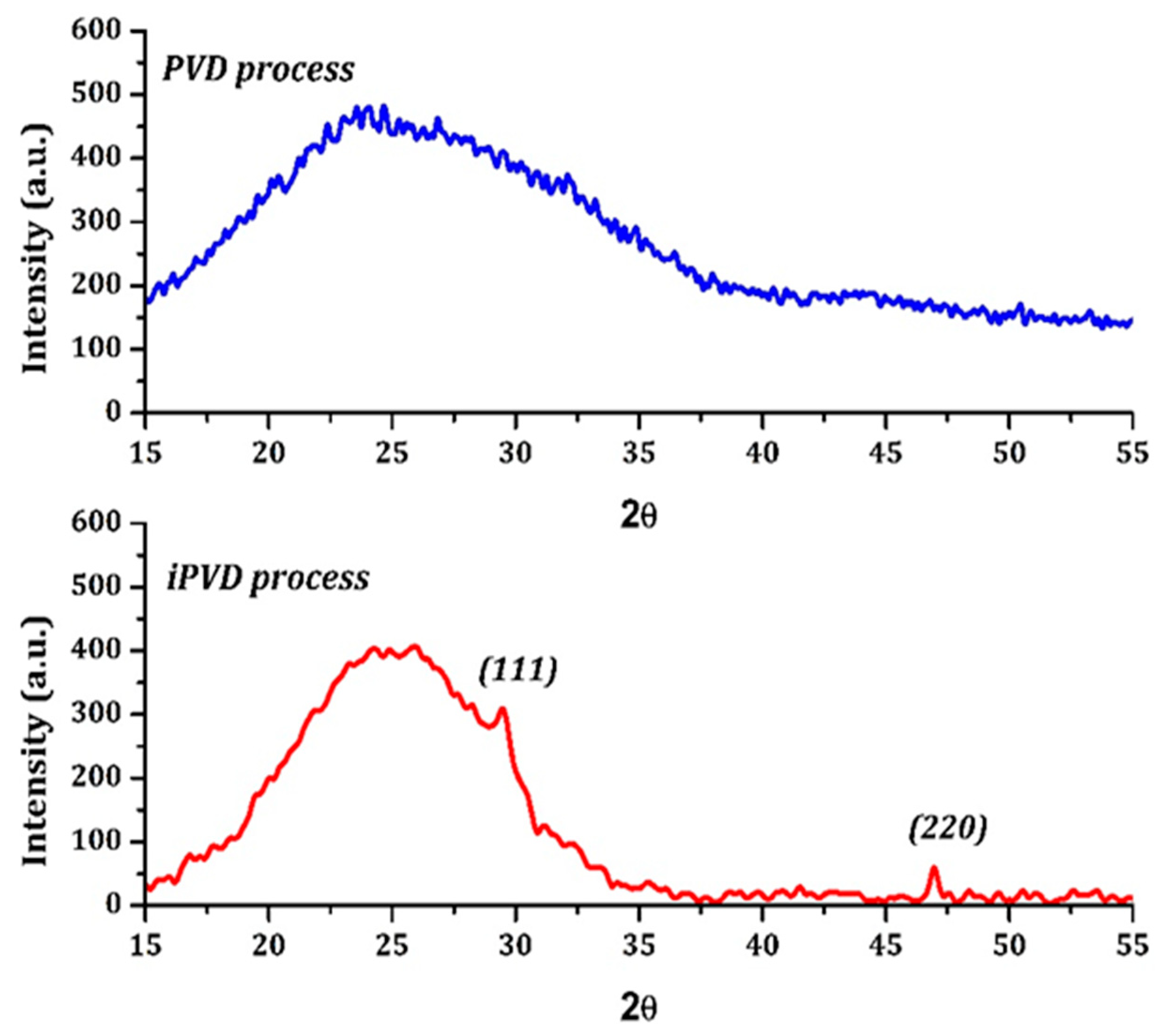
3.1. Structural Analysis

The structural analysis of the Si thin films deposited through the PVD and iPVD processes is shown in Figure 3.
From the XRD microgram, the amorphous nature of the Si thin film is clearly visible for the Si thin film deposited through the PVD process (Figure 3). However, the XRD micrograph for the iPVD process shows the evolution of peaks at 28.5° and 47.3° corresponding to the (111) and (220) planes of Si. It indicates the formation of nano-sized crystallites during the iPVD process [44,45,46]. Similar observations, i.e., the formation of peaks at 2θ = 28.5° and 47.3° for hydrogen additive Argon plasma have been reported by different researchers [47,48]. To determine the grain size from the XRD micrograph, the Scherrer formula [48] is used, which is given below in Equation (1):
D = 0.9 λ β cos θ
where λ = 0.154 nm is the wavelength of the scanning X-ray, θ is the half angle of the diffraction peaks, and β is the full width at half the maximum (FWHM) of the diffraction peak (in radians), which is 0.005 for the (220) plane. The crystal grain size is calculated using Equation (1) by converting the θ value from degrees to radians. In the present work, the grain size is estimated for the (220) plane only and the maximum grain size is around 29 nm. The formation of microcrystallinity in the iPVD process might be associated with the ionization of sputtered Si atoms and the acceleration of the sputtered Si ions due to the sheath electric field formed around the substrate.
In the iPVD process, the sputtered atoms/molecules are ionized before deposition onto the substrate due to the intermediate plasma between the target and the substrate. Considering the acceleration of the positively charged metal ions across the sheath formed near the substrate, the metal ion flux at the substrate can be written as [41]:
Γ M + 0.61 n M +   u B
where
u B = k B T e m M + 1 / 2
is the Bohm velocity, m M + is the metal ion mass, and Te is the electron temperature.
On the other hand, the flux of the neutral metal is determined by the thermal velocity ν M and can be written as
Γ M = 1 4 ν M n M
where
ν M = 8 k B T g Π m M 1 2
is the mean thermal velocity of the gas; mM and Tg are the mass of the neutral atom and the neutral gas temperature, respectively.
Thus,
Γ M + Γ M T e T g 1 2
As in low-pressure plasma, Te is significantly larger than Tg [49,50]. Thus, the fraction of ionized metal flux at the substrate becomes larger in the iPVD process than the fraction of neutral metal in the plasma.
From the electrostatic probe measurement, it is found that the electron temperature during the iPVD process is 1.49 ± 0.09. By substituting the electron temperature value in Equation (4), it is found that the metal ion flux at the substrate is increased proportionally by 7.7 times to the neutral metal flux at the substrate during the iPVD process.
The motion of neutral atoms or molecules cannot be controlled with the help of an external electric field. However, the ion (charge) species can be controlled and collimated by an electric field. In the plasma, a thin positively charged layer known as a sheath is formed near the substrate due to the plasma shielding. Due to the sheath electric field, the ions that enter the sheath region are accelerated towards the substrate and are well-collimated by the sheath’s electric field. Because of this collimation, the ions may reach the bottom of deep narrow trenches or vias, while a neutral flux will tend to deposit on the upper part of the sidewalls leaving the bottom with very little film coverage. Thus, the formation of microcrystallinity of the Si thin films during the iPVD process might be associated with the following factors:
(a)
The deposition flux during the iPVD process consists of more ions than neutrals or ΓM+ > ΓM
(b)
The ions are deposited with higher energy in the iPVD process due to the acceleration by the sheath electric field than the neutrals in the PVD process.
(c)
The ions are collimated by the sheath electric field before the deposition in the iPVD process.

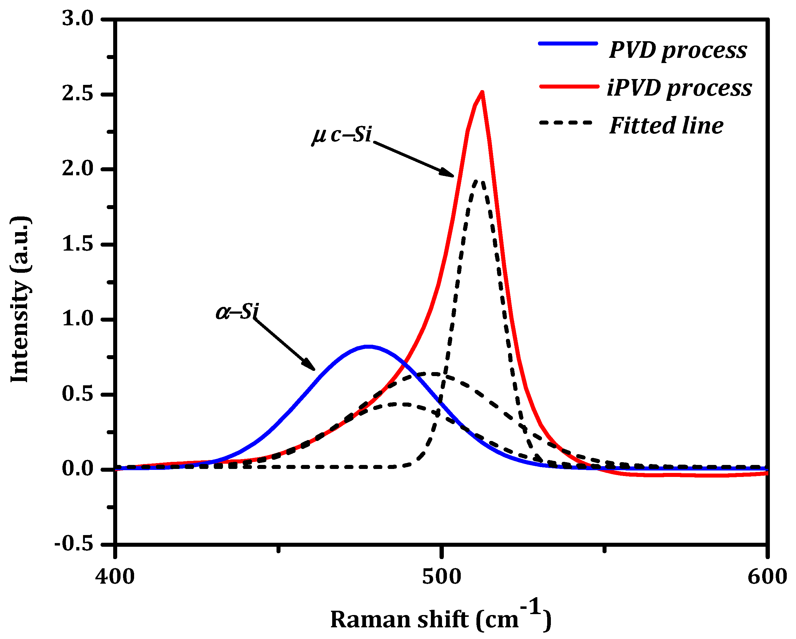
3.2. Raman Spectroscopy

Raman spectroscopy is performed to study the effect of the applied RF field on the structure of the deposited Si thin film. The crystallinity of the films can be estimated from the Raman shift. µc-Si is a mixed-phase material, i.e., it has a number of nano-sized crystallites dispersed in an amorphous phase. Figure 4 shows the Raman spectra for the Si thin films deposited through the PVD and iPVD processes. The Raman peaks are simply observed at 480 cm−1 and 520 cm−1 for amorphous and pure crystalline Si, respectively. The Raman spectra show only a broad hump centered at 480 cm−1 for the a-Si thin film deposited through the PVD process. On the other hand, the Raman spectra for the iPVD sputtered Si thin film show a peak centered at 515 cm−1. The shift in the Raman peak position indicates the formation of crystallites during the iPVD process. This confirms the evolution of a mixed phased µc-Si thin film in the iPVD process. Similar observations were reported by Omid Shekoofa et al. [29] for a µc-Si hydrogenated Si thin film.
The crystallinity fraction is evaluated following the method of deconvolution reported by A. Klossek et al. [48] for the Raman peak of µc-Si:
X c = I 515 + I 496 I 515 + I 496 + I 485
where I515 is the peak intensity of the crystalline peak, I496 corresponds to the peak intensity of the mix phase Si, and I485 corresponds to the peak intensity of amorphous Si [48].
By substituting the intensity values in Equation (5), the crystallization ratio is found to be ~0.7 for the iPVD process in the present experiment. A. Klossek et al. [48] reported that for a µc-Si thin film with a crystallinity above 50%, the grain size becomes ~25 nm. The result shows good agreement with the present experimental results of grain size and crystallinity, estimated using XRD and Raman spectroscopy. The present results confirm the formation of a µc-Si thin film with around 70% crystallinity during the iPVD process.

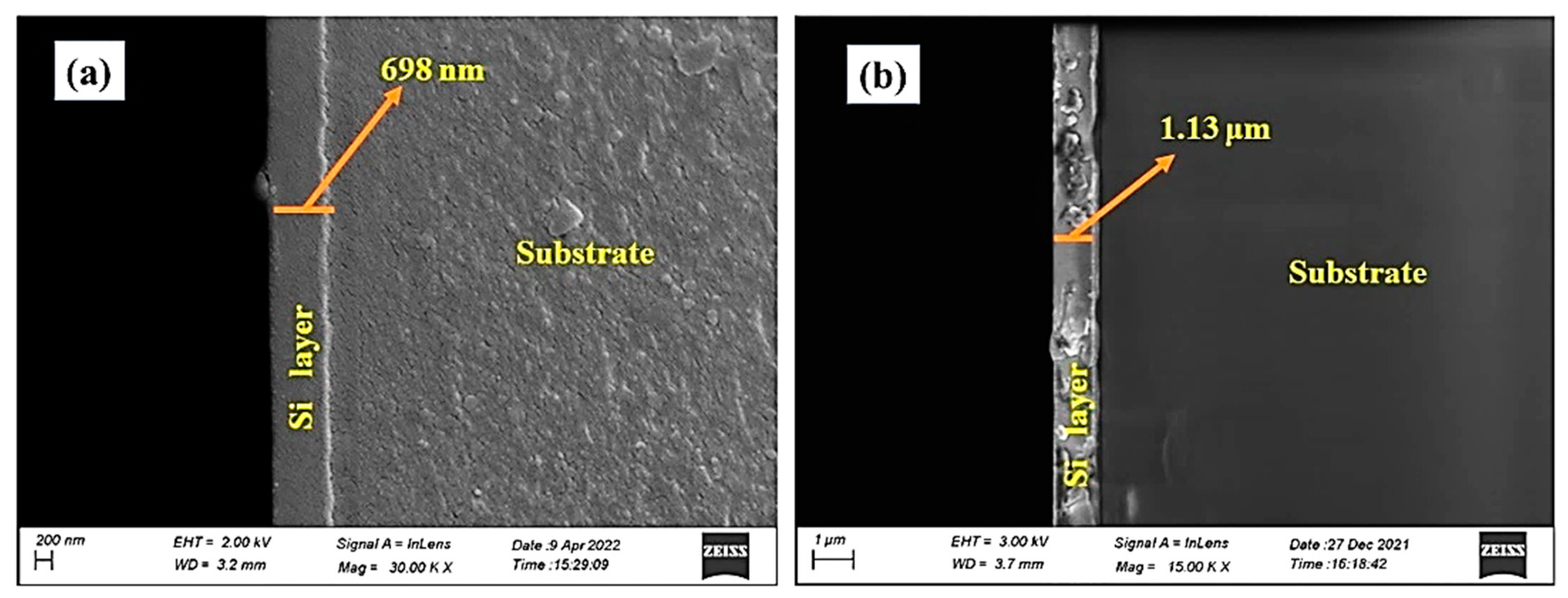
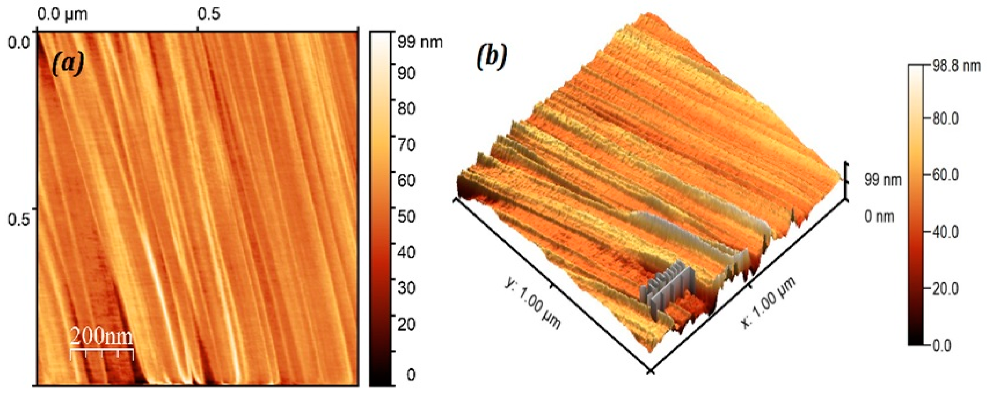
3.3. Morphological Studies

Field emission scanning electron microscopy (FESEM) (Carl ZEISS Gemini, Sigma 300, Germany) is carried out to identify the surface morphology of the Si thin films prepared through the PVD and iPVD processes. Figure 5a shows the surface morphology of a Si thin film prepared through the PVD process and Figure 5b shows the surface morphology of a Si thin film prepared through the iPVD process for two different magnifications.
The FESEM micrographs show very diverse structures for both processes. A granular structure is observed for the PVD process, which is shown in Figure 5a. However, for the iPVD process, a cauliflower-like structure is observed in the FESEM micrographs, which is shown in Figure 5b.
From the FESEM images, it is clearly visible that well-distributed microstructures are elicited in the iPVD process compared to the PVD process. It is observed that the Si thin film prepared through the iPVD process is smoother, dense, and firmly adhered to the substrate. This difference in the surface morphology of the film might be due to the formation of the conglomerated lumps formed during the PVD process, which is not visible in the iPVD process.
To estimate the thickness, the cross-sectional view of the FEMEM image of the Si thin film is analyzed for both the PVD and iPVD processes. It is seen from Figure 6 that the thickness of the thin film is 698.6 nm for the PVD process, whereas the thickness for the iPVD process is 1138.0 nm. In the present work, the deposition time and operating conditions are maintained constant for both the PVD and iPVD processes. The greater thickness of the Si thin film for the iPVD process might be associated with a higher sputtering yield. The sputtering yield in magnetron sputtering depends on the energy of incident ions, and a number of ions impinge on the target materials [51,52]. From the I-V characteristics of the Langmuir probe measurement, it is found that the plasma density for the PVD process is (1.6 ± 0.07) ×1016/m3. In the case of the iPVD process, the plasma density is observed as (6.72 ± 0.41) × 1016/m3. Apart from that the operating DC power during the PVD process, is 125 watts, whereas, for the iPVD process, the operating DC power is 150 watts. The higher discharge power and plasma density for the iPVD process might be responsible for the higher sputtering yield during the iPVD process.
The input power is an important process parameter that affects the deposition rate [53,54]. In the present experiment, it is observed that the deposition rate for the PVD process is 0.38 nm/s, whereas the deposition rate for the iPVD process is 0.63 nm/s. During the PVD process, the operating DC power is 125 watts, whereas, for the iPVD process, the operating DC power is 150 watts. The increase in the deposition rate of the Si thin film for the iPVD process is also associated with the higher operating DC power for the magnetron during the iPVD process. In addition, the increase in the thickness of the Si thin film is also associated with the higher deposition flux due to the ionization of the Si atoms during the iPVD process, as explained in Section 3.1.

3.4. Surface Roughness

Atomic force microscopy (AFM) is used to probe the surface roughness of the Si thin films produced through the PVD and iPVD processes. The surface roughness characterization of the Si thin films is achieved using Gwydion software (Version 2.60). Figure 7 and Figure 8 show the two-dimensional (2-D) and three-dimensional (3-D) images of Si thin films for the PVD and iPVD processes, respectively.
The AFM images suggest a clear change in the surface morphology in both sputtering processes. The roughness profile of the Si thin films prepared through PVD and iPVD processes is shown in Figure 9. The average roughness and the root-mean-square (rms) roughness of the Si thin films for the PVD process are found to be 3.69   nm and 5.25 nm, respectively, whereas, for the iPVD process, the average roughness and the root-mean-square (rms) roughness are found to be 1.84 nm and 2.76 nm. Therefore, more uniform and smoother Si thin films are deposited through the iPVD process compared to the PVD process. The surface roughness typically results in the scattering of electrons or light and, therefore, a ‘‘loss’’ of energy and coherence. The uniformity of the µc-Si thin film plays an important role in multi-junction solar cells [55].

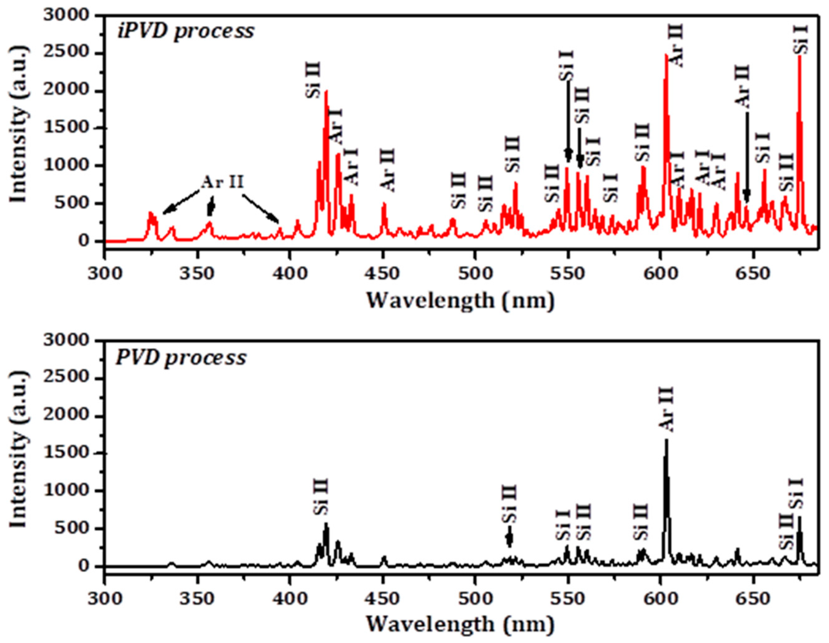
3.5. Optical Emission Spectroscopy (OES) Analysis

OES is a non-interfering process for determining the different species present in the plasma. A qualitative study to investigate the ionization of sputtered Si atoms during the deposition of Si thin films is carried out using an optical emission spectrometer (make: OCEAN OPTICS, model: HR4000). The optical emission spectrum for Argon plasma is recorded for a wavelength range of 200 nm to 1100 nm in both sputtering processes. While investigating the Si spectral lines, the wavelength range of 300 nm to 685 nm is only presented in the present manuscript. Figure 10 shows the spectral line profile for PVD and iPVD processes.
From the observation, more intense atomic and ionic spectral lines of Si are observed for the iPVD process compared to the PVD process. In OES, the higher spectral line intensity indicates a higher concentration of excited atomic or ionic species present in the plasma volume for a constant electron temperature. The presence of more intense ionic spectral lines of Si at 419 nm, 488 nm, 493 nm, 505 nm, 518 nm, 520 nm, 554 nm, 591 nm, and 667 nm for the iPVD process indicates that the fraction of the ionization of sputtered Si atoms in the iPVD process is higher compared to the PVD process.
From Figure 10, it is also seen that there is an increase in the atomic line intensity of Si at 549 nm, 655 nm, and 674 nm during the iPVD process compared to the PVD process. The increase in atomic line intensity for Si might be associated with the higher sputtering yield of Si during the iPVD process compared with the PVD process. The higher sputtering yield for Si during the iPVD process might be associated with the higher plasma density of the Ar plasma that can be visualized for higher spectral intensity for Ar during the iPVD process compared to the PVD process. As a result, the Si thin film’s thickness is increased during the iPVD process in comparison to the PVD process, which is explained in Section 3.3. and shown in Figure 6a,b. In Figure 10, it can be seen that the most intense ionic Si spectral line, observed at 419 nm, is increased by ~4 times during the iPVD process, whereas the most intense atomic Si spectral line, observed at 674 nm, is increased by ~2.5 times during the iPVD process compared to the PVD process. The higher concentration of sputtered Si atoms and dense intermediate plasma increases the ionization probability of Si during the iPVD process. Both ionic and atomic Si species are deposited on the substrate during the iPVD process. However, the deposition flux consists of more ions than neutrals (ΓM+ > ΓM) during the iPVD process.

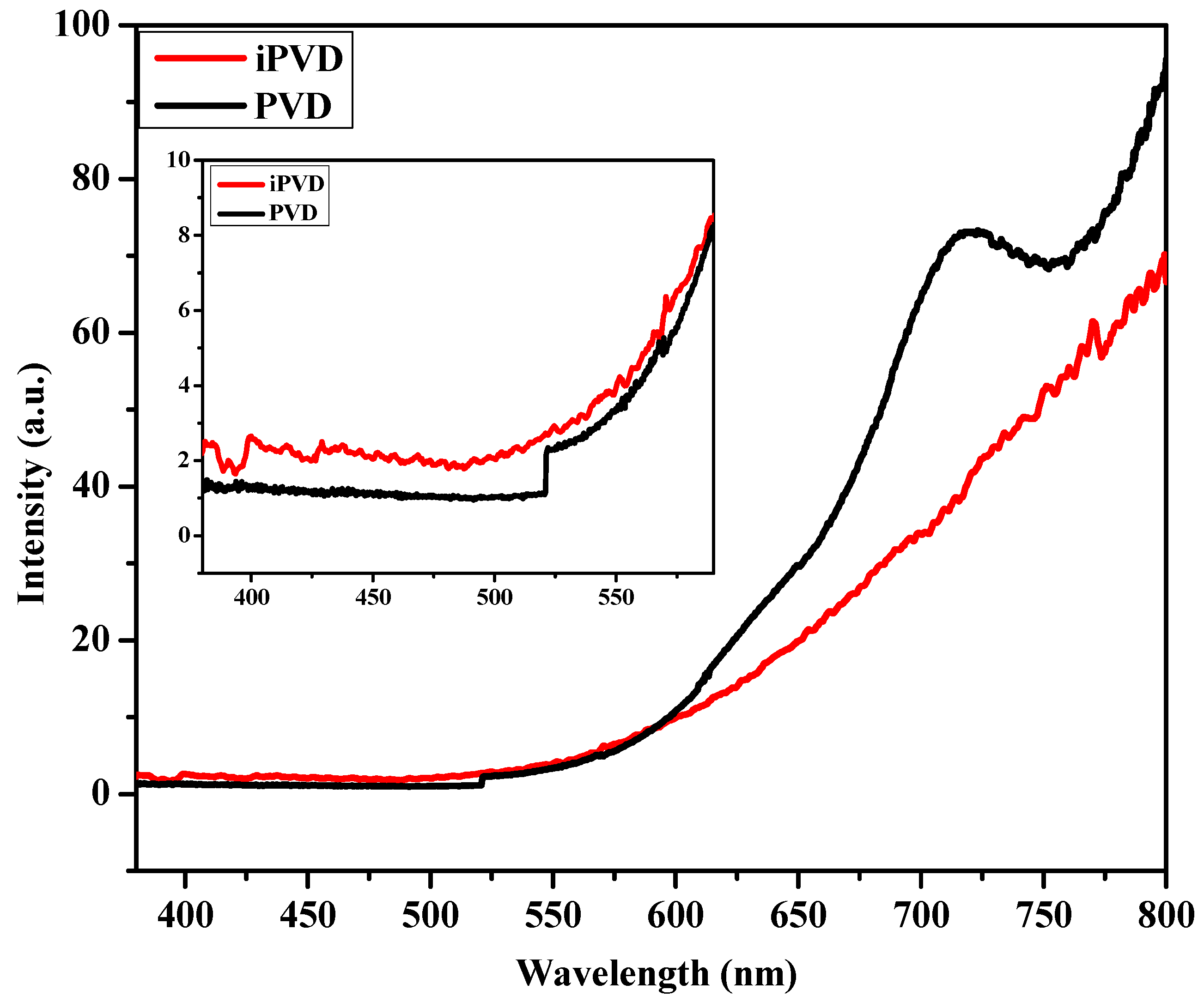
3.6. UV-Visible Spectroscopy

UV-visible spectroscopy is used to study the optical properties of the deposited Si thin films through the PVD and iPVD processes. The optical band gap (Eg) is calculated using Tauc’s equation. Tauc’s equation is used to estimate the band gap energy of semiconductors that can be expressed as follows:
( α h ν ) 1 / γ = B ( h ν E g )
Here, γ is a factor dependent on the nature of the electron transition. The value of γ = ½ is used for direct allowed transitions for a-Si thin films, whereas γ = 2 is used for indirect allowed transitions for μc-Si thin films. The XRD and Raman results confirm the amorphous and microcrystalline nature of Si thin films for the PVD and iPVD processes, respectively; thus, the values γ = ½ and γ = 2 are utilized for the PVD and iPVD processes to estimate the optical band gap in the present work. Figure 11 shows Tauc’s plot for the a-Si (PVD process) and μc-Si (iPVD process) thin films, respectively.
From Tauc’s plot, the value of the Eg for the Si thin films deposited through the PVD and iPVD processes is found to be (1.7 ± 0.08) eV and (1.4 ± 0.05) eV, respectively. The value of the Eg for the PVD process confirms the formation of an a-Si thin film during the PVD process. The decrease in the band gap from (1.7 ± 0.08) eV to (1.4 ± 0.05) eV indicates the successful deposition of a µc-Si thin film during the iPVD process at room temperature. Such µc-Si thin films are used in the bottom cell of multi-junction solar cells due to their long wavelength response [56,57] and can also be used as an infrared sensing device. A similar Eg value for a µc-Si thin film was reported previously by Jarmila Müllerova et al. [58].
The transmittance data for both processes in the visible range are presented in Figure 12. The transmittance is related to the absorbance, as follows:
A = log T %
For clear presentation, an enlarged view of the transmittance plot for the wavelength range 380–590 nm is shown in Figure 12. The transmittance data strongly adhere to the fact that the deposited a-Si thin film has a slightly higher absorbance in the visible range from 400 to 590 nm compared to the µc-Si thin film. Above 590 nm, the transmittance abruptly rises for the a-Si thin film deposited through the PVD process. A relatively low transmittance is observed for the µc-Si thin film deposited through the iPVD process. This also indicates a better probability of absorbance for the µc-Si thin film in the near IR region.

4. Conclusions

The present work describes the formation of a µc-Si thin film at room temperature using the iPVD process. A prominent growth of crystallinity is evident through XRD and Raman spectroscopy. It is found that the crystallite size is around 29 nm for the (220) plane, and the crystallization fraction is ~0.7 for the µc-Si thin film deposited through the iPVD process. From FESEM images, it is found that the a-Si thin films prepared through the PVD process show granular-shaped grains, whereas the µc-Si thin films prepared through the iPVD process reveal a cauliflower-like structure. The AFM observation reveals a prominent decrease in surface roughness for the iPVD process compared to the PVD process. The value of the optical band gap for the Si thin films deposited through the PVD and iPVD processes is found to be 1.7 ± 0.08 eV and 1.4 ± 0.05 eV, respectively. The decrease in the band gap from 1.7 ± 0.08 eV to 1.4 ± 0.05 eV indicates the successful deposition of a µc-Si thin film during the iPVD process at room temperature. The transmittance plot for the µc-Si thin films prepared through the iPVD process confirms the adequate absorption efficiency in the visible and near-infrared regions. The presence of intense ionic spectral lines of Si for the iPVD sputtering process compared to the PVD sputtering process confirms the ionization of sputtered Si atoms in the case of the iPVD process. Thus, the present study indicates that the iPVD process is a feasible method for the deposition of a uniform, dense, microcrystalline Si thin film with higher deposition flux compared to the conventional PVD process. The recent findings will help to develop next-generation flexible electronics including flexible displays and photovoltaic cells at low substrate temperatures. This is the first phase of the experiment to deposit an a-Si thin film using the iPVD process. The influence of the operating pressure, substrate temperature, RF power, mixing of hydrogen gas, etc. on the surface, electrical, optical, mechanical, and wettability properties of Si thin films will be investigated in a phased manner.

Author Contributions

Conceptualization and Methodology: B.K.; Formal Analysis and Investigation: R.S.; Writing—original draft preparation: R.S.; Editing: B.K., M.D. and M.K.M.; Experiment: R.S., S.S., T.H. and T.R.; Data Acquisition: R.S., S.S., T.H., T.R., M.D., S.B. and S.K.; Supervision: B.K. All authors have read and agreed to the published version of the manuscript.

Funding

The authors received no funding during the preparation of the manuscript.

Data Availability Statement

The original contributions presented in the study are included in the article, further inquiries can be directed to the corresponding author.

Acknowledgments

The authors would like to take the opportunity to greatly acknowledge MHRD (Govt. of India), New Delhi and the World Bank for providing financial assistance to establish the experimental set-up under the TEQIP III project. In addition to that, the authors would like to thank the Assam Science and Technology University, Guwahati; the CMP Research Lab, Gauhati University; the Central Instrumentation Facility (CIF), Gauhati University; and IASST, Guwahati for providing the characterization facilities.

Conflicts of Interest

The authors declare no conflict of interest.

References

  1. Takenaka, K.; Setsuhara, Y.; Han, J.G.; Uchida, G.; Ebe, A. Plasma-enhanced reactive linear sputtering source for formation of silicon-based thin films. Rev. Sci. Instrum. 2018, 89, 083902. [Google Scholar] [CrossRef] [PubMed]
  2. Kunii, T.; Mori, K.; Kiriyama, T.; Kitao, J.; Yoshida, N.; Nonomura, S. Resonant photothermal bending spectroscopy at variable temperature 25–150 °C and its application to hydrogenated microcrystalline silicon films. Rev. Sci. Instrum. 2003, 74, 881–883. [Google Scholar] [CrossRef]
  3. Chan, K.Y.; Hashem, E.; Gordijn, A.; Stiebig, H.; Knipp, D. Modelling of contact effects in microcrystalline silicon thin-film transistors. Appl. Phys. A 2009, 96, 751–758. [Google Scholar] [CrossRef]
  4. Schropp, R.E.I. Amorphous (Protocrystalline) and Microcrystalline Thin Film Silicon Solar Cells. In Nanostructured Materials for Solar Energy Conversion; Soga, T., Ed.; Elsevier: Amsterdam, The Netherlands, 2006; pp. 131–166. [Google Scholar]
  5. Shah, A.; Vallat-Sauvain, E.; Torres, P.; Meier, J.; Kroll, U.; Hof, C.; Droz, C.; Goerlitzer, M.; Wyrsch, N.; Vanecek, M. Intrinsic microcrystalline silicon (μc-Si:H) deposited by VHF-GD (very high frequency-glow discharge): A new material for photovoltaics and optoelectronics. Mater. Sci. Eng. B 2000, 69–70, 219–226. [Google Scholar] [CrossRef]
  6. Zhao, Y.; Zhang, X.; Bai, L.; Yan, B. Hydrogenated Amorphous Silicon Thin Film. In Handbook of Photovoltaic Silicon; Yang, D., Ed.; Springer: Berlin/Heidelberg, Germany, 2019; pp. 693–756. [Google Scholar]
  7. Cashmore, J.S.; Apolloni, M.; Braga, A.; Caglar, O.; Cervetto, V.; Fenner, Y.; Goldbach-Aschemann, S.; Goury, C.; Hötzel, J.E.; Iwahashi, T.; et al. Improved conversion efficiencies of thin-film silicon tandem (MICROMORPH™) photovoltaic modules. Sol. Energy Mater Sol. Cells 2016, 144, 84–95. [Google Scholar] [CrossRef]
  8. Zhu, M.; Chen, G.; Chen, P. Green/blue light emission and chemical feature of nanocrystalline silicon embedded in silicon-oxide thin film. Appl. Phys. A 1997, 65, 195–198. [Google Scholar] [CrossRef]
  9. Li, W.; Xia, D.; Wang, H.; Zhao, X.J. Hydrogenated nanocrystalline silicon thin film prepared by RF-PECVD at high pressure. J. Non-Cryst. Solids 2010, 356, 2552–2556. [Google Scholar] [CrossRef]
  10. Schropp, R.E.I. Industrialization of Hot Wire Chemical Vapor Deposition for thin film applications. Thin Solid Film. 2015, 595, 272–283. [Google Scholar] [CrossRef]
  11. Peng, S.; Wang, D.; Yang, F.; Wang, Z.; Ma, F.J. Grown low-temperature microcrystalline silicon thin film by VHF PECVD for thin films solar cell. J. Nanomater. 2015, 327596, 1–5. [Google Scholar] [CrossRef]
  12. Mukhopadhyay, S.; Das, C.; Ray, S.J. Structural analysis of undoped microcrystalline silicon thin films deposited by PECVD technique. J. Phys. D Appl. Phys. 2004, 37, 1736–1741. [Google Scholar] [CrossRef]
  13. Sher, M.J.; Hammond, K.; Christakis, L.; Mazur, E. The photovoltaic potential of femtosecond-laser textured amorphous silicon. In Laser-Based Micro- and Nanopackaging and Assembly VI; Klotzbach, U., Lu, Y., Washio, K., Eds.; SPIE: St. Bellingham, WA, USA, 2013. [Google Scholar]
  14. Adhikari, D.; Junda, M.M.; Sylvain, X.; Collins, R.W.; Podraza, N.J. Nanostructure evolution of magnetron sputtered hydrogenated silicon thin films. J. Appl. Phys. 2017, 122, 075302. [Google Scholar] [CrossRef]
  15. Shekoofa, O.; Wang, J.; Li, D.; Luo, Y. Investigation of Microcrystalline Silicon Thin Film Fabricated by Magnetron Sputtering and Copper-Induced Crystallization for Photovoltaic Applications. Appl. Sci. 2020, 10, 6320. [Google Scholar] [CrossRef]
  16. Matsuda, A.J. Microcrystalline silicon.: Growth and device application. J. Non-Cryst. Solids 2004, 338–340, 1–12. [Google Scholar] [CrossRef]
  17. Shimizu, S.; Matsuda, A.; Kondo, M. Stability of thin film solar cells having less-hydrogenated amorphous silicon i-layers. Sol. Energ. Mater. Sol. Cells 2008, 92, 1241–1244. [Google Scholar] [CrossRef]
  18. Lin, J.; Wu, Z.L.; Zhang, X.H.; Mishra, B.; Moore, J.J.; Sproul, W.D. A comparative study of CrNx coatings Synthesized by dc and pulsed dc magnetron sputtering. Thin Solid Film. 2009, 517, 1887–1894. [Google Scholar] [CrossRef]
  19. Zhang, Q.C. Metal-AlN cermet solar selective coatings deposited by direct current magnetron sputtering technology. J. Phys. D Appl. Phys. 1998, 31, 355–362. [Google Scholar] [CrossRef]
  20. Sproul, W.D.; Graham, M.E.; Wong, M.S.; Lopez, S.; Li, D.J. Reactive direct current magnetron sputtering of aluminum oxide coatings. Vac. Sci. Technol. A 1995, 13, 1188–1191. [Google Scholar] [CrossRef]
  21. Kelesoglu, E.; Mitterer, C. Structure and properties of TiB2 based coatings prepared by unbalanced DC magnetron sputtering. Surf. Coat. Technol. 1988, 98, 1483–1489. [Google Scholar] [CrossRef]
  22. Swann, S. Magnetron sputtering. Phys. Technol. 1988, 19, 67–75. [Google Scholar] [CrossRef]
  23. Tohsophon, T.; Hüpkes, J.; Siekmann, H.; Rech, B.; Schultheis, M.; Sirikulrat, N. High rate direct current magnetron sputtered and texture-etched zinc oxide films for silicon thin film solar cells. Thin Solid Film. 2008, 516, 4628–4632. [Google Scholar] [CrossRef]
  24. Kluth, O.; Rech, B.; Houben, L.; Wieder, S.; Schöpe, G.; Beneking, C.; Wagner, H.; Löffl, A.; Schock, H.W. Texture etched ZnO:Al coated glass substrates for silicon based thin film solar cells. Thin Solid Film. 1999, 351, 247–253. [Google Scholar] [CrossRef]
  25. Ou, Y.X.; Ouyang, X.P.; Liao, B.; Zhang, X.; Zhang, S. Hard yet tough CrN/Si3N4 multilayer coatings deposited by the combined deep oscillation magnetron sputtering and pulsed dc magnetron sputtering. Appl. Surf. Sci. 2020, 502, 144168. [Google Scholar] [CrossRef]
  26. Batan, A.; Franquet, A.; Vereecken, J.; Reniers, F. Characterisation of the silicon nitride thin films deposited by plasma magnetron. Surf. Interface Anal. 2008, 40, 754–757. [Google Scholar] [CrossRef]
  27. Fthenakis, V.M.; Moskovitz, P.D. An assessment of silane hazards. Solid State Technol. 1990, 33, 81–85. [Google Scholar]
  28. Van Ommeren, J. Silane gas venting/treatment lessons learned and best practices. Process. Saf. Prog. 2011, 30, 104–114. [Google Scholar] [CrossRef]
  29. Khelifati, N.; Tata, S.; Rahal, A.; Cherfi, R.; Fedala, A.; Kechouane, M.; Mohammed-Brahim, T. The annealing temperature effecton the electrical properties of boron-doped hydrogenated amorphous silicon a-Si:H(B). Phys. Status Solidi 2010, C7, 679–682. [Google Scholar] [CrossRef]
  30. El Whibi, S.; Derbali, L.; Tristant, P.; Jaoul, C.; Colas, M.; Mayet, R.; Cornette, J.; Ezzaouia, H. Optimized nc-Si:H thin films with enhanced optoelectronic properties prepared by micro-waves PECVD used as an effective silicon surface passivation layer. J. Mater. Sci. Mater. Electron. 2019, 30, 2351–2359. [Google Scholar] [CrossRef]
  31. Yue, H.; Wu, A.; Zhang, X.; Li, T. New two-step growth of microcrystalline silicon thin films without incubation layer. J. Cryst. Growth. 2011, 322, 1–5. [Google Scholar] [CrossRef]
  32. Layadi, N.; Cabarrocas, P.R.I.; Drevillon, B. Real-time spectroscopic ellipsometry study of the growth of amorphous and microcrystalline silicon thin films prepared by alternating silicon deposition and hydrogen plasma treatment. Phys. Rev. B 1995, 52, 5136–5143. [Google Scholar] [CrossRef] [PubMed]
  33. Sharma, P.; Tripathi, N.; Gupta, N. Nanocrystalline silicon thin film prepared by e-beam evaporation for display application. J. Mater. Sci. Mater. Electron. 2017, 28, 3891–3896. [Google Scholar] [CrossRef]
  34. Wang, L.-Q.; Wang, W.-Y.; Huang, J.-H.; Tan, R.-Q.; Song, W.J.; Chen, J.-M. Growth and properties of hydrogenated microcrystalline silicon thin films prepared by magnetron sputtering with different substrate temperatures. Rare Met. 2022, 41, 1037–1042. [Google Scholar] [CrossRef]
  35. Konstantinidis, S.; Nouvellon, C.; Dauchot, J.P.; Wautelet, M.; Hecq, M. RF amplified magnetron source for efficient titanium nitride deposition. Surf. Coat. Technol. 2003, 174–175, 100–106. [Google Scholar] [CrossRef]
  36. Alami, J.; Persson, P.O.; Music, D.; Gudmundsson, J.T.; Bohlmark, J.; Helmersson, U. Ion-assisted physical vapor deposition for enhanced film properties on nonflat surfaces. J. Vac. Sci. Technol. A 2005, 23, 278–280. [Google Scholar] [CrossRef]
  37. Li, N.; Allain, J.P.; Ruzic, D.N. Enhancement of aluminum oxide physical vapor deposition with a secondary plasma. Surf. Coat. Technol. 2002, 149, 161–170. [Google Scholar] [CrossRef]
  38. Matsuda, Y.; Koyama, Y.; Tashiro, K.; Fujiyama, H. MgO deposition using reactive ionized sputtering. Thin Solid Film. 2003, 435, 154–160. [Google Scholar] [CrossRef]
  39. Matsuda, Y.; Iwaya, M.; Koyama, Y.; Shinohara, M.; Fujiyama, H. Effect of inductively-coupled plasma assist on the crystal orientation of magnesium oxide thin films produced by reactive sputtering. Thin Solid Film. 2004, 457, 64–68. [Google Scholar] [CrossRef]
  40. Schneider, J.M.; Sproul, W.D.; Voevodin, A.A.; Matthews, A. Crystalline alumina deposited at low temperatures by ionized magnetron sputtering. J. Vac. Sci. Technol. A 1997, 15, 1084–1088. [Google Scholar] [CrossRef]
  41. Helmersson, U.; Lattemann, M.; Bohlmark, J.; Ehiasarian, A.P.; Gudmundsson, J.T. Ionized physical vapor deposition (IPVD): A review of technology and applications. Thin Solid Film. 2006, 513, 1–24. [Google Scholar] [CrossRef]
  42. Bohlmark, J.; Östbye, M.; Lattemann, M.; Ljungcrantz, H.; Rosell, T.; Helmersson, U. Guiding the deposition flux in an ionized magnetron discharge. Thin Solid Film. 2006, 515, 1928–1931. [Google Scholar] [CrossRef]
  43. Shin, K.S.; Sahu, B.B.; Kumar, M.; Leksakul, K.; Han, J.G. Tailoring of microstructure in hydrogenated nanocrystalline Si thin films by ICP-assisted RF magnetron sputtering. J. Phys. D Appl. Phys. 2015, 48, 475303. [Google Scholar] [CrossRef]
  44. Vasques, A.L.Q.; Torchynska, T.V.; Polupan, G.; Matsumoto-Kuwabara, Y.; Khomenkova, L.; Shcherbyna, L.V. Size Dependent Photoluminescence of Si Nano-Crystals Embedded in Amorphous Silicon. Solid State Phenom. 2008, 131–133, 71–76. [Google Scholar]
  45. Hsin-Ying, L.; Ting-Chun, W.; Chun-Yen, T. Performance Improvement of Microcrystalline p-SiC/i-Si/n-Si Thin Film Solar Cells by Using Laser-Assisted Plasma Enhanced Chemical Vapor Deposition. Int. J. Photoenergy 2014, 2014, 795152. [Google Scholar]
  46. Moreno, M.; Boubekri, R.; Cabarrocas, P.R.I. Study of the effects of different fractions of large grains of μc-Si: H: F films on the infrared absorption on thin film solar cells. Sol. Energy Mater. Sol. Cells 2012, 100, 16–20. [Google Scholar] [CrossRef]
  47. Elsholz, F.; Schöll, E.; Rosenfeld, A. Control of surface roughness in amorphous thin-film growth. Appl. Phys. Lett. 2004, 84, 4167–4169. [Google Scholar] [CrossRef]
  48. Klossek, A.; Mankovics, D.; Arguirov, T.; Ratzke, M.; Kirner, S.; Friedrich, F.; Gabriel, O.; Stannowski, B.; Schlatmann, R.; Kittler, M. Growth process of microcrystalline silicon studied by combined photoluminescence and Raman investigations. J. Appl. Phys. 2013, 114, 223511. [Google Scholar] [CrossRef]
  49. Kakati, B.; Kausik, S.S.; Bandyopadhyay, M.; Saikia, B.K.; Kaw, P.K. Development of a novel surface assisted volume negative hydrogen ion source. Sci. Rep. 2017, 7, 11078. [Google Scholar] [CrossRef] [PubMed]
  50. Kakati, B.; Kausik, S.S.; Bandyopadhyay, M.; Saikia, B.K.; Saxena, Y.C. Effect of argon addition on plasma parameters and dust charging in hydrogen plasma. J. Appl. Phys. 2014, 116, 163302. [Google Scholar] [CrossRef]
  51. Nisha, N.; Sahu, B.B. Overall aspect for designing magnetron sputtering plasma sources and their applications in the deposition of ITO films. AIP Adv. 2024, 14, 050702. [Google Scholar] [CrossRef]
  52. Mahne, N.; Čekada, M.; Panjan, M. Total and differential sputtering yields explored by SRIM simulations. Coatings 2022, 12, 1541. [Google Scholar] [CrossRef]
  53. Ferreira, F.; Serra, R.; Oliveira, J.C.; Cavaleiro, A. Effect of peak target power on the properties of Cr thin films sputtered by HiPIMS in deep oscillation magnetron sputtering (DOMS) mode. Surf. Coat. Technol. 2014, 258, 249–256. [Google Scholar] [CrossRef]
  54. Shi, W.; Peng, J.; Xu, Z.; Shen, Q.; Wang, C. Effect of power on structural and mechanical properties of DC magnetron sputtered Cr coatings. Metals 2023, 13, 691. [Google Scholar] [CrossRef]
  55. Ren, H.; Zhao, Y.; Zhang, X.D.; Ge, H.; Wang, Z.P. Microcrystalline silicon thin films and triple-junction solar cells. Adv. Mater. Res. 2012, 468–471, 1912–1915. [Google Scholar] [CrossRef]
  56. Lee, C.-H.; Shin, M.; Lim, M.-H.; Seo, J.-Y.; Lee, J.-E.; Lee, H.-Y.; Kim, B.-J.; Choi, D. Material properties of microcrystalline silicon for solar cell application. Sol. Energy Mater. Sol. Cells 2011, 95, 207–210. [Google Scholar] [CrossRef]
  57. Yan, B.; Yue, G.; Yang, J.; Banerjee, A.; Guha, S. Hydrogenated microcrystalline silicon single-junction and multi-junction solar cells. Mater. Res. Soc. Symp. Proc. 2003, 762, A4.1.1–A4.1.12. [Google Scholar] [CrossRef]
  58. Müllerova, J.; Šutta, P.; Holá, M. Optical absorption in Si: H thin films: Revisiting the role of the refractive index and the absorption coefficient. Coatings 2021, 11, 1081. [Google Scholar] [CrossRef]
Figure 1. Schematic diagram of the experimental setup.
Crystals 15 00106 g001
Figure 2. Pictorial representation of (a) the PVD process and (b) the iPVD process.
Crystals 15 00106 g002
Figure 3. XRD pattern for PVD and iPVD sputtered Si thin film.
Crystals 15 00106 g003
Figure 4. Raman spectra of PVD and iPVD sputtered Si thin films.
Crystals 15 00106 g004
Figure 5. FESEM images of Si thin films through (a) the PVD process and (b) the iPVD process.
Crystals 15 00106 g005
Figure 6. Cross-sectional view of the Si thin film for (a) the PVD process and (b) the iPVD process.
Crystals 15 00106 g006
Figure 7. (a) 2-D and (b) 3-D AFM images of Si thin film for PVD process.
Crystals 15 00106 g007
Figure 8. (a) 2-D and (b) 3-D AFM images of Si thin film for the iPVD process.
Crystals 15 00106 g008
Figure 9. Roughness profile for PVD and iPVD processes.
Crystals 15 00106 g009
Figure 10. Spectral line profile for PVD and iPVD processes.
Crystals 15 00106 g010
Figure 11. Tauc’s plot for PVD and iPVD processes.
Crystals 15 00106 g011
Figure 12. Transmittance plot for PVD and iPVD processes (enlarged view for 380 nm to 590 nm is shown in inset).
Crystals 15 00106 g012
Table 1. Different processes used for the deposition of crystalline Si thin films.
Sl. No.Deposition TechniqueSubstrate Temperature (°C)Post Annealing (°C)Silane Gas UsedHydrogen Gas UsedCrystallization Fraction (%)
1Microwave plasma-enhanced chemical vapor deposition (MW-PECVD) [30]250NoYesYes~91
2Electron cyclotron resonance plasma-enhanced chemical vapor deposition (ECR-PECVD) [31]250NoYesYes22.9 to 50.6
3Capacitively coupled rf (13.56 MHz) glow discharge system [32]250NoYesYes64
4E-beam evaporation technique [33]90300No-Crystalline
5RF (13.56 MHz) magnetron sputtering [34]100–300NoNoYes~49.2% to ~61.0%.
6Ionized physical vapor deposition (Present work)Room temperatureNoNoNo~70%
Table 2. The deposition parameters for the Si thin film preparation.
Si DepositionSputtering ProcessSubstrate TemperatureOperating Pressure (MBAR)Ar flow Rate (SCCM)DC Discharge Voltage/Discharge CurrentRF Power (W)
Sample 1PVD (DC)Room temperature 2.5 × 10 3 35500 volt/250 mA0
Sample 2iPVD (RF-DC)Room temperature 2.5 × 10 3 35500 volt/300 mA250
Disclaimer/Publisher’s Note: The statements, opinions and data contained in all publications are solely those of the individual author(s) and contributor(s) and not of MDPI and/or the editor(s). MDPI and/or the editor(s) disclaim responsibility for any injury to people or property resulting from any ideas, methods, instructions or products referred to in the content.

