Article

Simulation-Based Studies on FAGeI3-Based Lead (Pb2+)-Free Perovskite Solar Cells

1
School of Mechanical Engineering, Yeungnam University, Gyeongsan 38541, Republic of Korea
2
School of Materials Science and Engineering, Yeungnam University, Gyeongsan 38541, Republic of Korea
3
Department of Chemistry, College of Science, King Saud University, Riyadh 11451, Saudi Arabia
4
Department of Chemistry, Indian Institute of Technology Indore, Simrol 600036, MP, India
*
Authors to whom correspondence should be addressed.
These authors contributed equally to this work.
Crystals 2025, 15(2), 135; https://doi.org/10.3390/cryst15020135
Submission received: 8 January 2025 / Revised: 23 January 2025 / Accepted: 24 January 2025 / Published: 26 January 2025
(This article belongs to the Section Materials for Energy Applications)

Abstract

:
In the recent reports, it is clear that lead-free perovskite materials with low band gaps are desirable candidates for photovoltaic cells. In this regard, it was observed that germanium (Ge) is a less toxic lead-free metal that is significant for the preparation of Ge-based perovskite materials. Ge-based perovskite materials, for example, methyl ammonium germanium iodide (MAGeI3), cesium germanium iodide (CsGeI3), and/or formamidinium germanium iodide (FAGeI3) may be the suitable absorber materials and alternatives towards the fabrication of lead-free photovoltaic cells. In the past few years, few attempts were made to develop FAGeI3-based perovskite solar cells, but their photovoltaic performance is still under limitations. This is indicating that some significant and effective strategies should be designed and developed for the construction of Ge-based perovskite solar cells. It is believed that optimization of layer thickness, device structure, and selection of a suitable electron transport layer (ETL) may improve the photovoltaic performance of FAGeI3-based perovskite solar cells. Solar cell capacitance simulation, i.e., SCAPS is one of the promising software programs that can provide significant theoretical findings for the development of FAGeI3-based perovskite solar cells. The simulation studies via SCAPS may benefit researchers to save their energy and high cost for the optimization process in the laboratories. In this research article, SCAPS was adopted as a simulation tool for the theoretical investigations of FAGeI3-based perovskite solar cells. The simulation studies exhibited the excellent efficiency of 15.62% via SCAPS. This study proposed the optimized device structure of FTO/TiO2/FAGeI3/PTAA/Au with enhanced photovoltaic performance.

1. Introduction

In the present time, energy is the basic underpinning of economic progress, human civilization, and the three pillars of the twenty-first century, i.e., energy, information, and material [1,2,3]. The conventional approaches/sources, which include coal, natural gas, and oil, are limited and experiencing severe scarcity [4,5,6,7]. Therefore, as a result, strengthening the energy structure, ensuring a sustainable energy supply, and finding and using new energies or resources has become a major task [8,9,10]. Although various energy technologies and resources, such as energy storage and energy conversion, have been developed to fight the energy crisis [11,12,13]. But solar energy has become one of the most recognized neat and clean energy sources, which could be useful to overcome the energy crisis in the future [8,9,10,11,12,13]. Solar energy needs to be converted to electrical energy by employing photovoltaic cells, which are also called solar cells. In this context, traditional solar cells, such as silicon solar cells, were developed and have been commercialized [14,15,16]. Unfortunately, the complicated manufacturing process and high cost of the traditional solar cells are some of the challenges for the scientific community. Researchers are working hard towards the fabrication and development of low-cost, simple fabrication-processed, and highly efficient solar cells. In this connection, dye-sensitized solar cells [17], organic solar cells [18], perovskite solar cells (PSCs) [19], polymer-based solar cells [20], quantum dot solar cells [21], and bulk hetero-junction solar cells [22] have been designed and reported. Among the reported solar cells, PSCs have been shined as a rising star in the field of thin-film solar cell technology due to their excellent efficiency, low cost, and simple fabrication methods [23]. It is to be noted that PSCs have different components that are known as absorber material, electron transport material (ETM), hole transport material (HTM), and metal contacts. The absorber materials are the perovskite materials with narrow band gaps that have the potential to absorb the sunlight.
In 2009, perovskite absorber materials were first adopted as visible light sensitizers in the construction of dye-sensitized solar cells, which demonstrated decent significant findings towards photovoltaic technology [24]. This work by Kojima et al. [24] opened the door for the researchers towards the development of next-generation thin-film photovoltaic cells with such an excellent absorber material. The general perovskite molecular structure can be illustrated as below:
AMX3
(In the above formula, A = methyl ammonium (CH3NH3+ = MA), cesium (Cs+), or formamidinium (NH2CHNH2+ = FA), M= lead (Pb2+), germanium (Ge2+), tin (Sn2+) and X = halide anions such as I, Cl, or Br). The published reports on PSCs suggested that Pb2+-based perovskite materials-based solar cells are a promising thin-film photovoltaic technology because of their excellent performance and cost-effectiveness [24]. The Pb2+ absorber materials-based PSCs demonstrated excellent power conversion efficiency, e.g., PCE of more than 25% [25]. This is suggesting that Pb2+-based absorber materials are promising photovoltaic candidates, but the presence of the toxic nature of Pb2+ remains a challenge for the scientific community [26]. Thus, researchers moved towards the design and fabrication of Pb2+-free PSCs by utilizing Pb2+-free absorber materials. Previously, various research groups employed different Pb2+-free perovskite materials for photovoltaic applications. Pb2+-free perovskites materials with less toxic or non-toxic metals such as bismuth (Bi) [27], tin (Sn) [28], antimony (Sb) [29], and germanium (Ge) [30] have been studied for the development of PSCs. It was observed that Sn-containing perovskite materials have low band gaps and have been successfully utilized in Pb2+-free PSCs, and decent efficiency of more than 13% was achieved [31]. Although Bi- and Sb-based perovskite-like materials have been widely used in the fabrication of Pb2+-free PSCs [32], it has now been observed that Bi-containing phases are now the subject of considerable research, with applications in optoelectronic applications such as photodetectors or hydrogen production rather than photovoltaics [33,34,35]. This is due to a wide band gap and poor morphological features. In further studies, Ge-based absorber materials show significant roles for PSC applications, and their experimental studies are still under investigation [36]. It is believed that we may expect a surge in the construction of Ge-based PSCs in the next few years. Ge is a plentiful metal with less toxicity and environmental issues when compared to Pb2+ [37]. Thus, it is of great significance to explore Ge-based absorber materials for PSCs. In this regard, MAGeI3, CsGeI3, and FAGeI3 have been explored for thin film PSCs [37,38,39,40]. In particular, FAGeI3 has decent photovoltaic properties, and only a few reports are available on the use of FAGeI3 as an absorber material for solar cell applications [41]. The efficiency of FAGeI3-based PSCs is still lower than that of Pb2+-based solar cells. Thus, it is required to design and optimize various parameters and fabrication procedures for the enhancement of the efficiency of Ge-based PSCs.
In the last 5 years, a promising simulation tool based on solar cell capacitance has been widely used for the theoretical study of PSCs [42,43,44,45,46,47,48]. This software named SCAPS displayed various promising and optimized conditions for the development of PSCs. It is understood that the efficiency of the PSCs is largely influenced by the device structure, type and thickness of the ETL, light absorber layer, and HTL. Hence, it may be expected that the efficiency of FAGeI3-based PSCs can be further enhanced by optimizing different parameters and conditions. The SCAPS may be a promising tool to provide the optimized conditions for researchers towards the construction of FAGeI3-based devices.
Herein, report the numerical simulation investigations by employing FAGeI3 as absorber material and different ETLs and HTLs were adopted to find the most suitable and efficient ETL and HTL for FAGeI3-based PSCs. We have also varied the thickness of the absorber layer, HTL, and ETL to achieve the highest PCE value of the simulated device. The obtained results via SCAPS showed that FTO/TiO2/FAGeI3/PTAA/Au is the most efficient device configuration, which displayed an excellent PCE of 15.62%. We believe that the proposed device configuration may be beneficial for the researchers towards the manufacturing of FAGeI3-based PSC devices.

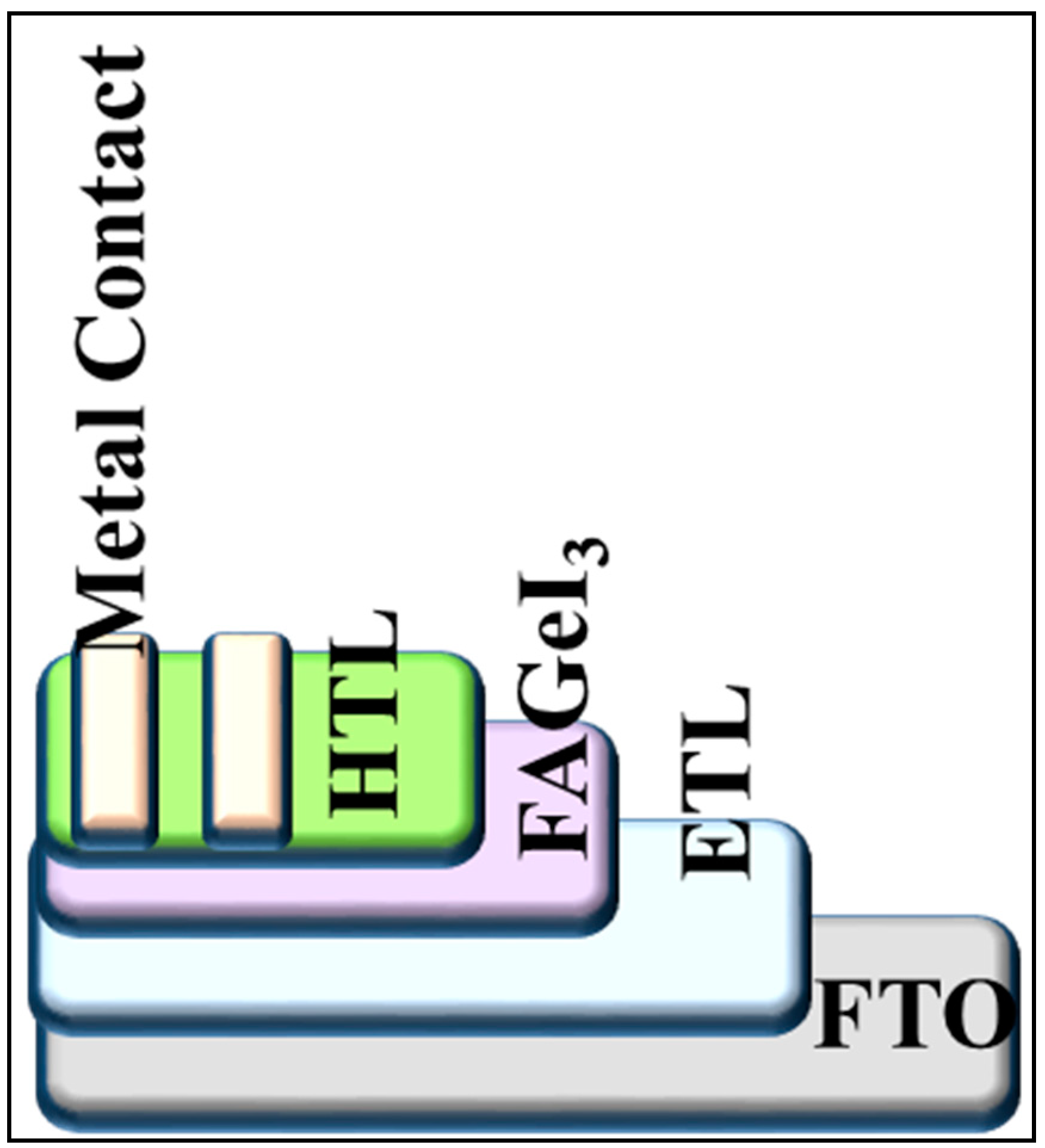
2. Device Structure and Simulation

In this study, we adopted SCAPS simulation software for the theoretical investigations of FAGeI3-based PSCs. The SCAPS was developed by Prof. Marc Burgelman for the simulation of thin film solar cells [49]. Nowadays, SCAPS is widely used for PSC studies. Thus, we have also employed SCAPS for the theoretical studies of Pb2+-free PSCs. Initially, we have adopted the device structure of FTO/ETL/FAGeI3/HTL/Au for simulation studies. Furthermore, SCAPS was open, and the above device configuration was set. The parameters, such as band gap, electronegativity, electron affinity, thickness, defect density, and many more, were adopted from the reported literature and input in the SCAPS software for FTO, absorbers, ETL, and HTL. The device configuration of the Pb2+-free PSCs has been displayed in Scheme 1.
Furthermore, SCAPS was run for device configuration of FTO/ETL/FAGeI3/HTL/Au under illumination of AM 1.5 G (100 mW/cm2; temperature = 300 K) and photocurrent density versus voltage (JV). Graphs were obtained that demonstrated photocurrent density (Jsc), open circuit voltage (Voc), fill factor (FF), and PCE. It is to state that SCAPS software worked on the principle of Poisson’s and continuity equations. The Poisson’s and continuity equations can be explained as given below,
2ψ = q/ε (n − p + NA − ND)
(Herein, ND = donor concentration; NA = acceptor concentration, whereas ψ is electrostatic potential).
The continuity equations have been provided below,
∇.Jn − q ∂n/∂t = +qR
∇.JP + q ∂p/∂t = −qR
(In above equations, Jp = holes current density, Jn=electrons current density, whereas R = carrier recombination rate).
The drift diffusion current relations can be illustrated by the given equations below,
Jn = qnµnE + qDn ∇n
Jp = qpµpE − qDp
(where Dn is the electron diffusion coefficient, while Dp is the hole diffusion coefficient).
The used values for the dielectric permittivity, band gap, electron affinity, etc., for FAGeI3, ETLs, and HTLs have been taken from the reported literature and summarized in Table 1, Table 2 and Table 3. The values of the parameters for different layers, such as the absorber layer, ETL, and HTL, were adopted from previous studies with some modifications [13,43,44,45,46,47,48].

3. Results and Discussion

3.1. Optimization of FAGeI3 Layer

In the first simulation test, tin oxide (SnO2) was adopted as ETL, and spiro-OMeTAD was used as HTL. The thickness of the ETL was used as 50 nm, whereas the thickness of the HTL was used as 100 nm, and the absorber layer thickness was 50 nm. The SCAPS was run to obtain the JV results under 1 sun conditions (AM 1. 5 G; 100 mW/cm2). Figure 1 shows the collected JV data of the device configuration of FTO (500 nm)/SnO2 (50 nm)/FAGeI3 (50 nm)/spiro-OMeTAD (100 nm). It was observed that simulation for a 50 nm absorber layer-based device configuration exhibits a low Jsc value of approximately 3.48 mA/cm2 with an excellent Voc of 1.28 V. The lower Jsc value may be due to the generation of fewer charge carriers (electron-hole) in the FAGeI3 layer. Thus, a lower PCE of 3.85% was obtained for 50 nm thick absorber layer-based Pb2+-free PSCs.
The thickness of the absorber layer may play a crucial role in the improvement in the photovoltaic performance of the proposed device configuration. Thus, it was considered that optimization of absorber layer thickness is of great importance for further simulation studies. In this regard, the thickness of the FAGeI3 layer was tuned in the range of 50 nm to 1000 nm. The SCAPS software (3.3.10) was run under similar conditions except for the change in the thickness of the absorber layer. The collected JV results from the simulation studies are shown in Figure 2a. It was observed from the JV data that Jsc value increases with increasing thickness of the FAGeI3 layer. This may be due to the generation of more photons with a higher thickness of the FAGeI3 layer. Thus, more photons lead to the generation of more Jsc value as shown in Figure 2b. The Voc value increases when the thickness of FAGeI3 increases from 150 nm to 700 nm. However, the FF decreases with increasing thickness of FAGeI3.
In contrast, the PCE of the simulated device increases with increasing thickness of the FAGeI3 layer (Figure 2b). The PCE of 3.85%, 8.63%, 12.39%, 14.57%, 15.46%, and 15.83% were obtained for 50 nm, 150 nm, 300 nm, 500 nm, 700 nm, and 1000 nm thick FeGeI3 layer-based Pb2+-free PSCs, respectively. We believe that a 1000 nm thick layer would be insignificant in real-time device fabrication. Moreover, a small difference was observed in the PCE of 700 nm and 1000 nm thick absorber layer-based simulation studies. Thus, by considering this, we have used a 700 nm thick absorber layer for further simulation examinations.

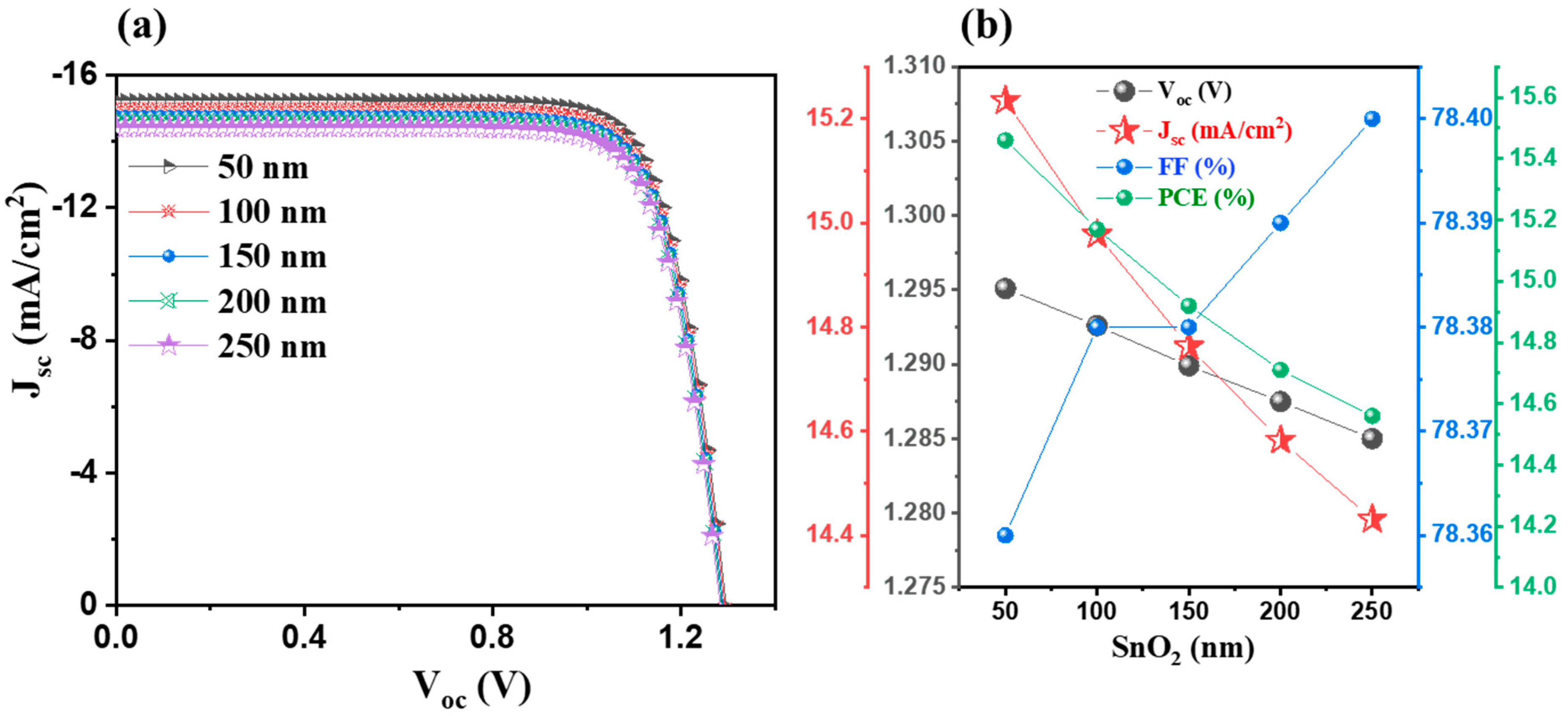
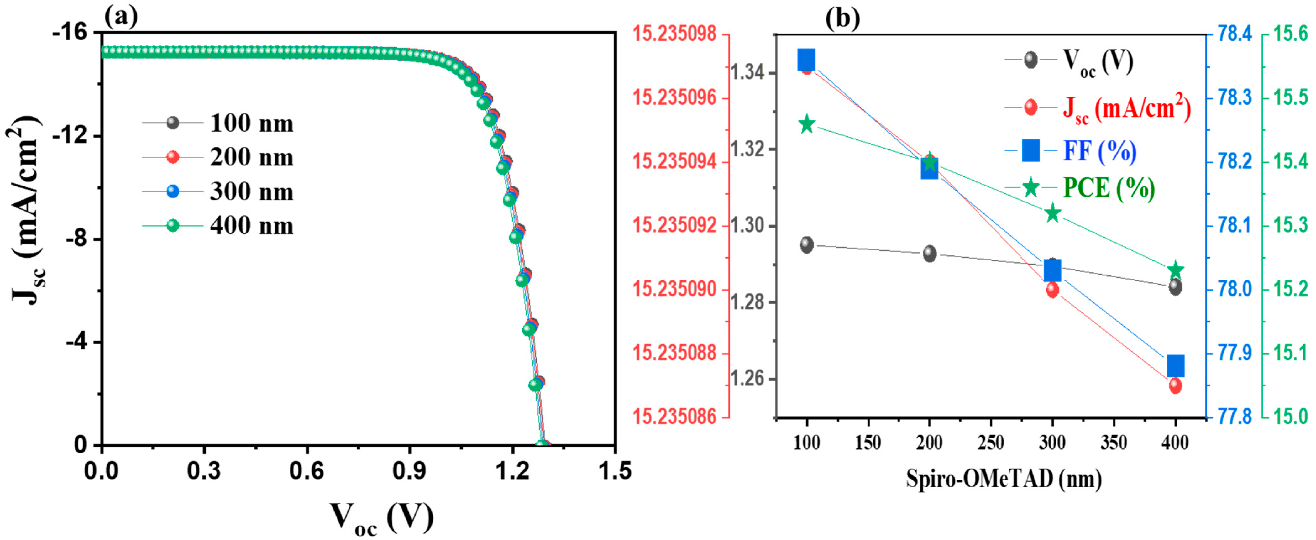
3.2. Effects of Thickness of ETL and HTL

The thickness of the absorber layer affects the performance of the PSCs more significantly compared to the ETL or HTL layer. However, it is also important that we can neglect the effects of the thickness of ETL and HTL. Therefore, we have changed the thickness of SnO2 ETL in the range of 50 to 250 nm, whereas the thickness of HTL was fixed at 100 nm and FAGeI3 at 700 nm. The simulated results were collected in the form of JV data, which are demonstrated in Figure 3a. It was seen from the JV results that the highest Voc value was observed for the 50 nm thick SnO2 layer, whereas the lowest Voc was observed for the 250 nm thick SnO2 layer (Figure 3b).
Similarly, the lowest Jsc was obtained at 250 nm, and the highest Jsc was observed at the 50 nm thick SnO2 layer. Thus, PCE of 15.46%, 15.17%, 14.92%, 14.71%, and 14.56% was obtained for 50 nm, 100 nm, 150 nm, 200 nm, and 250 nm thick SnO2 layer-based PSCs, respectively. Thus, it is worthy to mention that a 50 nm thick ETL would be useful for the simulation of FAGeI3-based PSCs. Therefore, we fixed a 50 nm thickness for the SnO2 layer, whereas for the FAGeI3 layer, we fixed a 700 nm thickness, but the thickness of spiro-OMeTAD was varied in the range of 100 to 400 nm. The SCAPS-based simulation investigations were carried out under 1 sun conditions (AM 1. 5 G; 100 mW/cm2), and the obtained JV results for various thicknesses of the spiro-OMeTAD layer are summarized in Figure 4a. Figure 4b shows the extracted JV parameters of the simulated PSCs with various thicknesses of HTL. It is clearly seen that a very little change in the Voc value was observed when the thickness changed from 100 nm to 400 nm, whereas the PCE of the simulated PSCs was affected due to the change in the Jsc value with respect to the thickness of HTL. The PCE of 15.46%, 15.40%, 15.32%, and 15.23% was observed for 100 nm, 200 nm, 300 nm, and 400 nm thick spiro-OMeTAD layer-based PSCs. Therefore, it is clear that 100 nm thick HTL would be significant for the further investigations. Thus, it can be concluded that 50 nm ETL, 700 nm absorber, and 100 nm thick HTL are efficient values for the further simulation and optimization of FAGeI3-based PSCs.

3.3. Effects of Different HTL

The influence of HTL can be observed on the performance of the PSCs due to the difference in the charge carrier mobility, band alignments, conductivity, electronegativity, and electron affinity. Therefore, we have employed different HTL (poly(3-hexylthiophene); P3HT, copper oxide; Cu2O, copper iodide; CuI, tin sulfide; SnS, and poly(triarylamine); PTAA)) to check the role of HTL and its effects on the performance of the FAGeI3-based PSCs. The obtained JV data for the different HTL-based simulated PSCs are summarized in Figure 5a, while their corresponding JV parameters are shown in Figure 5b. This can be clearly seen that spiro-OMeTAD-based PSCs have a higher Voc value while SnS-based PSCs have the lowest Voc value. The highest Jsc value was observed for P3HT-based PSCs and the lowest Jsc of Cu2O-based PSCs. The PCEs of 15.46%, 15.61%, 12.10%, 13.78%, 12.76%, and 15.62% were obtained for spiro-OMeTAD, P3HT, Cu2O, CuI, SnS, and PTAA-based PSCs, respectively (Figure 5b). It is observed that PTAA is a relatively more efficient HTL for FAGeI3-based PSCs. Thus, PTAA was selected as the optimized HTL for further simulation investigations.

3.4. Effects of Different ETL

It is to be noted that each ETL has different optical properties and band alignments with different charge carrier mobility and conductivity. Thus, it is obvious that the type of ETL would greatly affect the performance of the PSCs. In this regard, we have adopted six different ETL (SnO2, titanium dioxide (TiO2), tungsten trioxide (WO3), tungsten sulfide (WS2), zinc oxide (ZnO), and zinc selenide (ZnSe)) for the simulation of FAGeI3-based PSCs. The obtained JV data for different ETL-based PSCs are summarized in Figure 6a, and extracted JV parameters are shown in Figure 6b. It is observed that WS2-based PSCs have the lowest Jsc value, whereas ZnO-based PSCs have the highest Jsc value. The highest Voc value was obtained for SnO2-based PSCs, while the Voc value was obtained for WO3-based PSCs. Thus, PCEs of 15.66%, 9.94%, 12.69%, 15.46%, 10.63%, and 11.68% were observed for TiO2, WS2, ZnO, SnO2, ZnSe, and WO3-based PSCs, respectively. It is seen that TiO2 exhibits improved PCE of 15.66%, which is relatively higher than that of the SnO2-based PSCs. Thus, it is to be concluded that the device configuration of FTO (500 nm)/TiO2 (50 nm)/FAGeI3 (700 nm)/PTAA (100 nm) showed the highest PCE of 15.66%.

3.5. Comparison with Previous Studies

The performance of the FAGeI3-based PSCs has been compared with previous studies as shown in Table 4. According to the reports, Zhang et al. [50] proposed the device simulation of CsGeI3-based PSCs by SCAPS. Authors optimized numerous parameters and reported a PCE of 10.91 by using TiO2 as ETL for FAGeI3-based PSCs. In another report by Ahmed et al. [51], cesium titanium bromide (Cs2TiBr6) was adopted as the absorber layer, whereas SnO2 and MoO3 were used as ETL and HTL, respectively. Authors achieved decent PCE of 11.49% with excellent Voc of 1.21 V. Furthermore, Samanta et al. [52] reported the simulation of Cs2TiBr6-based PSCs using NiO as HTL and TiO2 as ETL. The simulated results show the generation of acceptable PCE of 5.5%. A decent PCE of 13.63% with remarkably good Jsc of 18.63 mA/cm2 was obtained by Danladi et al. [53] via simulation of CsSnI3 absorber layer-based PSCs. This may be due to the better optical band gap of CsSnI3 and band alignments of the ETL and HTL with the absorber layer. In 2024, Bareth et al. [54] employed novel strategies for the simulation of Cs2AgInCl3Br3-based PSCs. In this connection, authors simulated PSCs using Cs2AgInCl3Br3 as the absorber layer while ZnSe was used as the ETL and copper barium thio stannate (CBTS) as the HTL. Authors achieved an excellent PCE of 12.46% with a high Voc of 1.45 V. Tara et al. [43] employed a new ETL of zinc oxysulfide (ZnOS) for the simulation of FASnI3-based PSCs. Authors found that simulated PSCs show a PCE of 14.46%. Sachchidanand et al. [55] also reported the simulation of Cs3Sb2Br9-based PSCs and achieved PCE of 15.69%. Alam et al. [56] adopted ZnO as the ETL and Cu2O as the HTL for the simulation of Cs2AgBiBr6-based PSCs. The simulation-based studies show a poor PCE of 5.16%. Thus, further strategies and deep understanding of the device structure should be studied. In another report, Wang et al. [57] used FA0.5MA0.5Pb0.5Sn0.5I3 as the absorber layer, and C60 was used as the ETL with PEDOT:PSS as the HTL, and simulated PSCs showed a PCE of 14.79%. It can be observed that our study has acceptable performance compared to the reported literature in Table 4. It has been observed from the previous studies that Ge-based perovskite materials have been employed for the construction of Pb2+-free PSCs, but they exhibit poor PCE as shown in Table 4 [39,58]. Thus, it is clear that a large gap exists between the theoretical and experimental performance of the Ge-based Pb2+-free PSCs. We believe that novel strategies and fabrication techniques should be developed to enhance the PCE of the Ge-based Pb2+-free PSCs. We also believed that improving the surface morphological characteristics of the Ge-based perovskite films may also be beneficial to enhance the performance of the Ge-based Pb2+-free PSCs. Thus, controlled crystallization of Ge-based perovskite films is of great significance for the development of Ge-based Pb2+-free PSCs with improved PCE.

4. Conclusions

In the conclusion section, it is worthy to state that Ge-based FAGeI3 perovskite absorber-based simulation studies have been performed on SCAPS. ETL, absorber, and HTL have significant roles in achieving higher efficiency for thin-film photovoltaic cells. The thickness of the ETL, absorber, and HTL influences the performance of the photovoltaic cells. In this connection, the thickness of the absorber, ETL, and HTL were optimized for the theoretical investigation of FAGeI3-based solar cells. The observations showed that TiO2 is a more efficient electron transport layer for the development of FAGeI3-based perovskite solar cells compared to the SnO2, WO3 and WS2 electron transport layers. The PTAA was found to be a suitable HTL compared to the other HTL. It was observed that the device configuration of FTO/TiO2/FAGeI3/PTAA/Au demonstrates high photovoltaic performance, and interesting efficiency of more than 15% was achieved. We believe that optimized findings in the present study may be beneficial for the researchers working in the field of FAGeI3-based perovskite solar cells towards the improvement in the efficiency experimentally.

Author Contributions

Conceptualization, S.A. and P.K.; methodology, S.A. and P.K.; supervision, R.A.K. and K.A.; software, P.K.; validation, R.A.K. and K.A.; formal analysis, S.A.; investigation, S.A.; writing—original draft preparation, S.A. and P.K.; writing—review and editing, K.A. and R.A.K. All authors have read and agreed to the published version of the manuscript.

Funding

Researchers Supporting Project number (RSP2025R400), King Saud University, Riyadh, Saudi Arabia.

Data Availability Statement

Data can be available from the corresponding author on reasonable request.

Acknowledgments

Authors gratefully acknowledged Researchers Supporting Project number (RSP2025R400), King Saud University, Riyadh, Saudi Arabia. Authors gratefully thanks Marc Burgelman for SCAPS-1D software. P.K. Acknowledged DST inspire, New Delhi, India.

Conflicts of Interest

The authors declare no conflicts of interest.

References

  1. Gong, J.; Li, C.; Wasielewski, M.R. Advances in solar energy conversion. Chem. Soc. Rev. 2019, 48, 1862–1864. [Google Scholar] [CrossRef]
  2. Kabir, E.; Kumar, P.; Kumar, S.; Adelodun, A.A.; Kim, K.-H. Solar energy: Potential and future prospects. Renew. Sustain. Energy Rev. 2018, 82, 894–900. [Google Scholar] [CrossRef]
  3. Nate, S.; Bilan, Y.; Cherevatskyi, D.; Kharlamova, G.; Lyakh, O.; Wosiak, A. The Impact of Energy Consumption on the Three Pillars of Sustainable Development. Energies 2021, 14, 1372. [Google Scholar] [CrossRef]
  4. Wyrwa, J.; Jędrzejczak-Gas, J.; Barska, A.; Wojciechowska-Solis, J. Sustainable Energy Development and Sustainable Social Development in EU Countries. Energies 2023, 16, 6556. [Google Scholar] [CrossRef]
  5. Chudy-Laskowska, K.; Pisula, T. An Analysis of the Use of Energy from Conventional Fossil Fuels and Green Renewable Energy in the Context of the European Union’s Planned Energy Transformation. Energies 2022, 15, 7369. [Google Scholar] [CrossRef]
  6. Mignogna, D.; Szabó, M.; Ceci, P.; Avino, P. Biomass Energy and Biofuels: Perspective, Potentials, and Challenges in the Energy Transition. Sustainability 2024, 16, 7036. [Google Scholar] [CrossRef]
  7. Kaloudas, D.; Pavlova, N.; Penchovsky, R. Lignocellulose, Algal Biomass, Biofuels and Biohydrogen: A Review. Environ. Chem. Lett. 2021, 19, 2809–2824. [Google Scholar] [CrossRef]
  8. Zaheb, H.; Obaidi, O.; Mukhtar, S.; Shirani, H.; Ahmadi, M.; Yona, A. Comprehensive Analysis and Prioritization of Sustainable Energy Resources Using Analytical Hierarchy Process. Sustainability 2024, 16, 4873. [Google Scholar] [CrossRef]
  9. Mardani, A.; Jusoh, A.; Zavadskas, E.K.; Cavallaro, F.; Khalifah, Z. Sustainable and Renewable Energy: An Overview of the Application of Multiple Criteria Decision Making Techniques and Approaches. Sustainability 2015, 7, 13947–13984. [Google Scholar] [CrossRef]
  10. Reddy, V.J.; Hariram, N.P.; Ghazali, M.F.; Kumarasamy, S. Pathway to Sustainability: An Overview of Renewable Energy Integration in Building Systems. Sustainability 2024, 16, 638. [Google Scholar] [CrossRef]
  11. Aghmadi, A.; Mohammed, O.A. Energy Storage Systems: Technologies and High-Power Applications. Batteries 2024, 10, 141. [Google Scholar] [CrossRef]
  12. Ahmad, K.; Khan, R.A.; Hossain, M.S.; Sonic, M.M.R. Inorganic CsPbI2Br as Potential Absorber Layer for Perovskite Solar Cells: Theoretical and Experimental Study. ChemistrySelect 2024, 9, e202401827. [Google Scholar] [CrossRef]
  13. Otoufi, M.K.; Ranjbar, M.; Kermanpur, A.; Taghavinia, N.; Minbashi, M.; Forouzandeh, M.; Ebadi, F. Enhanced performance of planar perovskite solar cells using TiO2/SnO2 and TiO2/WO3 bilayer structures: Roles of the interfacial layers. Sol. Energy 2020, 208, 697–707. [Google Scholar] [CrossRef]
  14. Izam, N.S.M.N.; Itam, Z.; Sing, W.L.; Syamsir, A. Sustainable Development Perspectives of Solar Energy Technologies with Focus on Solar Photovoltaic—A Review. Energies 2022, 15, 2790. [Google Scholar] [CrossRef]
  15. Bouich, A.; Pradas, I.G.; Khan, M.A.; Khattak, Y.H. Opportunities, Challenges, and Future Prospects of the Solar Cell Market. Sustainability 2023, 15, 15445. [Google Scholar] [CrossRef]
  16. Altassan, A. Sustainable Integration of Solar Energy, Behavior Change, and Recycling Practices in Educational Institutions: A Holistic Framework for Environmental Conservation and Quality Education. Sustainability 2023, 15, 15157. [Google Scholar] [CrossRef]
  17. Castillo-Robles, J.A.; Rocha-Rangel, E.; Ramírez-de-León, J.A.; Caballero-Rico, F.C.; Armendáriz-Mireles, E.N. Advances on Dye-Sensitized Solar Cells (DSSCs) Nanostructures and Natural Colorants: A Review. J. Compos. Sci. 2021, 5, 288. [Google Scholar] [CrossRef]
  18. Li, Y.; Huang, W.; Zhao, D.; Wang, L.; Jiao, Z.; Huang, Q.; Wang, P.; Sun, M.; Yuan, G. Recent Progress in Organic Solar Cells: A Review on Materials from Acceptor to Donor. Molecules 2022, 27, 1800. [Google Scholar] [CrossRef] [PubMed]
  19. Roy, P.; Ghosh, A.; Barclay, F.; Khare, A.; Cuce, E. Perovskite Solar Cells: A Review of the Recent Advances. Coatings 2022, 12, 1089. [Google Scholar] [CrossRef]
  20. Gnida, P.; Amin, M.F.; Pająk, A.K.; Jarząbek, B. Polymers in High-Efficiency Solar Cells: The Latest Reports. Polymers 2022, 14, 1946. [Google Scholar] [CrossRef]
  21. Ganesan, A.A.; Houtepen, A.J.; Crisp, R.W. Quantum Dot Solar Cells: Small Beginnings Have Large Impacts. Appl. Sci. 2018, 8, 1867. [Google Scholar] [CrossRef]
  22. Kisslinger, R.; Hua, W.; Shankar, K. Bulk Heterojunction Solar Cells Based on Blends of Conjugated Polymers with II–VI and IV–VI Inorganic Semiconductor Quantum Dots. Polymers 2017, 9, 35. [Google Scholar] [CrossRef]
  23. Lekesi, L.P.; Koao, L.F.; Motloung, S.V.; Motaung, T.E.; Malevu, T. Developments on Perovskite Solar Cells (PSCs): A Critical Review. Appl. Sci. 2022, 12, 672. [Google Scholar] [CrossRef]
  24. Kojima, A.; Teshima, K.; Shirai, Y.; Miyasaka, T. Organometal Halide Perovskites as Visible-Light Sensitizers for Photovoltaic Cells. J. Am. Chem. Soc. 2009, 131, 6050–6051. [Google Scholar] [CrossRef] [PubMed]
  25. Zhao, C.; Zhou, Z.; Almalki, M.; Hope, M.A.; Zhao, J.; Gallet, T.; Krishna, A.; Mishra, A.; Eickemeyer, F.T.; Xu, J.; et al. Stabilization of highly efficient perovskite solar cells with a tailored supramolecular interface. Nat. Commun. 2024, 15, 7139. [Google Scholar] [CrossRef]
  26. Umar, A.; Sadanand; Singh, P.K.; Dwivedi, D.K.; Algadi, H.; Ibrahim, A.A.; Alhammai, M.A.M.; Baskoutas, S. High Power-Conversion Efficiency of Lead-Free Perovskite Solar Cells: A Theoretical Investigation. Micromachines 2022, 13, 2201. [Google Scholar] [CrossRef]
  27. Trifiletti, V.; Luong, S.; Tseberlidis, G.; Riva, S.; Galindez, E.S.S.; Gillin, W.P.; Binetti, S.; Fenwick, O. Two-Step Synthesis of Bismuth-Based Hybrid Halide Perovskite Thin-Films. Materials 2021, 14, 7827. [Google Scholar] [CrossRef] [PubMed]
  28. Ahmad, K.; Kumar, P.; Kim, H. Recent Progress in Lead Free Tin-Halide Perovskite Materials Based Solar Cells via SCAPS Based Numerical Simulation. ChemistrySelect 2024, 9, e202402044. [Google Scholar] [CrossRef]
  29. Ahmad, K.; Mobin, S.M. Recent Progress and Challenges in A3Sb2X9-Based Perovskite Solar Cells. ACS Omega 2020, 5, 28404–28412. [Google Scholar]
  30. Kumar, P.; Khan, M.Q.; Shabbir, M.; Ahmad, K.; Oh, T. Improving Germanium Halide Perovskite Solar Cells: Insights from SCAPS Simulation Analysis Compared to Experimental Data. ChemistrySelect 2024, 9, e202403381. [Google Scholar] [CrossRef]
  31. Ayaydah, W.; Raddad, E.; Hawash, Z. Sn-Based Perovskite Solar Cells towards High Stability and Performance. Micromachines 2023, 14, 806. [Google Scholar] [CrossRef]
  32. Jin, Z.; Zhang, Z.; Xiu, J.; Song, H.; Gatti, T.; He, Z. A critical review on bismuth and antimony halide based perovskites and their derivatives for photovoltaic applications: Recent advances and challenges. J. Mater. Chem. A 2020, 8, 16166–16188. [Google Scholar] [CrossRef]
  33. Miodyńska, M.; Klimczuk, T.; Lisowski, W.; Zaleska-Medynska, A. Bi-based halide perovskites: Stability and opportunities in the photocatalytic approach for hydrogen evolution. Catal. Commun. 2023, 177, 106656. [Google Scholar] [CrossRef]
  34. Tedesco, C.; Malavasi, L. Bismuth-Based Halide Perovskites for Photocatalytic H2 Evolution Application. Molecules 2023, 28, 339. [Google Scholar] [CrossRef]
  35. Pramod, A.K.; Kushvaha, S.S.; Batabyal, S.K. Lead-free Cs3Bi2I9 perovskite hexagonal microplates: A promising material solution-processed for ultraviolet self-powered photodetectors. J. Alloys Compd. 2024, 1006, 176320. [Google Scholar] [CrossRef]
  36. AlZoubi, T.; Mourched, B.; Al Gharram, M.; Makhadmeh, G.; Abu Noqta, O. Improving Photovoltaic Performance of Hybrid Organic-Inorganic MAGeI3 Perovskite Solar Cells via Numerical Optimization of Carrier Transport Materials (HTLs/ETLs). Nanomaterials 2023, 13, 2221. [Google Scholar] [CrossRef] [PubMed]
  37. Saikia, D.; Bera, J.; Betal, A.; Sahu, S. Performance evaluation of an all inorganic CsGeI3 based perovskite solar cell by numerical simulation. Opt. Mater. 2022, 123, 111839. [Google Scholar] [CrossRef]
  38. Krishnamoorthy, T.; Ding, H.; Yan, C.; Leong, W.L.; Baikie, T.; Zhang, Z.; Sherburne, M.; Li, S.; Asta, M.; Mathews, N.; et al. Performance optimization of all-inorganic CsGeI3 solar cells: SCAPS simulation and DFT calculation. Chem. Phys. Lett. 2023, 830, 140809. [Google Scholar]
  39. Krishnamoorthy, T.; Ding, H.; Yan, C.; Leong, W.L.; Baikie, T.; Zhang, Z.; Sherburne, M.; Li, S.; Asta, M.; Mathews, N.; et al. Lead-free germanium iodide perovskite materials for photovoltaic applications. J. Mater. Chem. A 2015, 3, 23829–23832. [Google Scholar] [CrossRef]
  40. Mehrabian, M.; Akhavan, O.; Rabiee, N.; Afshar, E.N.; Zare, E.N. Lead-free MAGeI3 as a suitable alternative for MAPbI3 in nanostructured perovskite solar cells: A simulation study. Environ Sci. Pollut. Res. 2023, 30, 57032–57040. [Google Scholar] [CrossRef]
  41. Pering, S.R. The differences in crystal structure and phase of lead-free perovskite solar cell materials. Discov. Mater. 2023, 3, 23. [Google Scholar] [CrossRef]
  42. Paul, S.; Hasan, M.; Zakhidov, A. Temperature- and illumination-dependent recombination of the photoinduced charge carriers in organic–inorganic hybrid perovskite solar cells. MRS Commun. 2024, 14, 201–207. [Google Scholar]
  43. Tara, A.; Bharti, V.; Sharma, S.; Gupta, R. Device simulation of FASnI3 based perovskite solar cell with Zn(O0.3, S0.7) as electron transport layer using SCAPS-1D. Opt. Mater. 2021, 119, 111362. [Google Scholar] [CrossRef]
  44. Singh, A.K.; Srivastava, S.; Mahapatra, A.; Baral, J.K.; Pradhan, B. Performance optimization of lead free-MASnI3 based solar cell with 27% efficiency by numerical simulation. Opt. Mater. 2021, 117, 111193. [Google Scholar]
  45. Singh, A.; Agarwal, A.; Agarwal, M. Performance evaluation of lead–free double-perovskite solar cell. Opt. Mater. 2021, 114, 110964. [Google Scholar] [CrossRef]
  46. Mohandes, A.; Moradi, M.; Nadgaran, H. Numerical simulation of inorganic Cs2AgBiBr6 as a lead-free perovskite using device simulation SCAPS-1D. Opt. Quant. Electron. 2021, 53, 319. [Google Scholar] [CrossRef]
  47. Rahman, M.A. Design and simulation of a high-performance Cd-free Cu2SnSe3 solar cells with SnS electron-blocking hole transport layer and TiO2 electron transport layer by SCAPS-1D. SN Appl. Sci. 2021, 3, 253. [Google Scholar] [CrossRef]
  48. Hossain, M.I.; Alharbi, F.H.; Tabet, N. Copper oxide as inorganic hole transport material for lead halide perovskite based solar cells. Sol. Energy 2015, 120, 370–380. [Google Scholar] [CrossRef]
  49. Burgelman, M.; Nollet, P.; Degrave, S. Modelling polycrystalline semiconductor solar cells. Thin Solid Film. 2000, 361, 527–532. [Google Scholar] [CrossRef]
  50. Zhang, Y.; Meng, X.; Liu, X.; Zhou, F.; Yang, W.; Fan, Y.; He, P.; Wu, J.; Wang, H.; Cheng, Y. SCAPS simulation and DFT study of lead-free perovskite solar cells based on CsGeI3, Mater. Chem. Phys. 2023, 306, 128084. [Google Scholar]
  51. Ahmed, S.; Jannat, F.; Khan, M.A.K.; Alim, M.A. Numerical development of eco-friendly Cs2TiBr6 based perovskite solar cell with all-inorganic charge transport materials via SCAPS-1D. Optik 2021, 225, 165765. [Google Scholar] [CrossRef]
  52. Samanta, M.; Ahmed, S.I.; Chattopadhyay, K.K.; Bose, C. Role of various transport layer and electrode materials in enhancing performance of stable environment-friendly Cs2TiBr6 solar cell. Optik 2020, 217, 164805. [Google Scholar] [CrossRef]
  53. Danladi, E.; Obagboye, L.F.; Aisida, S.; Ezema, F.I.; Okorie, O.; Bwamba, J.A.; Emmanuel, P.A.; Hussaini, A.A.; Jubu, P.R.; Ozurumba, A.C. 20.730% highly efficient lead-free CsSnI3-based perovskite solar cells with various charge transport materials: A SCAPS-1D study. Multiscale and Multidiscip. Multiscale Multidiscip. Model. Exp. Des. 2025, 8, 114. [Google Scholar] [CrossRef]
  54. Bareth, B.K.; Tripathi, M.N.; Maravi, R. High photovoltaic performance of lead-free Cs2AgInCl6-xBrx perovskite solar cell using DFT and SCAPS-1D simulations. Mater. Today Commun. 2024, 39, 108618. [Google Scholar] [CrossRef]
  55. Garg, S.V.; Kumar, A.; Sharma, P. Numerical simulation of novel lead-free Cs3Sb2Br9 absorber-based highly efficient perovskite solar cell. Opt. Mater. 2021, 122, 111715. [Google Scholar]
  56. Alam, I.; Mollick, R.; Ashraf, M.A. Numerical simulation of Cs2AgBiBr6-based perovskite solar cell with ZnO nanorod and P3HT as the charge transport layers. Phys. B: Condens. Matter 2021, 618, 413187. [Google Scholar] [CrossRef]
  57. Wang, A.; Gan, X.; Yu, J. Simulation of narrow-bandgap mixed Pb–Sn perovskite solar cells with inverted p-i-n structure. Opt. Mater. 2021, 112, 110751. [Google Scholar] [CrossRef]
  58. Kopacic, I.; Friesenbichler, B.; Hoefler, S.F.; Kunert, B.; Plank, H.; Rath, T.; Trimmel, G. Enhanced Performance of Germanium Halide Perovskite Solar Cells through Compositional Engineering. ACS Appl. Energy Mater. 2018, 1, 343–347. [Google Scholar] [CrossRef]
Scheme 1. Device structure of PSCs FAGeI3-based PSCs device.
Crystals 15 00135 sch001
Figure 1. JV curve of the FTO (500 nm)/SnO2 (50 nm)/FAGeI3 (50 nm)/spiro-OMeTAD (100 nm). Inset shows corresponding device configuration.
Crystals 15 00135 g001
Figure 2. J–V curves (a) and photovoltaic parameters (b) of the FTO (500 nm)/SnO2 (50 nm)/FAGeI3 (50–1000 nm)/spiro-OMeTAD (100 nm).
Crystals 15 00135 g002
Figure 3. J–V curves (a) and photovoltaic parameters (b) of the FTO (500 nm)/SnO2 (50–250 nm)/FAGeI3 (700 nm)/spiro-OMeTAD (100 nm).
Crystals 15 00135 g003
Figure 4. J–V curves (a) and photovoltaic parameters (b) of the FTO (500 nm)/SnO2 (50 nm)/FAGeI3 (700 nm)/spiro-OMeTAD (100–400 nm).
Crystals 15 00135 g004
Figure 5. J–V curves (a) and photovoltaic parameters (b) of the FTO (500 nm)/SnO2 (50 nm)/FAGeI3 (700 nm)/different HTL (100 nm).
Crystals 15 00135 g005
Figure 6. J–V curves (a) and photovoltaic parameters (b) of the FTO (500 nm)/different ETL (50 nm)/FAGeI3 (700 nm)/PTAA (100 nm).
Crystals 15 00135 g006
Table 1. Parameters values for absorber layer, ETL, and HTL.
ParametersFTO [43]SnO2 [46]FAGeI3Spiro-OMeTAD [45]
Thickness (nm)500varyingVaryingVarying
Band gap (eV)3.53.52.35 [39]3
Electron affinity (eV)44.093.92.45
Dielectric permittivity99103
CB effective density of states (1 cm3)2.2 × 10182.2 × 10181 × 10162.2 × 1018
VB effective density of states (1 cm3)1.8 × 10191.8 × 10191 × 10151.8 × 1019
Electron thermal velocity (cm S1)1 × 1071 × 1071 × 1071 × 107
Hole thermal velocity (cm S1)1 × 1071 × 1071 × 1071 × 107
Electron mobility (cm2 VS1)202016.22 × 10−4
Hole mobility (cm2 VS1)101010.12 × 10−4
Shallow uniform donor density ND (1 cm3)2 × 10192 × 10191 × 1090
Shallow uniform acceptor density NA (1 cm3)-01 × 1092 × 1018
Nt1 × 10151 × 10151 × 10141 × 1015
Table 2. Numerical parameters of different ETLs for device simulation.
ParametersTiO2 [45]WS2 [45]ZnO [45]ZnSe [45]WO3 [13]
Thickness (nm)5050505050
Band gap (eV)3.21.83.32.812.92
Electron affinity (eV)4.23.9544.094.59
Dielectric permittivity1013.6098.65.76
CB effective density of states (1 cm3)2.2 × 10181 × 10183.7 × 10182.2 × 10181.96 × 1019
VB effective density of states (1 cm3)1.8 × 10191 × 10181.8 × 10191.8 × 10191.96 × 1019
Electron thermal velocity (cm S1)1 × 1071 × 1071 × 1071 × 1071 × 107
Hole thermal velocity (cm S1)1 × 1071 × 1071 × 1071 × 1071 × 107
Electron mobility (cm2 VS1)1005010011010
Hole mobility (cm2 VS1)25502540010
Shallow uniform donor density ND (1 cm3)1 × 10191 × 10185 × 10171 × 10183.68 × 1019
Shallow uniform acceptor density NA (1 cm3)00000
Nt1 × 10151 × 10151 × 10151 × 10151 × 1015
Table 3. Numerical parameters of different HTLs for device simulation.
ParametersP3HT [46]Cu2O [48]CuI [48]PTAA [44]SnS [47]
Thickness (nm)100100100100100
Band gap (eV)22.173.42.951.6
Electron affinity (eV)3.23.202.12.34.1
Dielectric permittivity37.116.53.513
CB effective density of states (1 cm3)2.5 × 10182.02 × 10172.8 × 10192.2 × 10181.18 × 1018
VB effective density of states (1 cm3)1.8 × 10191.0 × 10191.0 × 10191.8 × 10194.46 × 1018
Electron thermal velocity (cm S1)1 × 1071 × 1071 × 1071 × 1071 × 107
Hole thermal velocity (cm S1)1 × 1071 × 1071 × 1071 × 1071 × 107
Electron mobility (cm2 VS1)1 × 10−42001001 × 10−415
Hole mobility (cm2 VS1)1 × 10−48043.91 × 10−4100
Shallow uniform donor density ND (1 cm3)00000
Shallow uniform acceptor density NA (1 cm3)2 × 10181 × 10181 × 10181 × 10181.1 × 1016
Nt1 × 10141 × 10141 × 10151 × 10151 × 1015
Table 4. Comparison of photovoltaic performance of FAGeI3-based PSCs with previous studies.
Absorber MaterialETLHTLJsc (mA/cm2)FF (%)Voc (V)PCE (%)MethodRefs.
FAGeI3TiO2PTAA15.4480.221.2615.62SCAPSThis study
CsGeI3TiO2-21.0344.801.2110.91SCAPS[50]
Cs2TiBr6SnO2MoO38.6686.451.5311.49SCAPS[51]
Cs2TiBr6TiO2NiO6.3376.341.145.50SCAPS[52]
CsSnI3TiO2Spiro-OMeTAD18.6382.450.8813.63SCAPS[53]
Cs2AgInCl3Br3ZnSeCopper barium thio stannate (CBTS)9.4890.281.4512.46SCAPS[54]
FASnI3 (initial device)ZnOSCuSCN24.1977.630.7614.46SCAPS[43]
Cs3Sb2Br9TiO2Spiro-OMeTAD13.6787.611.3115.69SCAPS[55]
Cs2AgBiBr6ZnOCu2O11.1643.971.055.16SCAPS[56]
FA0.5MA0.5Pb0.5Sn0.5I3 (initial device)C60PEDOT:PSS28.7576.660.6714.79SCAPS[57]
CsGeI3TiO2Spiro-OMeTAD5.7270.0740.11Exprimental[39]
MAGeI3TiO2Spiro-OMeTAD4300.150.20Exprimental[39]
MAGeI2.7Br0.3PC70BMPEDOT:PSS1.98505140.52Exprimental[58]
MAGeI3PC70BMPEDOT:PSS2.32363.450.28Exprimental[58]
Disclaimer/Publisher’s Note: The statements, opinions and data contained in all publications are solely those of the individual author(s) and contributor(s) and not of MDPI and/or the editor(s). MDPI and/or the editor(s) disclaim responsibility for any injury to people or property resulting from any ideas, methods, instructions or products referred to in the content.

