
Dielectric Passivation Treatment of InGaN MESA on Si Substrates for Red Micro-LED Application

Abstract
:1. Introduction
2. Materials and Methods
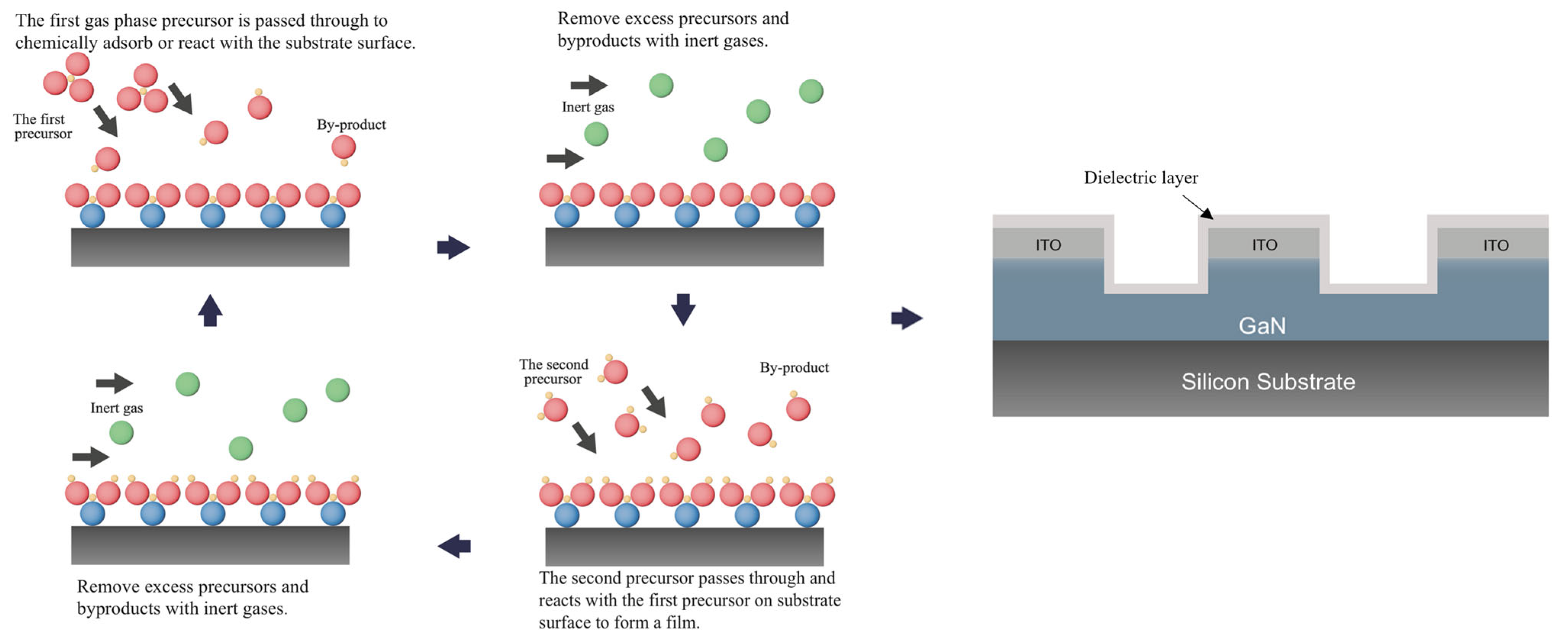
2.1. InGaN Epilayers and Schematic of the Device Process
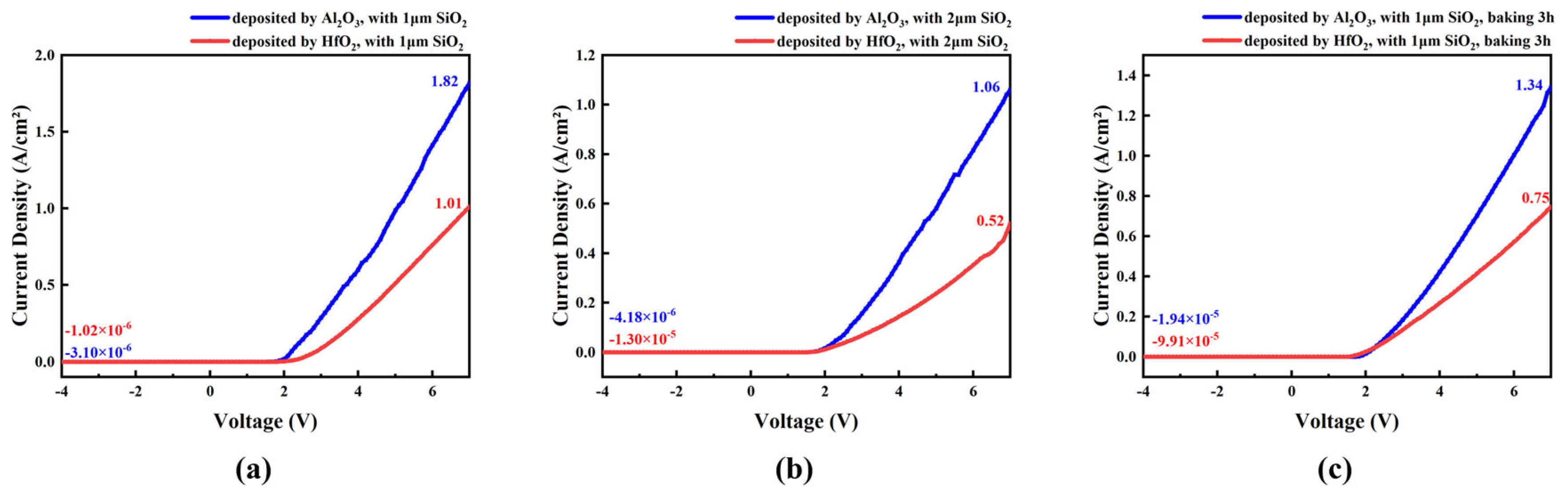
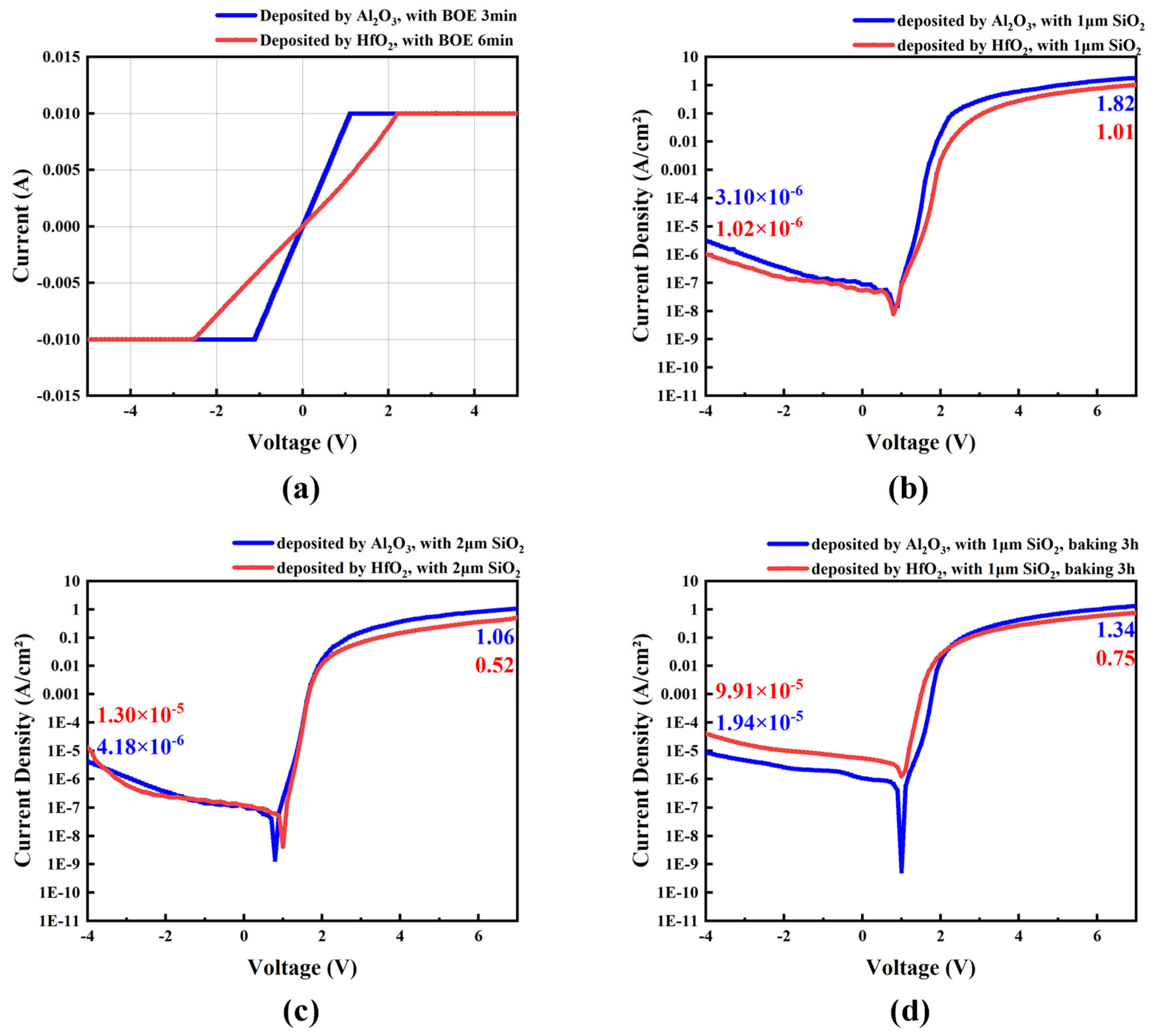
2.2. Dielectric Layer Passivation Treatment on Decreased Electrical Performance
3. Results
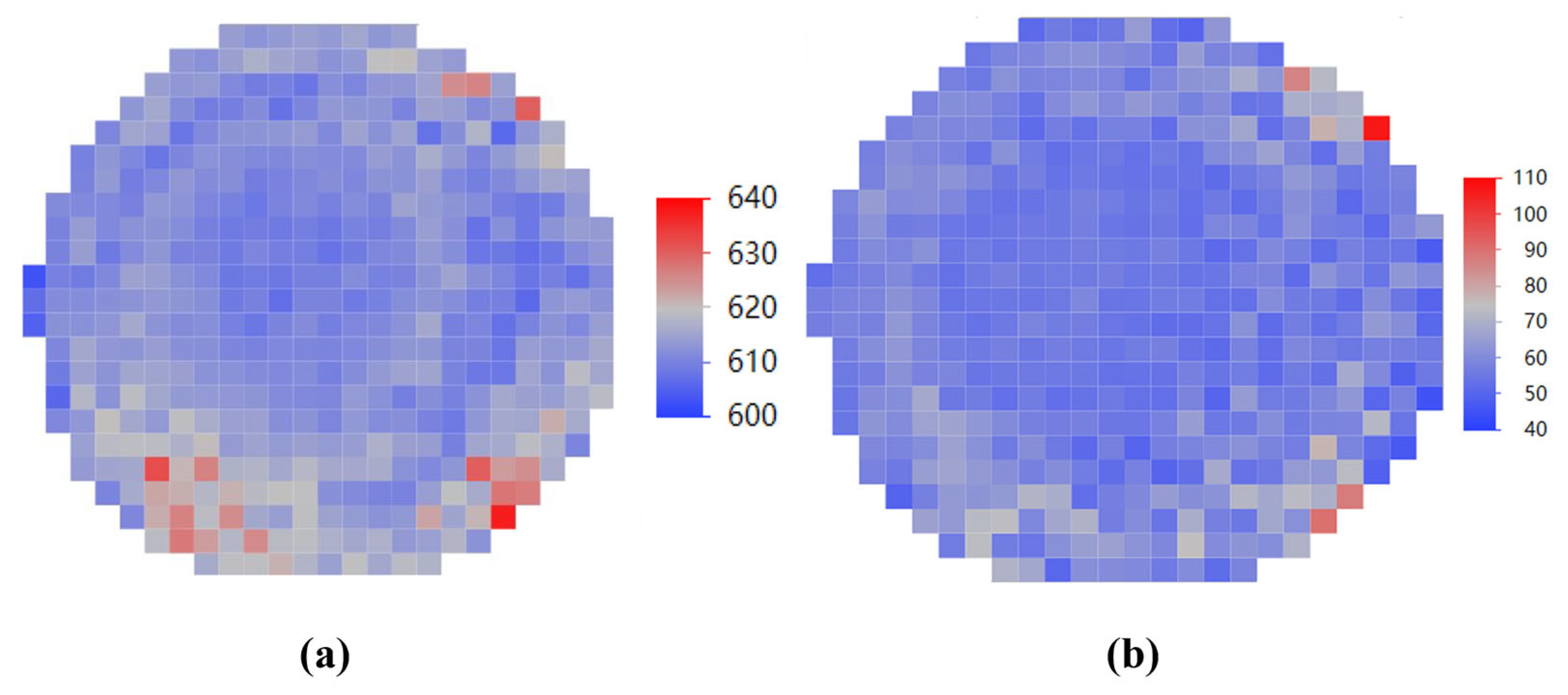
3.1. Characterization of Materials
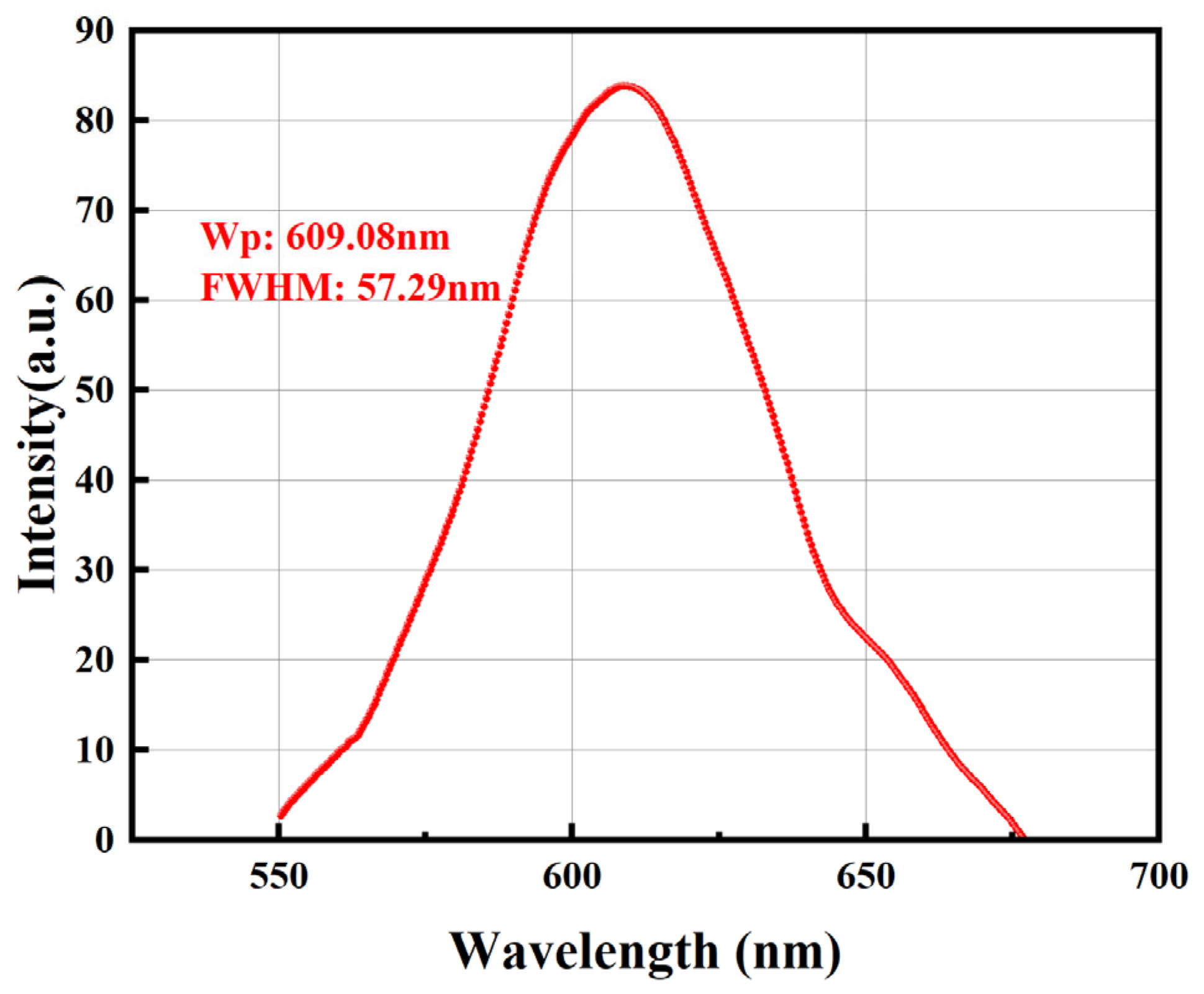
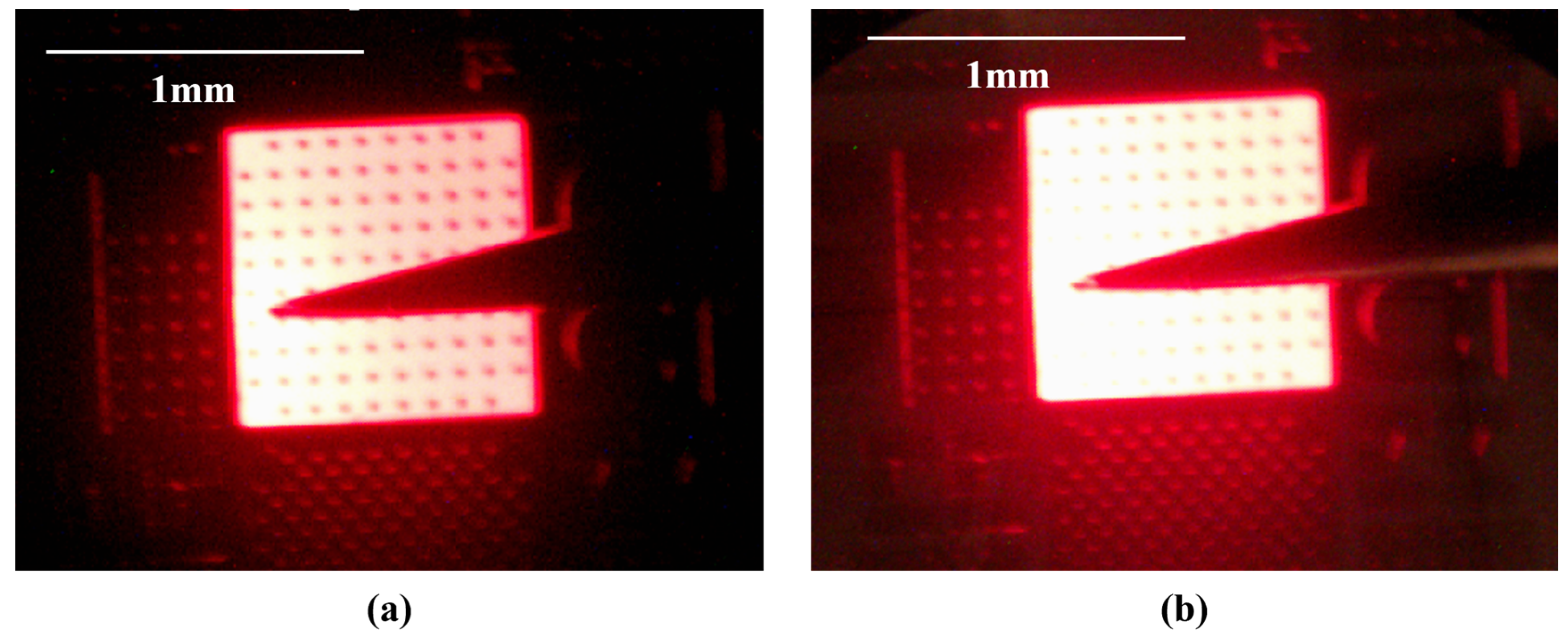
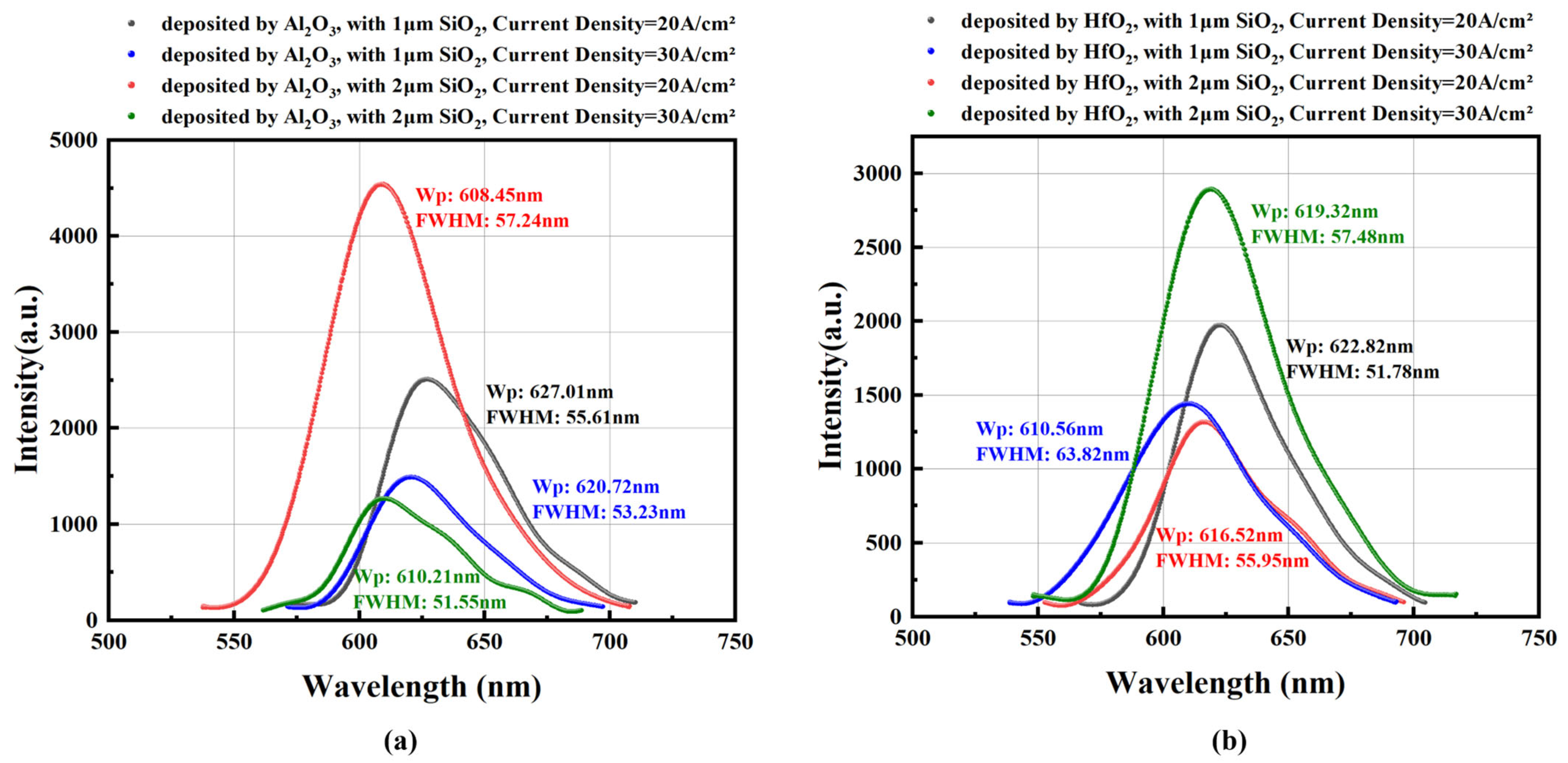
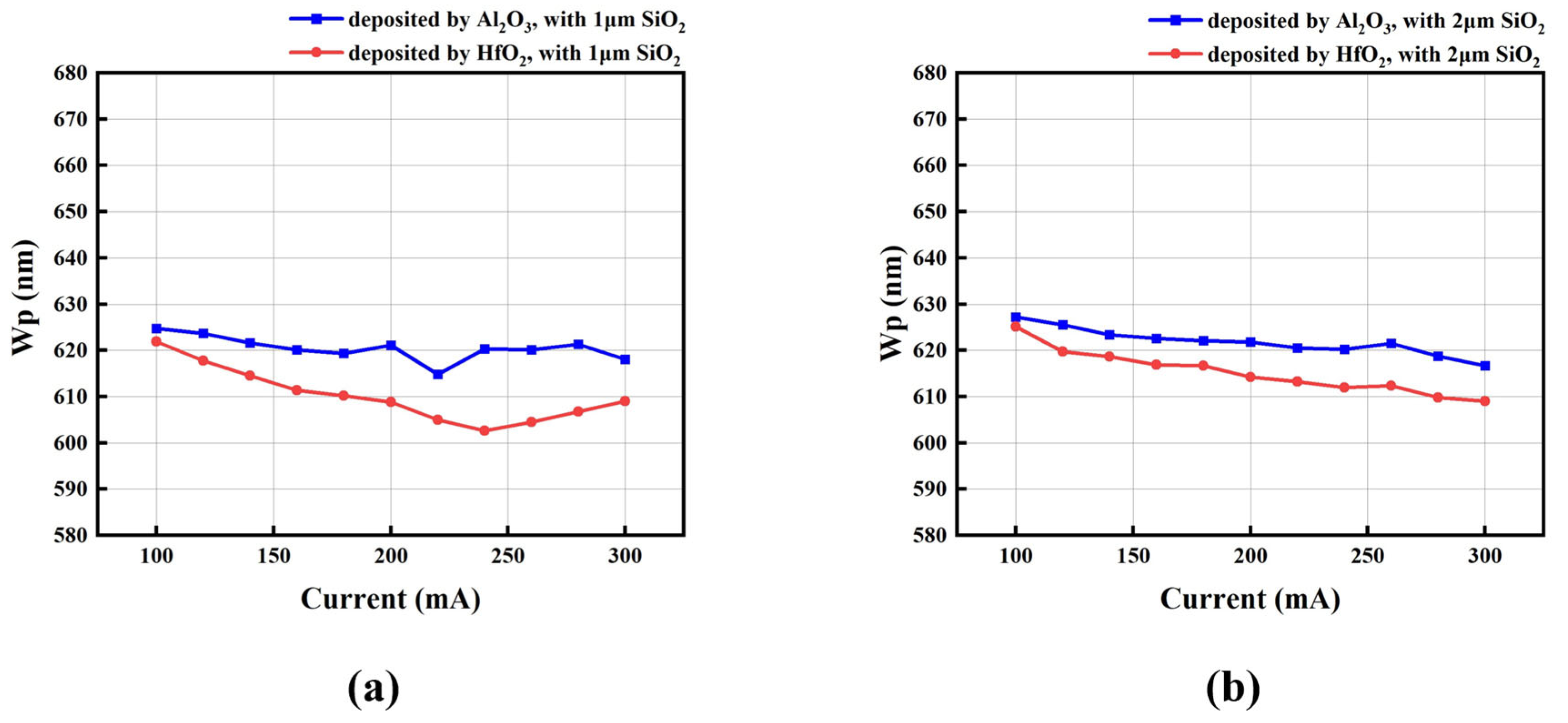
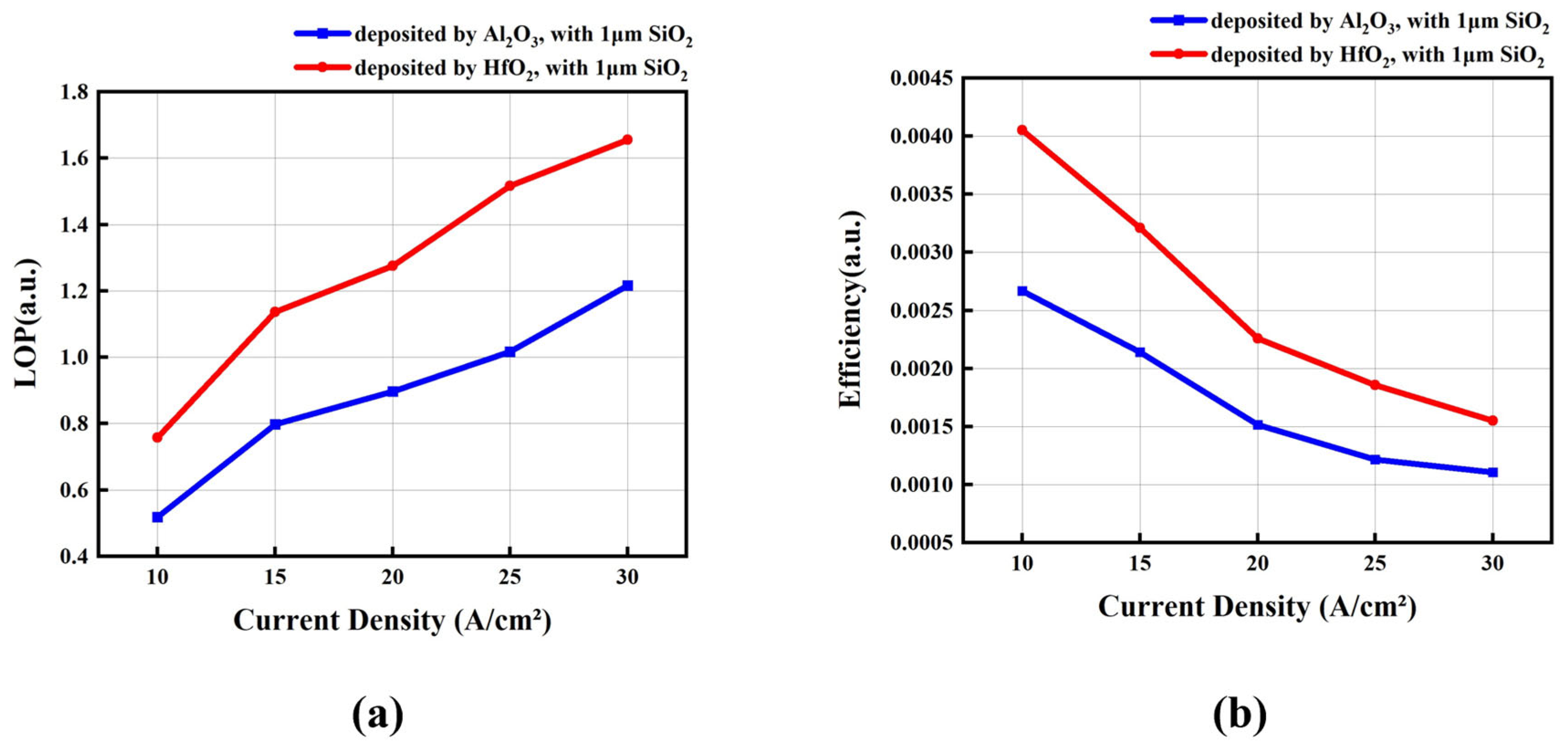
3.2. Optimized Electrical and Optical Performance
4. Conclusions
Author Contributions
Funding
Data Availability Statement
Acknowledgments
Conflicts of Interest
Appendix A
References
- Mishra, R.K.; Verma, K.; Chianella, I.; Goel, S.; Nezhad, H.Y. Nanomaterial integration in micro LED technology: Enhancing efficiency and applications. Next Nanotechnol. 2024, 5, 100056. [Google Scholar] [CrossRef]
- Liu, Y.; Wang, G.; Feng, F.; Zhanghu, M.; Yuan, Z.; Li, Z.; Xu, K.; Kwok, H.S.; Liu, Z. Ultra-low-defect homoepitaxial micro-LEDs with enhanced efficiency and monochromaticity for high-PPI AR/MR displays. PhotoniX 2024, 5, 23. [Google Scholar] [CrossRef]
- Joachim, P. Efficiency Models for GaN-Based Light-Emitting Diodes: Status and Challenges. Materials 2020, 13, 5174. [Google Scholar] [CrossRef]
- James Singh, K.; Huang, Y.-M.; Ahmed, T.; Liu, A.-C.; Huang Chen, S.-W.; Liou, F.-J.; Wu, T.; Lin, C.-C.; Chow, C.-W.; Lin, G.-R.; et al. Micro-LED as a Promising Candidate for High-Speed Visible Light Communication. Appl. Sci. 2020, 10, 7384. [Google Scholar] [CrossRef]
- Suryo, W.H.; Daniel, P.J.; Jan, G.; Andreas, W. Beyond solid-state lighting: Miniaturization, hybrid integration, and applications of GaN nano- and micro-LEDs. Appl. Phys. Rev. 2019, 6, 041315. [Google Scholar]
- Wonjae, C.; Jungsub, K.; Myoungsoo, K.; Woo, L.M.; Hyun, L.C.; Gunho, K.; Sunghyun, H.; Jeeyoung, C.; Hwan, M.Y.; Kiseong, J.; et al. Concurrent self-assembly of RGB microLEDs for next-generation displays. Nature 2023, 617, 287–291. [Google Scholar]
- Sfuncia, G.; Nicotra, G.; Giannazzo, F.; Pécz, B.; Gueorguiev, G.K.; Kakanakova-Georgieva, A. 2D graphitic-like gallium nitride and other structural selectivity in confinement at the graphene/SiC interface. CrystEngComm 2023, 25, 5810–5817. [Google Scholar] [CrossRef]
- Filho, M.A.M.; Farmer, W.; Hsiao, C.-L.; Dos Santos, R.B.; Hultman, L.; Birch, J.; Ankit, K.; Gueorguiev, G.K. Density functional theory-fed phase field model for semiconductor nanostructures: The case of self-induced core–shell InAlN nanorods. Cryst. Growth Des. 2024, 24, 4717–4727. [Google Scholar] [CrossRef]
- Daisuke, I.; Kazuhiro, O. Recent progress in red light-emitting diodes by III-nitride materials. Semicond. Sci. Technol. 2022, 37, 013001. [Google Scholar]
- Zhe, Z.; Daisuke, I.; Kazuhiro, O. InGaN-based red light-emitting diodes: From traditional to micro-LEDs. Jpn. J. Appl. Phys. 2022, 61, SA0809. [Google Scholar]
- Wu, H.; Lin, X.; Shuai, Q.; Zhu, Y.; Fu, Y.; Liao, X.; Wang, Y.; Wang, Y.; Cheng, C.; Liu, Y.; et al. Ultra-high brightness Micro-LEDs with wafer-scale uniform GaN-on-silicon epilayers. Light Sci. Appl. 2024, 13, 284. [Google Scholar] [CrossRef] [PubMed]
- Qi, L.; Zhang, X.; Chong, W.C.; Li, P.; Lau, K.M. 848 ppi high-brightness active-matrix micro-LED micro-display using GaN-on-Si epi-wafers towards mass production. Opt. Express 2021, 29, 10580–10591. [Google Scholar] [CrossRef] [PubMed]
- Yifan, W.; Jianshe, M.; Ping, S.; Lijun, Z.; Bizhong, X. Full-Color Realization of Micro-LED Displays. Nanomaterials 2020, 10, 2482. [Google Scholar] [CrossRef]
- Arifin, P.; Sugianto; Subagio, A.; Sutanto, H.; Dwiputra, D.; Florena, F.F.; Keintjem, A.C.; Khaeroni, R. Room-temperature photoluminescence of Mg-doped GaN thin films grown by plasma-assisted MOCVD. AIP Adv. 2020, 10, 045123. [Google Scholar] [CrossRef]
- Li, J.; Guo, Z.; Li, F.; Lin, H.; Li, C.; Xiang, S.; Zhou, T.; Wan, N.; Liu, Y. Performance enhancement of blue light-emitting diodes by using special designed n and p-type doped barriers. Superlattices Microstruct. 2015, 85, 454–460. [Google Scholar] [CrossRef]
- Jiang, Z.; Yan, D.; Zhang, N.; Wang, J.; Wei, X. Research on Evolution of Relevant Defects in Heavily Mg-Doped GaN by H Ion Implantation Followed by Thermal Annealing. Materials 2024, 1, 2518. [Google Scholar] [CrossRef]
- Surender, S.; Prabakaran, K.; Loganathan, R.; Pradeep, S.; Singh, S.; Baskar, K. Effect of growth temperature on InGaN/GaN heterostructures grown by MOCVD. J. Cryst. Growth 2016, 468, 249–251. [Google Scholar] [CrossRef]
- Sakurai, H.; Hideki, S.; Tetsuo, N.; Masato, O.; Shinji, Y.; Akihiko, K.; Malgorzata, I.; Keita, K.; Masahiro, H.; Nobuyuki, I.; et al. Redistribution of Mg and H atoms in Mg-implanted GaN through ultra-high-pressure annealing. Appl. Phys. Express 2020, 13, 086501. [Google Scholar] [CrossRef]
- Nakamura, S.; Iwasa, N.; Senoh, M.; Mukai, T. Hole Compensation Mechanism of P-Type GaN Films. Jpn. J. Appl. Phys. 1992, 31, 1258. [Google Scholar] [CrossRef]
- Shugurov, K.Y.; Mozharov, A.M.; Bolshakov, A.D.; Fedorov, V.V.; Mukhin, I.S. Hydrogen passivation of the n-GaN nanowire/p-Si heterointerface. Nanotechnology 2020, 31, 244003. [Google Scholar] [CrossRef]
- Nakamura, S.; Mukai, T.; Senoh, M.; Iwasa, N. Thermal Annealing Effects on P-Type Mg-Doped GaN Films. Jpn. J. Appl. Phys. 1992, 31, L139–L142. [Google Scholar] [CrossRef]
- Reshchikov, M.A.; Andrieiev, O.; Vorobiov, M.; Ye, D.; Demchenko, D.O.; McEwen, B.; Sandvik, S.S. Passivation of acceptors in GaN by hydrogen and their activation. Nanotechnology 2024, 36, 105704. [Google Scholar] [CrossRef] [PubMed]
- Okumura, H.; Martin, D.; Malinverni, M.; Grandjean, N. Backward diodes using heavily Mg-doped GaN growth by ammonia molecular-beam epitaxy. Appl. Phys. Lett. 2016, 108, 072102. [Google Scholar] [CrossRef]
- Cho, H.K.; Lee, J.Y.; Kim, C.S.; Yang, G.M. Influence of strain relaxation on structural and optical characteristics of InGaN/GaN multiple quantum wells with high indium composition. J. Appl. Phys. 2002, 91, 1166–1170. [Google Scholar] [CrossRef]
- Iida, D.; Kondo, Y.; Sowa, M.; Sugiyama, T.; Iwaya, M.; Takeuchi, T.; Kamiyama, S.; Akasaki, I. Analysis of strain relaxation process in GaInN/GaN heterostructure by in situ X-ray diffraction monitoring during metalorganic vapor-phase epitaxial growth. Phys. Status Solidi (RRL)-Rapid Res. Lett. 2013, 7, 211–214. [Google Scholar] [CrossRef]
- Yang, Y.; Cao, X.A. Removing plasma-induced sidewall damage in GaN-based light-emitting diodes by annealing and wet chemical treatments. J. Vac. Sci. Technol. B. Microelectron. Nanometer Struct. Process. Meas. Phenom. 2009, 27, 2337. [Google Scholar] [CrossRef]
- Tae-Yeon, S.; Hiroshi, A. Surface passivation of light emitting diodes: From nano-size to conventional mesa-etched devices. Surf. Interfaces 2020, 21, 100765. [Google Scholar]
- Kim, K.; Hua, M.; Liu, D.; Kim, J.; Chen, K.J.; Ma, Z. Efficiency enhancement of InGaN/GaN blue light-emitting diodes with top surface deposition of AlN/Al2O3. Nano Energy 2018, 43, 259–269. [Google Scholar] [CrossRef]
- Lee, D.H.; Lee, J.H.; Park, J.S.; Seong, T.Y.; Amano, H. Improving the Leakage Characteristics and Efficiency of GaN-based Micro-Light-Emitting Diode with Optimized Passivation. ECS J. Solid State Sci. Technol. 2020, 9, 055001. [Google Scholar] [CrossRef]
- Juhyuk, P.; Woojin, B.; Myeong, G.D.; Sanghyeon, K. Understanding the Sidewall Passivation Effects in AlGaInP/GaInP Micro-LED. Nanoscale Res. Lett. 2022, 17, 29. [Google Scholar]
- Wong, M.S.; Lee, C.; Myers, D.J.; Hwang, D.; Kearns, J.A.; Li, T.; Speck, J.S.; Nakamura, S.; DenBaars, S.P. Size-independent peak efficiency of III-nitride micro-light-emitting-diodes using chemical treatment and sidewall passivation. Appl. Phys. Express 2019, 12, 097004. [Google Scholar] [CrossRef]
- Nigro, R.L.; Schilirò, E.; Greco, G.; Fiorenza, P.; Roccaforte, F. Surface treatments on AlGaN/GaN heterostructures for gate dielectric Al2O3 thin films grown by Atomic Layer Deposition. Thin Solid Film. 2016, 617, 138–142. [Google Scholar] [CrossRef]
- Pradip, D.; Kosuke, Y.; Toshiharu, K.; Takashi, E.; Makoto, M. Bias-controlled photocurrent generation process in GaN-based ultraviolet p–i–n photodetectors fabricated with a thick Al2O3 passivation layer. Optik 2021, 245, 167691. [Google Scholar]
- Wong, M.S.; Hwang, D.; Alhassan, A.I.; Changmin, L.; Ryan, L.; Shuji, N.; DenBaars, S.P. High efficiency of III-nitride micro-light-emitting diodes by sidewall passivation using atomic layer deposition. Opt. express 2018, 26, 21324–21331. [Google Scholar] [CrossRef]
- Wang, T.; Zhang, X.; Liu, Y.; Chong, W.; Huang, Z.; Lu, Z.; Zhang, X.; Shi, W.; Wang, Q.; Zhang, B. GaN-on-Si micro resonant-cavity light-emitting diodes with dielectric and metal mirrors. Opt. Mater. 2023, 143, 114096. [Google Scholar] [CrossRef]
- Zhang, S.; Fan, Q.; Ni, X.; Tao, L.; Gu, X. Study on the Influence of KOH Wet Treatment on Red μLEDs. Crystals 2023, 13, 1611. [Google Scholar] [CrossRef]
- Liu, Y.; Feng, F.; Zhang, K.; Jiang, F.; Chan, K.W.; Kwok, H.S.; Liu, Z. Analysis of size dependence and the behavior under ultrahigh current density injection condition of GaN-based Micro-LEDs with pixel size down to 3 μm. J. Phys. D Appl. Phys. 2022, 55, 315107. [Google Scholar] [CrossRef]


| Group Number | Dielectric Layer | Thickness of SiO2 | Treatment |
|---|---|---|---|
| Control Group | Al2O3/30 nm | / | / |
| 1-1 | / | BOE for 3 min | |
| 1-2 | 1 μm | BOE for 8 min | |
| 1-3 | 2 μm | BOE for 15 min | |
| 1-4 | 1 μm | 350 °C Baking 3 h, BOE for 8 min | |
| Control Group | HfO2/30 nm | / | / |
| 2-1 | / | BOE for 6 min | |
| 2-2 | 1 μm | BOE for 11 min | |
| 2-3 | 2 μm | BOE for 18 min | |
| 2-4 | 1 μm | 350 °C Baking 3 h, BOE for 11 min |
Disclaimer/Publisher’s Note: The statements, opinions and data contained in all publications are solely those of the individual author(s) and contributor(s) and not of MDPI and/or the editor(s). MDPI and/or the editor(s) disclaim responsibility for any injury to people or property resulting from any ideas, methods, instructions or products referred to in the content. |
© 2025 by the authors. Licensee MDPI, Basel, Switzerland. This article is an open access article distributed under the terms and conditions of the Creative Commons Attribution (CC BY) license (https://creativecommons.org/licenses/by/4.0/).
Share and Cite
Qin, H.; Zhang, S.; Fan, Q.; Ni, X.; Tao, L.; Gu, X. Dielectric Passivation Treatment of InGaN MESA on Si Substrates for Red Micro-LED Application. Crystals 2025, 15, 267. https://doi.org/10.3390/cryst15030267
Qin H, Zhang S, Fan Q, Ni X, Tao L, Gu X. Dielectric Passivation Treatment of InGaN MESA on Si Substrates for Red Micro-LED Application. Crystals. 2025; 15(3):267. https://doi.org/10.3390/cryst15030267
Chicago/Turabian StyleQin, Hongyu, Shuhan Zhang, Qian Fan, Xianfeng Ni, Li Tao, and Xing Gu. 2025. "Dielectric Passivation Treatment of InGaN MESA on Si Substrates for Red Micro-LED Application" Crystals 15, no. 3: 267. https://doi.org/10.3390/cryst15030267
APA StyleQin, H., Zhang, S., Fan, Q., Ni, X., Tao, L., & Gu, X. (2025). Dielectric Passivation Treatment of InGaN MESA on Si Substrates for Red Micro-LED Application. Crystals, 15(3), 267. https://doi.org/10.3390/cryst15030267