Abstract
Two-dimensional (2D) materials with dangling-bond-free surfaces have attracted considerable attention in next-generation electronic applications due to their distinctive properties, such as high carrier mobility, short-channel immunity, and strong light-matter interactions. Recently, various methods have been developed for the preparation of 2D materials, including mechanical exfoliation, chemical vapor deposition, and chemical solution-based processes. Among these, solution processing provides a cost-effective and low-temperature approach for large-scale production. This review highlights recent advancements in solution-processed 2D materials, focusing on preparation methods and their applications in electronic and optoelectronic devices. Additionally, future perspectives are proposed to advance the breakthrough and commercialization of solution technologies for value-added chemical production.
1. Introduction
Two-dimensional (2D) nanomaterials have emerged as a revolutionary class of materials due to their exceptional mechanical, electrical, and optical properties. Since the discovery of graphene in 2004 [1], there has been extensive research on other layered 2D materials, including hexagonal boron nitride (h-BN) and transition metal dichalcogenides (TMDs) [2,3,4]. These materials have unique characteristics, including high surface areas, tunable bandgaps, mechanical flexibility, and enhanced charge transport properties, making them ideal for applications in nanoelectronics and optoelectronics [5,6,7]. Among the various synthesis methods for 2D materials, solution-based processing has attracted significant attention owing to its simplicity, scalability, and cost-effectiveness. Unlike mechanical exfoliation [8] and chemical vapor deposition (CVD) [9,10,11], solution processing enables the low-cost, large-scale, and low-temperature production of 2D material inks, which are suitable for deposition techniques like drop casting, inkjet printing, and spin coating [12,13,14]. This approach promotes the development of flexible and printed electronics, accelerating the commercialization of 2D materials.
However, the effectiveness of solution-processed 2D materials relies heavily on the ability to achieve high-quality exfoliation and dispersion while maintaining the intrinsic properties of the nanosheets [15]. Liquid-phase exfoliation (LPE) has been widely used to produce dispersions of 2D materials in liquid media by using ultrasonic energy to break the van der Waals (vdW) forces between the layers [16]. This method provides a straightforward way to obtain single-layer and few-layer flakes, but low yield, aggregation, and structural defects remain major challenges. Chemical and electrochemical intercalation techniques have also been explored o enhance the exfoliation efficiency, thereby allowing for better control over material thickness and lateral dimensions [17,18]. Similarly, wet chemical synthesis has been utilized to directly grow high-quality 2D materials from molecular precursors, enabling precise tuning of the composition, phase, and morphology [19].
Given the growing interest in solution-processed 2D materials, the present review focuses on recent advances in their synthesis, deposition, and application in device technologies. The author believes that this review can provide insights into the potential of solution-processed 2D materials for next-generation electronic and optoelectronic applications.
2. Various Strategies for Preparing 2D Material Inks
2.1. Liquid-Phase Exfoliation
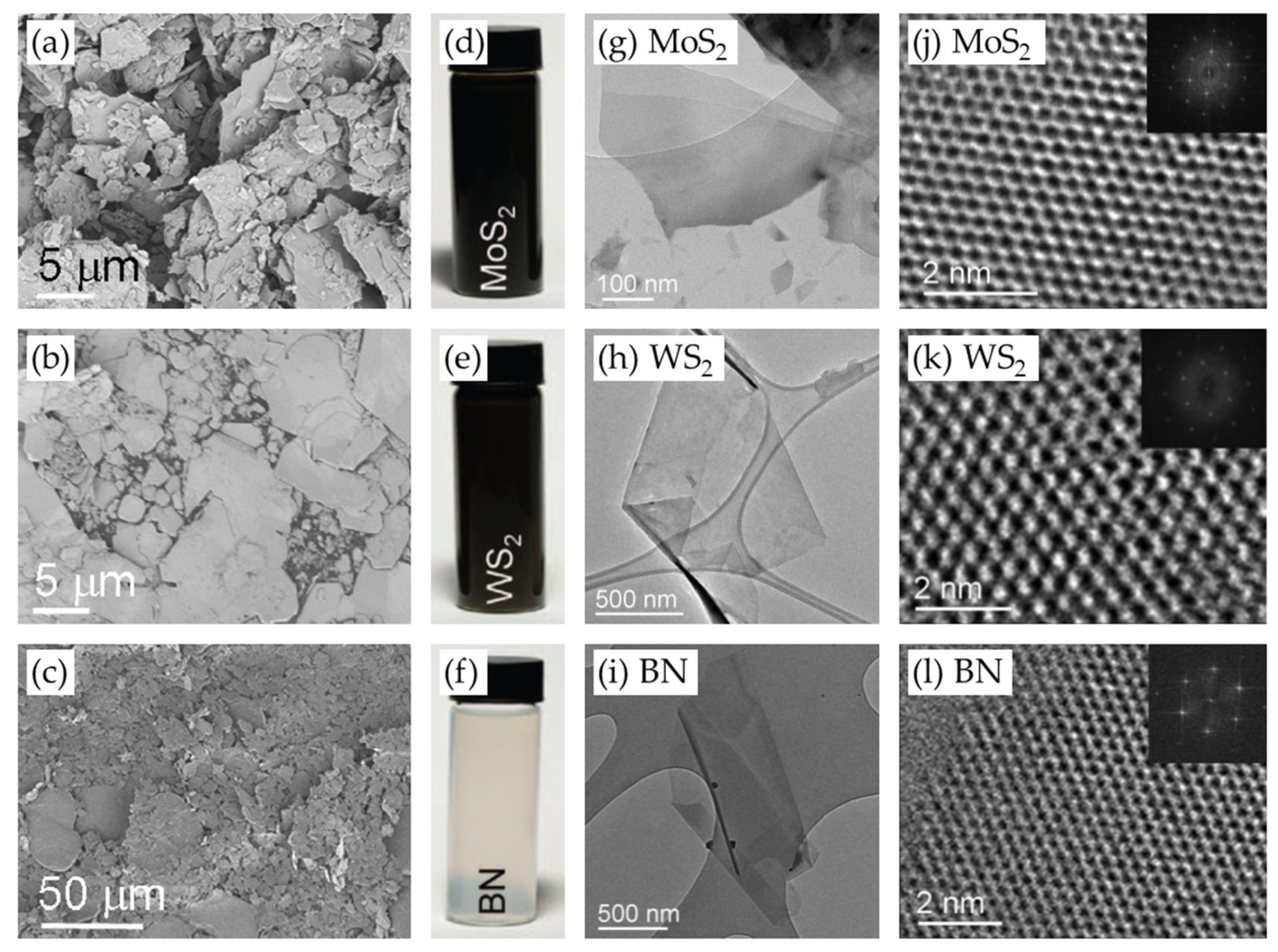
LPE is a common and simple method for the scalable production of high-quality 2D materials [16,20,21,22,23,24,25]. In contrast to the low yields of mechanical exfoliation and the complex growth conditions of CVD [26], LPE provides a simple, cost-effective, solution-based process for the isolation of monolayer and multilayer nanosheets. This method uses mechanical agitation in a solvent to break the van der Waals (vdW) forces between adjacent layers of materials like graphene, TMDs, and h-BN. The typical 2D materials prepared by LPE are shown in Figure 1 [16].
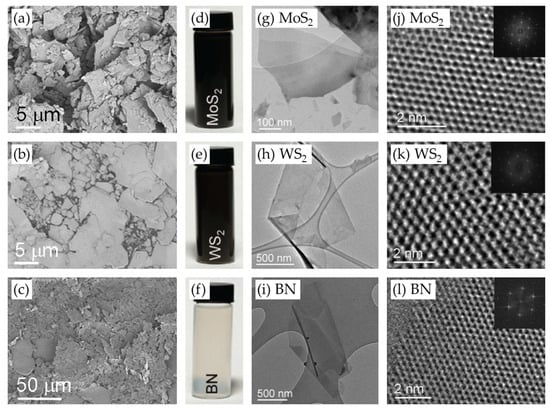
Figure 1.
(a–c) SEM images of 2D material powders, including (a) MoS2, (b) WS2, and (c) BN. (d–f) Photographic images of vials containing the corresponding 2D material dispersions obtained by sonication-assisted exfoliation. (g–i) Low-resolution TEM images of the corresponding liquid-phase exfoliated materials. (j–l) High-resolution TEM images of the corresponding monolayers, along with insets showing the corresponding fast Fourier transform (FFT) patterns. Reproduced with permission [16].
LPE involves the application of external energy, often in the form of ultrasonication or shear mixing, to delaminate bulk layered materials in liquid solvents. Therefore, the quality of the resultant 2D nanosheets is influenced by factors such as solvent selection, processing conditions, and the inherent properties of the target 2D materials [27,28,29,30,31]. Solvent selection is crucial for stabilizing the exfoliated nanosheets and preventing their re-aggregation. Common solvents such as N-methyl-2-pyrrolidone (NMP), dimethylformamide (DMF), and ortho-dichlorobenzene (o-DCB) closely match the surface energy of various 2D materials, ensuring dispersion stability [32,33]. However, these solvents often lead to environmental concerns due to their toxicity. Furthermore, their high boiling temperatures make them difficult to remove completely after exfoliation [20]. This residual solvent can lead to the degradation of device performance. Therefore, to mitigate the challenges associated with residual solvents, researchers have investigated aqueous dispersions stabilized by surfactants. Surfactants can be categorized into two types: ionic and non-ionic. Ionic surfactants include sodium cholate (SC) and sodium dodecyl sulfate (SDS), which provide electrostatic repulsion. On the other hand, non-ionic surfactants, such as Pluronic P-123, offer steric stabilization [34,35,36,37]. Recent advancements in LPE include the use of mixed solvents to optimize both the exfoliation efficiency and dispersion stability. Mixed-solvent systems can improve the overall process by combining a good solvent for insertion into the interlayers with a solvent that promotes dispersion. For instance, the combination of ethanol with dimethylacetamide can enhance the yield and minimize re-aggregation [38].
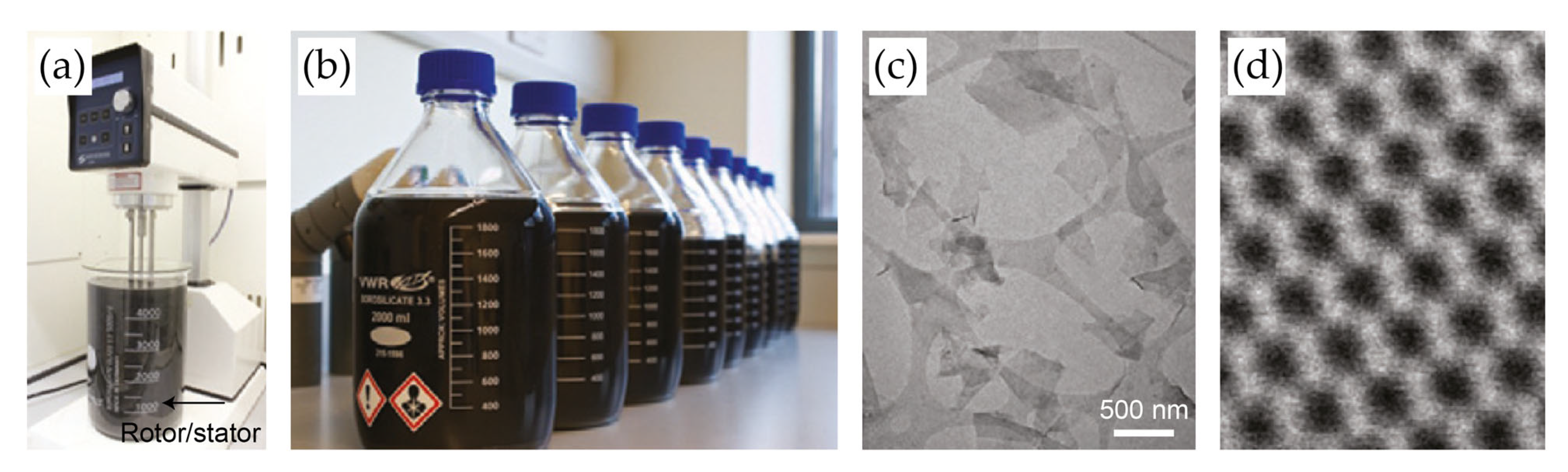
One of the most widely used LPE methods is ultrasonication. This process generates microscopic bubbles that break vdW forces between layers, thereby resulting in delamination. However, prolonged ultrasonication can fragment nanosheets, reducing their size and introducing defects [28,39]. Unlike sonication-based exfoliation, which often results in a broad size distribution, shear exfoliation provides better control over nanosheet dimensions while maintaining high yields [40,41,42,43,44]. For instance, Paton et al. demonstrated that the use of high-shear mixing to exfoliate bulk graphene in an aqueous surfactant solution enables large-scale production with tunable nanosheet sizes (Figure 2a,b) [41]. By varying the surfactant concentration and mixing parameters, Varrla et al. achieved MoS2 dispersions with lateral sizes ranging from 40 to 220 nm and thicknesses of 2–12 layers (Figure 2c) [45]. Meanwhile, Biccai et al. demonstrated that this technique is equally applicable to WS2 [40]. By optimizing the shear parameters, they achieved WS2 dispersions with a concentration of 1.82 g L−1, thereby surpassing the concentration of 0.77 g L−1 obtained through sonication-assisted exfoliation.

Figure 2.
(a,b) Photographic images of the shear mixer (a) and graphene dispersions (b) prepared by shear exfoliation methods. Shear mixing of graphite powder was conducted using an L5M high-shear laboratory mixer. Graphite was mixed with NMP and NaC solutions at speeds of 500–7000 r.p.m. for 3–540 min. The dispersion was then centrifuged to remove unexfoliated graphite. (c,d) Wide-field (c) and high-resolution (d) TEM images of exfoliated MoS2 nanosheets. Reproduced with permission [24].
2.2. Chemical Intercalation
The dispersion of exfoliated 2D nanosheets in liquid media has been frequently achieved via chemical intercalation [17]. This technique involves the insertion of small foreign species into the interlayer spaces of a vdW material to modify the interlayer distance and, hence, reduce the interlayer adhesion. To do this, a host material with a layered structure is immersed into a solution containing the intercalant atoms, ions, or molecules. The underlying mechanism of this process is primarily governed by redox reactions, where electron transfer occurs between the intercalant and the host material, or by electrostatic interactions, where the intercalants are attracted to the host material owing to opposite charges. Generally, the intercalant needs to be soluble in the chosen solvent, thereby allowing for uniform distribution throughout the solution [46]. Alternatively, the solvent itself can sometimes act as the intercalant by directly inserting itself into the interlayer spaces [47]. In addition, the host material must maintain chemical stability in the solvent, which should not react with the host material, thereby preserving its characteristics during the intercalation process. For instance, Koski et al. introduced a chemical method for inserting zero-valent metals such as Ag, Au, Co, Cu, Fe, In, Ni, and Sn into a layered Bi2Se3 [48]. This specific method is distinguished by the fact that the intercalation of metal atoms into the host structure does not induce a change in the oxidation or valence state of the host material. Other layered crystals, such as MoO3, Sb2Te3, In2Se3, and GaSe, have also been successfully used as host materials for this type of intercalation [49,50]. Meanwhile, Liu et al. demonstrated a novel spontaneous self-intercalation mechanism whereby copper (Cu) atoms are intercalated into the vdW gaps of Group IV and V TMDs at room temperature and atmospheric pressure [51]. First-principles density functional theory (DFT) calculations revealed that the Gibbs free energy (ΔG) for Cu intercalation is negative for group IV and V TMDs, thereby indicating a spontaneous and thermodynamically favorable self-intercalation process. However, for group VI TMDs such as MoS2 and WS2, ΔG is positive, which means that Cu atoms do not intercalate naturally into these materials.
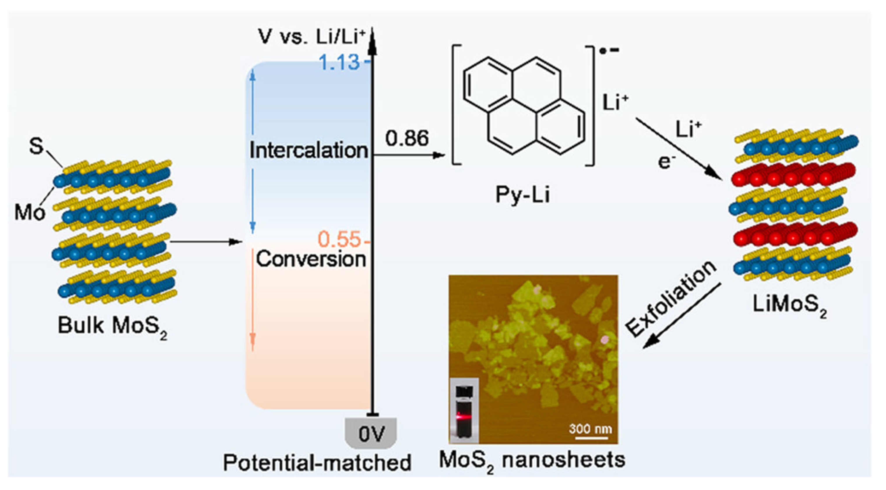
Beyond zero-valent metal intercalation, metal ions such as Li+, Na+, and K+ can penetrate layered materials [52,53,54]. For instance, Ambrosi et al. reported a chemical lithiation method utilizing n-butyllithium (n-BuLi) to intercalate lithium directly into MoS2 in a hexane solution at 100 °C [52]. Meanwhile, Zheng et al. utilized the pyrophoric properties of n-BuLi to develop a novel sodium naphthalenide-based exfoliation process [55]. In this approach, bulk MoS2 was treated with hydrazine (N2H4) under hydrothermal conditions, thus leading to pre-expansion of the layered structure. The resulting expanded MoS2 powder was then dipped into a sodium naphthalenide (Na+C10H8−) solution formed by reacting sodium metal with naphthalene in anhydrous tetrahydrofuran (THF). Finally, MoS2 nanosheets were exfoliated to monolayers in water under mild sonication. This method offers a high yield of monolayer flakes with lateral dimensions exceeding 10 µm, which significantly surpasses previous n-BuLi exfoliation methods [56,57]. However, N2H4 generates explosive gases such as H2 and NH3. To overcome this safety issue, Zhu et al. used pyrene lithium (Py-Li) as an intercalant (Figure 3) [18]. The well-matched redox potential of Py-Li led to complete lithium insertion at room temperature, thereby significantly reducing the processing time while maintaining a monolayer yield of 80%.
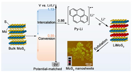
Figure 3.
Schematic illustrations of the pristine bulk MoS2 (left), the redox potential of Py-Li and intercalation and decomposition potentials of bulk MoS2 (middle left), the molecular structure of Py-Li (middle right, top), the lithium-intercalated MoS2 (right), along with an AFM image (middle right, bottom) of the exfoliated MoS2 nanosheets. Reproduced with permission [18].
Gamble et al. presented the insertion of charge-neutral molecules such as ammonia, pyridine, aniline, and tributylphosphine into the interlayer spaces of niobium disulfide and tantalum disulfide [58]. Meanwhile, Feng et al. developed a polymer-directed intercalation strategy in which polyethyleneimine (PEI) and polyethylene glycol (PEG) molecules were directly intercalated into MoS2 at room temperature [59]. Furthermore, the process resulted in the formation of MoS2-polymer composites that, upon carbonization, yielded MoS2/carbon heteroaerogels. The resulting materials exhibited an interlayer expansion of 0.98 nm and a high MoS2 concentration of 74%. In another study, Jeong et al. developed a novel tandem molecular intercalation (TMI) approach for exfoliating 2D materials [60]. This method uses two intercalates, including short “initiator” molecules that widen the interlayer gap, and longer “primary” molecules that fully expand the gap, thereby enabling spontaneous exfoliation into single layers. By using appropriate intercalants, single-layer TMDs such as TiS2, ZrS2, NbS2, WSe2, and MoS2 have been successfully produced.
2.3. Electrochemical Intercalation
As shown in Figure 4, electrochemical intercalation applies an external electrochemical potential to insert charged species into layered materials [61]. The electrochemical process typically takes place within a specially designed test cell, where the host material acts as either the cathode or anode, depending on the charge of the intercalating species [62,63,64,65]. The extent of intercalation is primarily governed by the applied electrochemical potential (voltage); however, the current density also influences the intercalation kinetics [66,67,68].

Figure 4.
(a,b) Schematic diagrams showing (a) the electrochemical intercalation of MoS2 crystals and (b) the intercalation, exfoliation, and deposition of the bulk MoS2. (c) Photographic images of MoS2 before and after intercalation (scale bars = 5 mm). (d) A schematic illustration of the pristine MoS2 (left) and the expanded MoS2 crystal (right) after intercalation. Reproduced with permission [61].
When the layered material serves as the anode, the intercalating species must carry a negative charge, and the intercalation process is driven by the application of a positive voltage to the 2D material [69,70]. However, a positive voltage can also induce oxidation of the host material. Such oxidation reactions are often undesirable, as they can alter the chemical composition and structural integrity of the materials [71]. By contrast, cathodic intercalation involves the application of a negative potential to the electrochemical cell, thereby minimizing oxidation-related issues. This method is widely used for lithium-ion battery cathodes, where Li+ ions intercalate into layered materials such as graphite and TMDs [53]. During the discharge cycle, Li+ ions migrate into the cathode material, thus facilitating energy storage. Electrochemical intercalation is not limited to inorganic ions; it also enables organic molecule intercalation. For example, Wan et al. introduced a method of synthesizing n-type inorganic/organic superlattices by intercalating organic molecules into layered TiS2 [72]. This superlattice synthesis involved a two-step chemical process: electrochemical intercalation followed by solvent exchange.
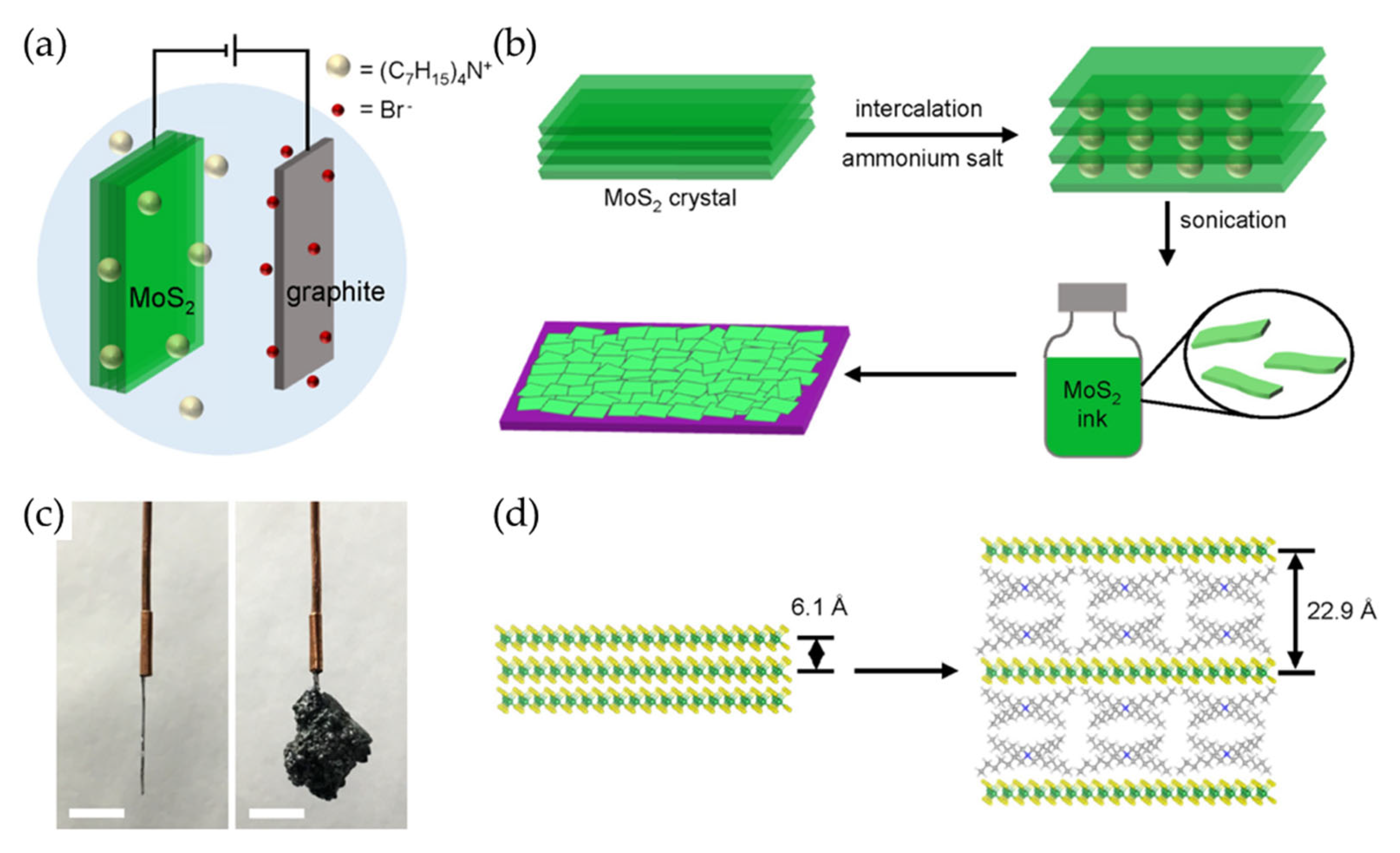
The recent literature has provided a broad library of 2D material inks prepared by liquid-metal-assisted electrochemical intercalation that allows direct exfoliation of crystal powders without high-temperature processing or polymer additives (Figure 5) [73]. This approach uses a conductive and adhesive liquid metal such as Galinstan to facilitate the intercalation of organic cations into the layered crystal powders. The liquid metal serves as a flexible medium that accommodates volume expansion during intercalation while maintaining strong electrical contact with the microcrystals. This liquid-metal-assisted method has successfully expanded the range of solution-processable 2D materials, enabling the exfoliation of more than 50 different types of layered crystals. These include TMDs such as ZrS2, NbSe2, and MoTe2; main-group metal chalcogenides such as InSe, SnSe2, and Bi2Se3; ternary layered compounds such as MnPS3 and ZnIn2S4; layered oxides such as MoO3 and V2O5; and elemental materials such as graphene and phosphorene. Notably, this method has also enabled the exfoliation of wide-bandgap 2D semiconductors, including GaS and GaSe.
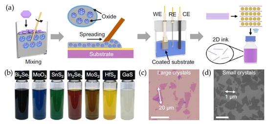
Figure 5.
(a) A schematic illustration of the liquid-metal-assisted electrochemical intercalation of 2D materials. A uniform suspension was prepared by dispersing 2D crystal powders into liquid Galinstan consisting of gallium, indium, and tin. The suspension was then spread onto a substrate, which served as the working electrode. The electrochemical intercalation process was then applied to expand the 2D crystals. Finally, 2D monolayers were obtained through ultrasonication. (b) Photographic images of various exfoliated 2D nanosheets dispersed in DMF. (c,d) Optical (c) and SEM (d) images of exfoliated MoS2 nanosheets deposited on a SiO2/Si substrate. Reproduced with permission [73].
Recently, He et al. demonstrated an electrochemical molecular intercalation and exfoliation method to obtain high-purity InSe monolayers while minimizing oxidation [74]. The process was carried out in a nitrogen-filled glovebox to eliminate exposure to oxygen and moisture, which can degrade InSe. In this method, the bulk InSe crystals served as the cathode in an electrochemical cell, while a conductive graphite rod acted as the anode. A solution of tetraheptylammonium bromide (THAB) in acetonitrile was used as the electrolyte. During intercalation, a voltage of −3.2 V was applied for 2 h to facilitate the insertion of organic cations between the InSe layers, thereby causing the bulk crystal to expand. After intercalation, the material was transferred to DMF and subjected to mild bath sonication for exfoliation, thereby resulting in monolayer InSe nanosheets.
2.4. Wet Chemical Synthesis
Wet chemical methods have emerged as potential candidates for the scalable production of 2D materials. By carefully manipulating reaction parameters such as precursor concentration, temperature, and reaction duration, researchers have successfully synthesized high-quality monolayer and few-layer 2D materials. For example, Jung et al. proposed a method for producing WSe2 and MoSe2 in liquid media by using tungsten hexacarbonyl (W(CO)6) and molybdenum hexacarbonyl (Mo(CO)6) as tungsten and molybdenum precursors, respectively [75]. The study demonstrated that modulating the binding affinities of capping ligands enables precise control over the nanosheet thickness. In this work, MoCl5, oleic acid (OA), oleylamine, and TDPA solution were degassed overnight, after which CS2 was added. This precursor solution was slowly injected into oleylamine, while maintaining the temperature at 320 °C, to result in the formation of MoS2 nanosheets. Single-layer WSe2 nanosheets were similarly obtained by using OA as the ligand, whereas oleyl alcohol and oleylamine resulted in multilayer growth due to their stronger binding at the edges. Meanwhile, the wafer-scale colloidal synthesis of few-layer MoS2 nanosheets was realized by Son et al. via a hot-injection method in which the precursor solution was slowly injected into hot oleylamine (Figure 6) [76]. This method allows synthesis at lower temperatures than CVD and enables large-scale production, yielding 2.19 g of MoS2. Furthermore, the as-synthesized nanosheets showed superior size and thickness uniformity compared to exfoliated MoS2.
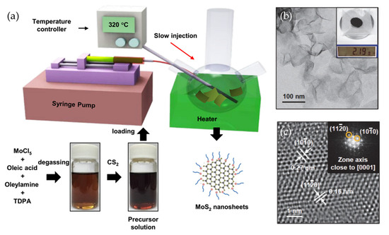
Figure 6.
(a) A schematic illustration of MoS2 nanosheet preparation via wet chemical synthesis. To synthesize MoS2 nanosheets, MoCl5 and TDPA were dissolved in degassed oleic acid and oleylamine. CS2 was then injected into the precursor solution, and the mixture was slowly introduced into oleylamine using a syringe pump. After aging, trioctylphosphine was added to remove excess sulfur. (b) A low-resolution TEM image of the as-synthesized MoS2 nanosheets, along with an inset showing the obtained mass. (c) A high-resolution TEM image of the MoS2 nanosheets, along with an inset showing the corresponding FFT analysis. Reproduced with permission [76].
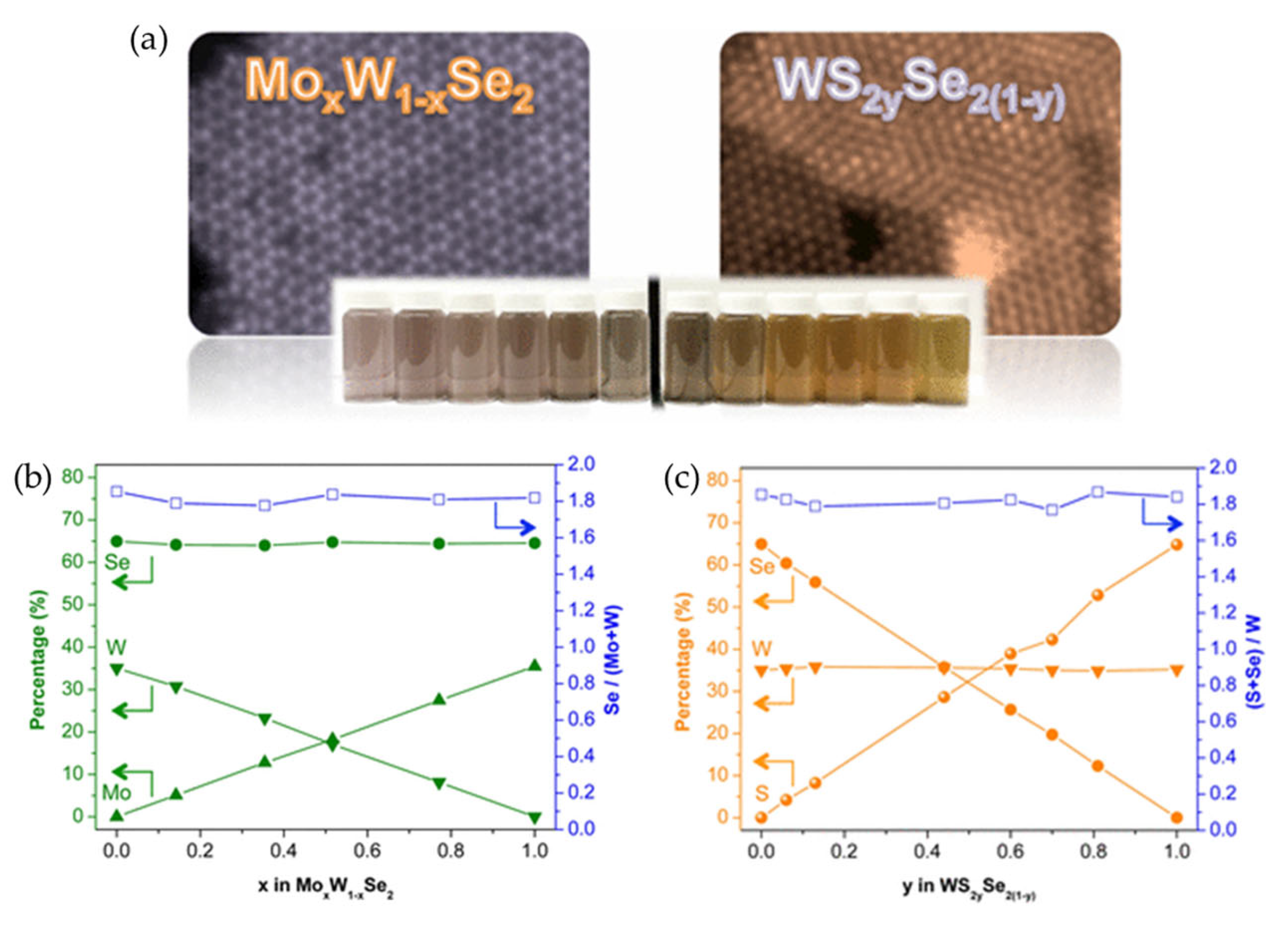
Barrera et al. demonstrated a versatile solution-based route for synthesizing few-layer 2D MX2 TMD flakes (where M = Mo, W and X = S, Se) via the microwave-assisted thermolysis of organometallic precursors [19]. A key aspect of this synthesis was the use of 1,2-hexadecanediol (HDD) as a reducing agent. The HDD concentration was found to be critical for achieving a high M4+ content corresponding to the MX2 stoichiometry, and for suppressing the formation of unwanted metal oxides. A low-temperature solution synthesis was reported for MoxW1−xSe2 and WS2xSe2(1−x), which enabled full control of the metal and chalcogen composition [77]. Moreover, the resulting colloidal TMD alloys exhibited continuously tunable optical properties, with excitonic transitions ranging from 1.51 to 1.93 eV.
Meanwhile, Sun et al. synthesized few-layer 1T’-MoTe2 in a solution phase by gradually injecting a MoCl5-OA solution into a hot mixture of trioctylphosphine (TOP), trioctylphosphine telluride (TOP-Te), oleylamine, and hexamethyldisilazane (HMDS) at 300 °C [78]. The study suggested that MoCl5 likely reacts with OA during the synthesis to form molybdenum oleate, while oleylamine provides a reducing atmosphere, thus facilitating MoTe2 formation. The HMDS was found to be essential for producing crystalline MoTe2 nanostructures with high yield and uniformity. In another study, Martín García et al. designed a colloidal synthesis of ReS2 using rhenium pentachloride (ReCl5) and elemental sulfur as precursors, thereby avoiding hazardous sulfur sources such as CS2 or dodecanethiol (DDT) [76,79,80]. The reaction involved dropwise injection of a ReCl5-OA solution into a hot oleylamine–sulfur solution at 350 °C under an argon atmosphere. The resultant nanosheets exhibited a lateral domain size of ~4 nm and a thickness of around 0.4 nm, which was slightly lower than that of mechanically exfoliated ReS2 monolayers. This size reduction was attributed to strain effects in these highly anisotropic colloidal structures. Meanwhile, Wang et al. demonstrated a solution-phase synthesis route for the production of large-area tellurene (Te) nanosheets [81]. This process involved reducing sodium tellurite (Na2TeO3) with N2H4 in an alkaline solution at 160–200 °C in the presence of polyvinylpyrrolidone (PVP). The PVP was used to control the size, shape, and thickness, thereby enabling the formation of tellurene flakes with lateral dimensions of up to 100 μm and tunable thicknesses ranging from monolayers to tens of nanometers. Precise control over the Te thickness was achieved by adjusting the Na2TeO3/PVP ratio. Lower PVP concentrations tended to accelerate nucleation, thus resulting in smaller crystals, while higher PVP contents supported the formation of larger flakes. The optimal Na2TeO3/PVP ratio for obtaining minimal thickness was found to be 52.4:1 (group 12 in Figure 7c). The productivity was found to increase with the increase in temperature up to 180 °C but tended to saturate at 200 °C due to potential bond disruption between Te chains.
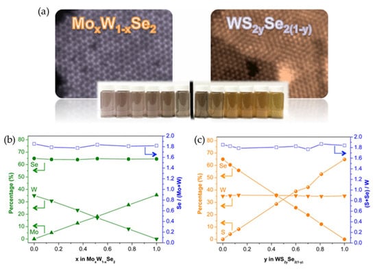
Figure 7.
(a) Atomically resolved ADF-STEM images of MoxW1−xSe2 (top left) and WS2xSe2(1−x) (top right). Photographic images of TMD alloys dispersed in ethanol (bottom). Photographs show the composition-dependent optical properties of colloidal TMD alloys. (b,c) Plots of the relative amounts of Mo, W, S, and Se in the MoxW1−xSe2 (b) and WS2xSe2(1−x) (c) alloy nanostructures. Reproduced with permission [77].
The key features, advantages, and limitations of solution-processing methods for 2D materials are summarized in Table 1.

Table 1.
Comparison of solution-processing techniques for 2D materials.
3. Electronic and Optoelectronic Applications
3.1. Thin-Film Transistors
Traditional thin-film transistor (TFT) fabrication relies on expensive and high-temperature processing techniques such as CVD and molecular beam epitaxy (MBE). By contrast, solution processing enables the scalable production of 2D material-based TFTs at low temperatures. The fabrication of solution-processed 2D TFTs typically involves several steps. First, the 2D material is exfoliated and an ink is prepared. This can be achieved via liquid-phase exfoliation, electrochemical intercalation, or wet chemical synthesis to disperse the nanosheets in a suitable solvent, thereby creating a stable ink. The ink is then deposited onto a substrate using methods such as spin-coating, drop casting, or Langmuir–Blodgett deposition, followed by controlled drying to form a uniform thin film. For instance, Zeng et al. constructed a MoS2 ink by using an LPE method and used it to fabricate a TFT [82]. In that study, a two-step exfoliation process involving NMP and isopropanol (IPA) produced well-dispersed MoS2 flakes, which were then used to fabricate bottom-gate TFTs via spray coating. When subsequently coated with a PMMA layer to improve the charge transfer between flakes, the as-fabricated TFTs exhibited enhanced electrical performance. Electrical characterization revealed nonlinear current-voltage (I-V) behavior, which was attributed to back-to-back Schottky barriers at the inter-flake connections. In the assembled MoS2 TFTs, a low carrier mobility of 10−4 cm2 V−1 s−1 was demonstrated. Meanwhile, Xi et al. demonstrated a selective solution-based synthesis method for fabricating MoS2 TFTs by enabling the direct growth of MoS2 on the gold (Au) electrodes and TFT channel region, with the Au electrodes serving as both electrical contacts and catalytic surfaces [83]. For deposition, a 0.014 M MoS2 precursor solution was prepared and mixed with hydrazine hydrate. The substrate with pre-patterned Au electrodes was immersed in the solution, heated to 90 °C for 27 min, and subsequently cleaned, dried, and annealed at 350 °C under a N2 atmosphere. The resulting MoS2 film exhibited a thickness of 73 nm on Au and gradually thinned to 11 nm in the channel. The as-fabricated MoS2 TFT exhibited an on/off ratio of 106 and a carrier mobility of 0.4 cm2 V−1 s−1 with typical n-type behavior.
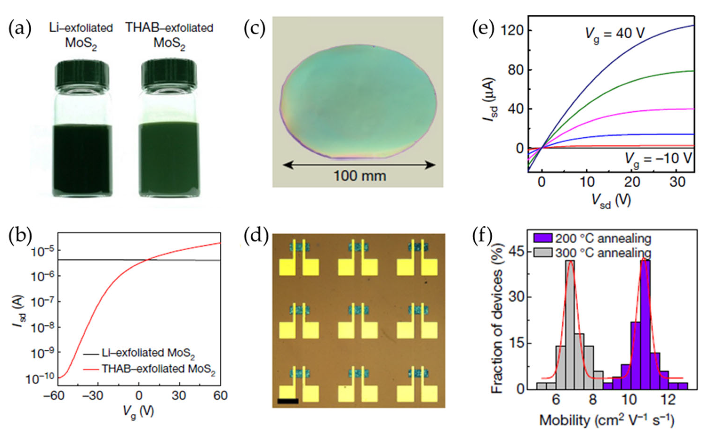
Lithium intercalation-assisted exfoliation is a typical solution-based method that often results in the formation of metallic 1T-phase MoS2, which exhibits poor electrical performance in TFTs due to a high off-state current [84,85]. Additionally, liquid-phase exfoliation techniques frequently lead to a broad distribution of nanosheet thicknesses, which cause non-uniform charge transport properties. These limitations hinder the practical implementation of 2D semiconductor nanosheets in TFTs and other electronic applications. To address these challenges, a novel approach based on electrochemical intercalation using quaternary ammonium molecules was developed by Lin et al. (Figure 8) [86]. This method enabled the production of highly uniform, phase-pure semiconducting nanosheets with well-defined thickness distributions. Specifically, by intercalating large organic cations such as THAB into layered MoS2 crystals, the extent of electron injection was effectively controlled, thereby preventing the undesirable phase transition to the metallic state. The expanded MoS2 layers were then subjected to mild sonication to facilitate exfoliation into semiconducting 2H-MoS2 nanosheets with a narrow thickness distribution. The resultant MoS2 nanosheets exhibited exceptional electrical properties when incorporated into TFTs. Compared to Li-exfoliated MoS2 films, which typically exhibit low field-effect mobilities of 0.1 cm2 V−1 s−1, the devices fabricated using THAB as an intercalant achieved mobilities of approximately 10 cm2 V−1 s−1 and on/off current ratios of 106. Furthermore, the process was extended to the exfoliation of other 2D materials, including WSe2, Bi2Se3, NbSe2, In2Se3, Sb2Te3, and black phosphorus.

Figure 8.
(a) Photographic images of Li- and THAB-intercalated MoS2 ink solutions. (b) The measured transfer curves of field-effect transistors (FETs) consisting of the Li- and THAB-exfoliated MoS2. (c) A photographic image of the MoS2 thin film deposited on a 100 mm SiO2/Si substrate. (d) An optical micrograph of a MoS2 TFT array (scale bar = 100 μm). (e) The output characteristics of large-area MoS2 TFTs with various gate voltages. (f) A histogram of the mobility for the solution-processed MoS2 TFTs after post-annealing at 200 and 300 °C. Reproduced with permission [87].
Yan et al. demonstrated thin films based on solution-processed 2D materials on the surfaces of plant leaves or human skin [88]. These freestanding films were designed to provide exceptional mechanical stretchability, thereby allowing them to seamlessly integrate with biological tissues while maintaining electronic properties. Unlike thin films produced by CVD, which often contain polycrystalline domains with covalently bonded grain boundaries, these thin films rely on weak vdW interactions between nanosheets. The weak vdW interfaces in these 2D materials allow nanosheets to slide and rotate among the staggered nanosheets, giving the films excellent flexibility, stretchability, and conformability. The abovementioned researchers therefore fabricated electronic devices such as leaf-gate transistors and skin-gate transistors using these vdW thin films as active layers.
While n-type 2D materials such as MoS2 have shown superior electronic performance, the development of analogous high-performance p-type materials via solution processing has remained a substantial challenge. In this respect, black phosphorus exhibits excellent hole transport characteristics but suffers from poor stability due to oxidation [89]. On the other hand, chemically stable p-type TMDs such as WSe2 typically show low hole mobilities, thus making them unsuitable for high-performance applications. Additionally, solution-processing techniques often lead to nanosheet aggregation, high inter-flake resistance, and poor charge injection at metal contacts due to Fermi-level pinning, which further limits the efficiency of p-type 2D transistors [90]. Nevertheless, Zou et al. reported a significant enhancement in the hole mobility of solution-processed p-type WSe2 transistors via molecular doping with bromine (Br2) [91]. The field-effect mobility of the Br2-doped WSe2 transistors exceeded 27 cm2 V−1 s−1, which was orders of magnitude higher than that of the undoped devices. Furthermore, these transistors exhibited high on/off current ratios (~107) and excellent operational stability under switching cycles and bias stress conditions.
In addition to semiconducting channels, metallic and insulating 2D materials can also be fabricated by solution processing. For example, Kim et al. demonstrated an all-solution-based process for the fabrication of 2D material field-effect transistors (FETs) by integrating various electronic building blocks, such as metallic graphene, semiconducting MoS2, and insulating hafnium oxide (HfO2) [70]. The resulting all-solution processed MoS2 FETs exhibited field-effect mobilities of 8.3 cm2 V−1 s−1 and on/off current ratios exceeding 106.
3.2. Non-Volatile Memory Electronics
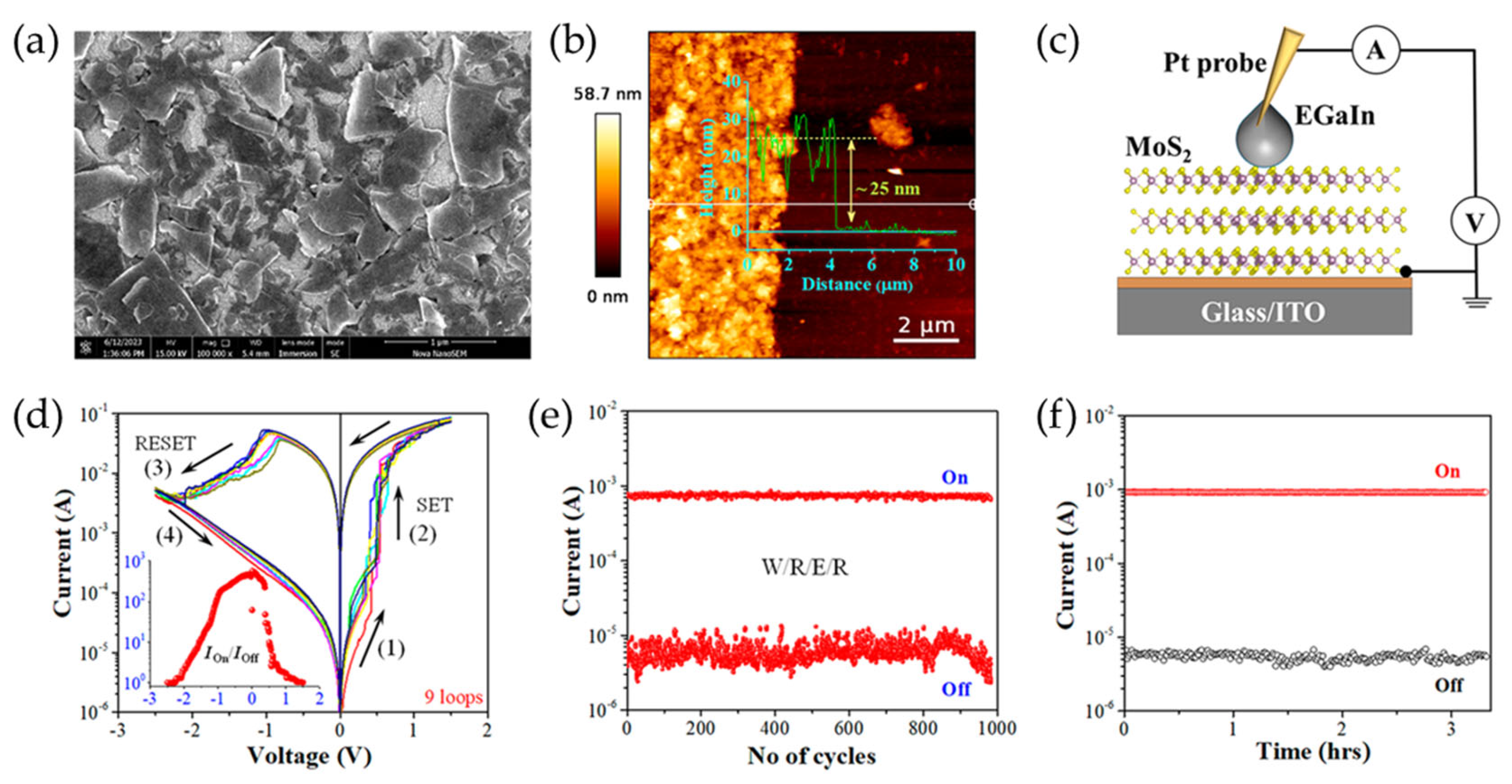
In addition to TFTs, non-volatile memory (NVM) devices are essential components of modern computing architectures, enabling long-term data storage with minimal power consumption. Traditional NVM technologies such as flash memory and dynamic random-access memory (DRAM) face limitations related to scalability, endurance, and power efficiency. Hence, solution-processed 2D materials have emerged as promising candidates for next-generation NVMs due to advantages such as thickness tunability and compatibility with flexible substrates. Recent progress in solution-processed resistive random-access memory (RRAM) and memristors based on MoS2, WSe2, and h-BN has demonstrated excellent endurance, fast switching speeds, and low-power operation. These developments are paving the way for advancements in neuromorphic computing, in-memory computing, and monolithic 3D memory integration. Solution-processed 2D NVM devices typically comprise a metal-insulator-metal (MIM) structure, where the active layer, often a TMD or h-BN, is sandwiched between two electrodes. An applied voltage induces a transition between high and low resistance states due to mechanisms such as charge trapping or ionic migration. Saha et al. demonstrated that solution-processed MoS2 thin films offer a scalable approach for the fabrication of memristors with non-volatile resistive switching behavior (Figure 9) [92]. In that study, a biphasic method was used to deposit defect-free MoS2 thin films, thereby ensuring uniform nanosheet stacking and strong interlayer interactions. This method involved the LPE of MoS2 nanosheets in NMP, followed by transfer to IPA for the formation of an interfacial layer between two immiscible liquids. The memristor, made of solution-processed MoS2 thin films between indium tin oxide (ITO) and eutectic gallium indium (EGaIn) electrodes, exhibited an on/off current ratio of about 103, a high endurance of at least 103 cycles, and a data retention exceeding 104 s. The switching mechanism was attributed to charge carrier trapping and detrapping at sulfur vacancy sites within the MoS2 nanosheets.
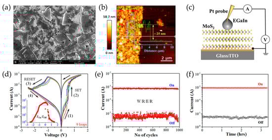
Figure 9.
(a,b) SEM (a) and AFM (b) images of solution-processed MoS2 thin films. (c) A schematic illustration of an EGaIn/MoS2/ITO memristor. (d) Representative I-V curves for various MoS2 memristors. The different colored lines represent the multiple voltage loops obtained by repeating the bias sweeps. The inset shows the Ion/Ioff ratio as a function of applied voltage. (e,f) The endurance (e) and retention (f) characteristics of the device in the high resistance state (HRS) and low resistance state (LRS). Reproduced with permission [92].
To integrate 2D materials into large-scale circuits, Tang et al. fabricated memristor arrays at the wafer scale using solution-processed MoS2 thin films [93]. These devices demonstrated forming-free resistive switching behavior characterized by a high endurance of over 107 cycles, along with low device-to-device variability and excellent retention times of more than 10 years. Furthermore, the potential of solution-processed MoS2 memristors in neuromorphic computing was demonstrated through the successful implementation of a convolutional neural network (CNN) model for pattern recognition. With excellent linear conductance updates and low variability, the MoS2 memristor array achieved a high recognition accuracy of 98.02% for handwritten Modified National Institute of Standards (MNIST) digits.
Recently, Liu et al. exploited the quantum-confined Stark effect to control the conduction properties of solution-processed MoS2 [94]. According to their study, combining MoS2 with a ferroelectric polymer such as poly(vinylidene fluoride-trifluoroethylene) (P(VDF-TrFE)) results in a substantial nonlinear conduction switching effect, with an on/off ratio exceeding 105. Using density functional theory (DFT) calculations and in situ spectroscopy, the authors explained this modulation by the bandgap narrowing under a localized electric field. This bandgap narrowing causes a considerable increase in the concentration of free carriers, thus leading to improved electrical conductivity while maintaining carrier mobility. The authors also reported that this conduction modulation strategy could be applied to other solution-processed 2D materials, such as molybdenum ditelluride and bismuth telluride.
3.3. Optoelectronic Applications
Photodetectors are essential components in optoelectronics, enabling applications in imaging, optical communication, and environmental sensing. However, while traditional silicon-based photodetectors are widely used, they encounter challenges related to scalability, flexibility, and cost-effective production. Solution-processed 2D materials like MoS2, MoSe2, WSe2, and black phosphorus offer high optical absorption, tunable bandgaps, and mechanical flexibility, making them promising candidates for next-generation photodetectors [95]. Recent advancements in solution-processing techniques have enabled the fabrication of highly sensitive, flexible, and transparent photodetectors with superior responsivity and fast response times.
In 2013, Cunningham et al. prepared solution-processed MoS2 films exhibiting photoconductive behavior [96]. To fabricate the MoS2 photodetectors, the bulk MoS2 crystals were first exfoliated via solvent-based sonication, after which the MoS2 nanosheets were deposited via the Langmuir–Blodgett technique. Thus, a dispersion of MoS2 nanosheets was carefully deposited onto the surface of the water, where they spread to form a continuous layer due to their hydrophobic nature [97]. The substrate (e.g., ITO-coated glass) was then submerged beneath the water surface and slowly withdrawn at a controlled angle, allowing the MoS2 nanosheets to adhere to the substrate. Multiple dipping cycles were used to increase the film thickness. After deposition, the films were annealed at moderate temperatures to improve the crystallinity and reduce any residual solvent effects. The ITO/MoS2/Au structure initially exhibited low dark conductivity, which increased about fourfold when exposed to light at an intensity of 1 kW/m2 due to the photoexcited charge carriers.
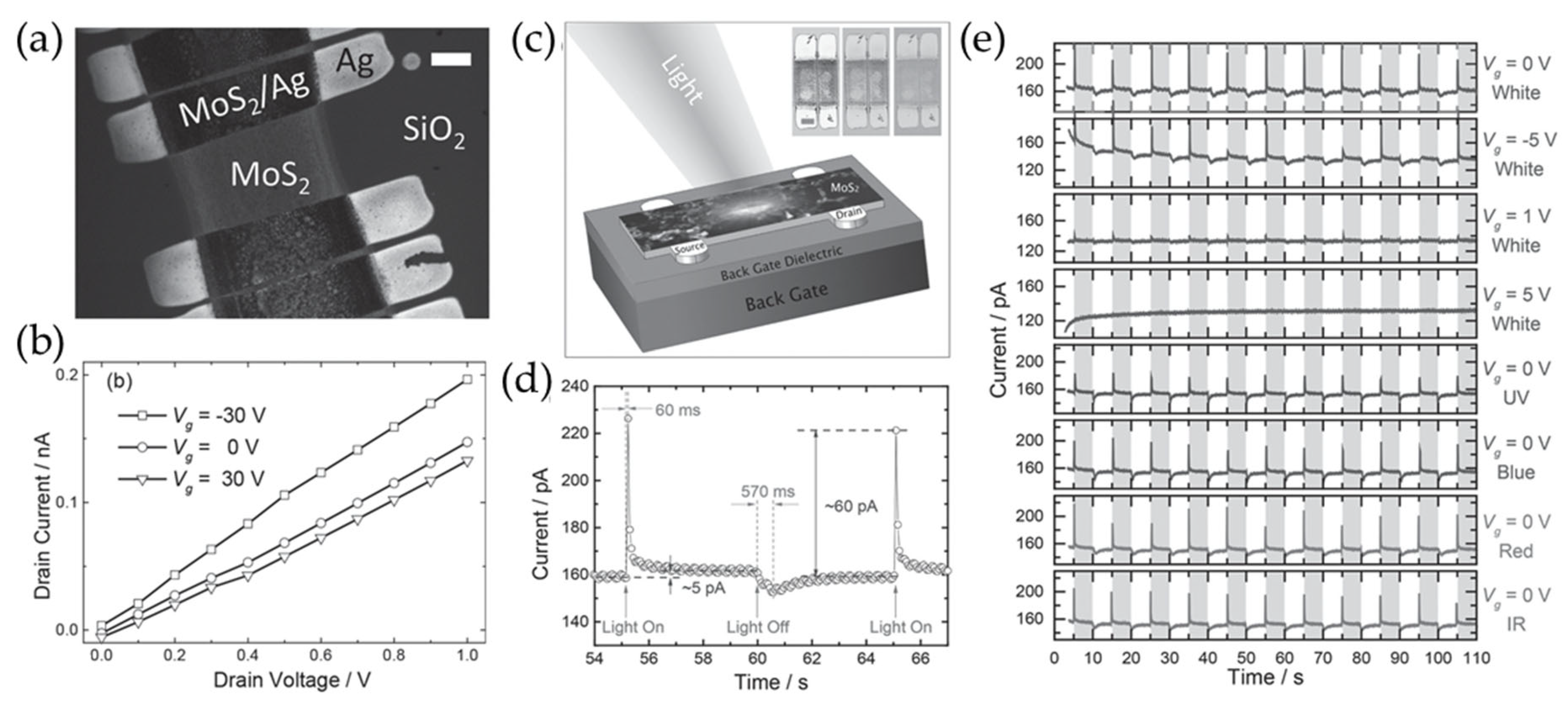
Meanwhile, Li et al. used inkjet printing technology to ensure the solution-processed deposition of MoS2 patterns with high resolution (Figure 10) [98]. In particular, polymer stabilizers such as ethyl cellulose (EC) were introduced to prevent nanosheet aggregation and improve ink uniformity. This polymer also acted as a surfactant, thereby enabling better adhesion of the printed patterns onto various substrates. Additionally, solvent exchange techniques were used to overcome the high volatility and toxicity of common organic solvents such as DMF and NMP. By using a Dimatix DMP 2800 inkjet printer, well-defined MoS2 patterns were deposited onto silicon dioxide (SiO2)/silicon (Si) substrates. The printing resolution was about 80 µm, and the printed patterns showed high uniformity. The printed MoS2 photodetectors exhibited fast rise and decay times of about 60 and 570 ms, respectively, similar to monolayer MoS2 photodetectors made with the mechanical exfoliation method [99,100].
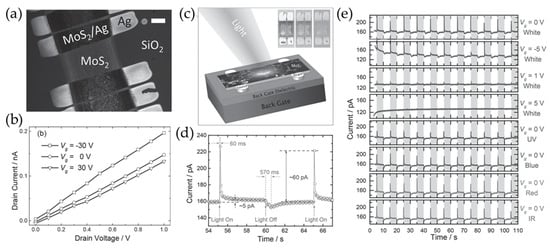
Figure 10.
(a) An SEM image of inkjet printed devices consisting of MoS2 and Ag as a channel and electrode (scale bar = 100 μm). (b) The output curves of the fabricated devices at various gate voltages. (c) A schematic representation of the printed MoS2 photodetectors. (d) The time-dependent photocurrent of the device, measured under white light with an intensity of 0.35 mW/mm2. (e) The time-resolved photocurrent under various gate bias and illumination conditions. Reproduced with permission [98].
MoS2 has a tunable bandgap, strong light absorption, and excellent photoconductivity. Graphene, with high carrier mobility, exhibits efficient charge transport behavior. Consequently, heterostructures consisting of MoS2 and graphene provide improved charge transport and enhanced photoresponsivity [101,102]. For instance, Liu et al. developed printable and transfer-free MoS2/graphene heterostructures by using MoS2 ink [103]. Owing to the absence of a graphene transfer process, a clean interface between the MoS2 and graphene was implemented, thereby facilitating efficient charge movement. The transfer-free MoS2/graphene photodetectors showed rise and decay times of 20 and 30 ms, respectively. These values are an order of magnitude faster than those of previously reported MoS2/graphene devices fabricated using transferred graphene, with response times ranging from 0.28 to 1.5 s [104,105].
The integration of solution-processed 2D materials onto flexible substrates has opened up new possibilities for low-cost, scalable device applications, particularly in photodetection [106,107]. For instance, Lobo et al. presented a novel approach utilizing MoS2 nanosheets deposited on paper substrates to fabricate flexible, high-performance photodetectors [25]. The photodetectors were fabricated by spray-coating liquid-phase exfoliated MoS2 dispersions onto screen-printed carbon electrodes on the paper substrates. The resulting devices maintained a robust photoresponse even under mechanical flexure, demonstrating the viability of this approach for flexible electronics. Electrical characterization revealed that calendaring, a compression process using rollers, significantly improved the device performance by decreasing the inter-nanosheet junction resistances and enhancing the charge transport pathways. As a result, the electrical conductivity was increased by six orders of magnitude, thus leading to photodetectors with responsivities of up to 6 mA/W.
In addition to MoS2, layered indium selenide (InSe) has emerged as a promising material for high-performance optoelectronic devices due to its unique optical structure and direct bandgap in multilayers. For example, Kang et al. exfoliated InSe in a cosolvent system composed of ethanol and water to eliminate residual surface contamination and chemical degradation [108]. The liquid-phase exfoliated InSe nanosheets exhibited high photoresponsivity of 5 × 10⁷ A W−1, which is superior to that of mechanically exfoliated InSe flakes [109]. Furthermore, thin-film devices fabricated using this approach showed ultrafast rise and decay times of 450 and 90 μs, respectively. Meanwhile, Li et al. demonstrated all-solution processed flexible photodetectors composed of InSe and Cu as the channel and electrode, respectively (Figure 11) [110]. To fabricate such a structure, Cu electrodes were prepared by photolithography-patterning polymer-assisted metal deposition (pp-PAMD). Flexible InSe photodetectors were then fabricated by spin-coating InSe nanoflake suspensions onto these Cu electrodes. The as-fabricated photodetectors exhibited high stability under diverse conditions, including 5000 on/off laser cycles, 20 weeks of ambient storage without encapsulation, thermal variation from 90 to 360 K, and 5000 bending cycles at a 2 mm radius.
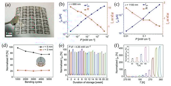
Figure 11.
(a) A photographic image of a flexible PET substrate with pp-PAMD_Cu electrodes. (b,c) The photocurrent and responsivity values of the device as a function of incident power at excitation wavelengths of (b) 690 nm and (c) 1100 nm. (d,e) The mechanical stability (d) and durability (e) of the InSe photodetectors. The different colored lines in (e) represent the normalized Iph of the device stored for different durations. (f) The dependence of the photocurrent on temperature for the InSe photodetectors. The different colored lines represent the normalized Iph of the device measured at different temperatures. Reproduced with permission [110].
Beyond single-layer TMDs as the active layer, Yadav et al. presented an approach for fabricating ultrathin 2D tri-layer heterostructures based on TMDs, specifically MoS2/MoSe2/TiS2, for photodetector applications [111]. The tri-layer heterostructure was synthesized using a liquid-phase exfoliation technique, followed by vacuum filtration to deposit the nanosheets layer by layer onto a membrane substrate. Photodetection measurements conducted at 660 and 785 nm revealed responsivity values of approximately 28 and 44 mA/W, respectively. The response times of the devices were found to be 220 and 250 ms at 660 and 785 nm, respectively. These results suggest that the heterostructure effectively reduces electron-hole recombination and enhances charge carrier separation, thus leading to improved photodetection performance.
Table 2 presents the performance metrics of devices based on solution-processed 2D materials.
Table 2.
Performance of devices employing solution-processed 2D materials as channel layers.
4. Conclusions and Perspectives
Solution-processed two-dimensional (2D) materials offer a promising route for developing scalable and cost-effective electronic and optoelectronic devices. Advances in liquid-phase exfoliation, chemical intercalation, electrochemical exfoliation, and wet chemical synthesis have enabled the production of high-quality 2D nanosheets that are suitable for large-area applications. Various deposition techniques, including spray coating, inkjet printing, and self-assembly, have further triggered the integration of these materials into functional devices such as TFTs, memories, photodetectors, and flexible electronics. Despite the recent progress, solution-processed 2D materials still face critical limitations hindering their integration into practical devices.
From an industrialization perspective, the scalable production of two-dimensional (2D) material-based films is crucial for commercialization. Such large-scale production not only reduces fabrication costs but also enhances process productivity. However, a critical obstacle to scalability is the difficulty in maintaining uniformity in the morphology of the exfoliated flakes produced during exfoliation. Flakes with small lateral dimensions or excessive thickness inhibit the uniformity of device performance. This leads to unnecessary material waste and ultimately lowers the production yield. To address this, precise control over the solution-phase exfoliation and stabilization processes is essential. In particular, optimizing the choice and concentration of solvents or surfactants mitigates nanosheet re-aggregation, preserving their thin, large-area morphology throughout exfoliation and deposition.
Besides scalability, the issue of long-term stability must be addressed. Many solution-processed 2D materials suffer from rapid degradation when exposed to ambient conditions, which significantly impact device lifetime and reliability. Encapsulation and surface passivation strategies can mitigate degradation. Engineering intrinsic material stability through defect passivation and healing also offers a promising pathway to enhance durability. Solution processing often causes uncontrolled defect formation, such as sulfur or selenium vacancies. These defects can trap charge carriers, reduce mobility, and introduce variability in device performance. Therefore, controlling defects in solution-processed 2D materials is vital for consistent device fabrication. To minimize defects in solution-processed 2D materials, several approaches can be employed. One effective strategy involves optimization of the exfoliation and dispersion parameters, such as solvent polarity, sonication power, and exfoliation time, to reduce structural damage during processing. Additionally, exposure to chalcogen precursors (e.g., sulfur or selenium vapor) can passivate dangling bonds and fill anion vacancies. Furthermore, introducing mild reductants or defect-healing agents into the solution during processing can suppress defect formation at early stages, thereby improving the electric and optoelectronic properties of the resulting nanosheets.
In addition, poor physical contact between the 2D flakes disrupts charge transfer pathways, thereby degrading overall device performance. This poor interfacial compatibility results in increased inter-flake resistance, restricting the potential of solution-processed 2D materials in electronic and optoelectronic applications. To overcome these limitations, strategies, including post-deposition annealing and the use of conductive binders or cross-linkers to enhance flake-to-flake connectivity, can be employed. These approaches promote stronger interfacial interactions and reduce the energy barriers at nanosheet junctions, ultimately improving charge transport across the flakes.
Finally, environmental factors are critical to advancing solution processing methods. However, the widespread use of toxic solvents, such as NMP and DMF, creates significant barriers to eco-friendly and industrial-scale applications. Therefore, optimizing process parameters to minimize solvent use and waste generation is essential. This can be achieved through techniques such as solvent recycling. In addition, alternative exfoliation methods, using non-toxic solvents, such as aqueous solution, provide sustainable and safe pathways for solution-processed 2D material-based devices. With continued advancements in scalable synthesis and device integration, solution-processed 2D materials hold significant potential for commercial applications, particularly in flexible electronics, optoelectronics, and next-generation computing technologies.
Funding
This work was supported by a National Research Foundation (NRF) of Korea grant, funded by the Korean government (MSIT) (2021R1C1C2094189).
Data Availability Statement
No new data were created or analyzed in this study.
Conflicts of Interest
The author declares no conflicts of interest.
References
- Novoselov, K.S.; Geim, A.K.; Morozov, S.V.; Jiang, D.; Zhang, Y.; Dubonos, S.V.; Grigorieva, I.V.; Firsov, A.A. Electric field effect in atomically thin carbon films. Science 2004, 306, 666–669. [Google Scholar] [PubMed]
- Kim, K.S.; Kwon, J.; Ryu, H.; Kim, C.; Kim, H.; Lee, E.-K.; Lee, D.; Seo, S.; Han, N.M.; Suh, J.M.; et al. The future of two-dimensional semiconductors beyond Moore’s law. Nat. Nanotechnol. 2024, 19, 895–906. [Google Scholar] [PubMed]
- Zeng, S.; Liu, C.; Zhou, P. Transistor engineering based on 2D materials in the post-silicon era. Nat. Rev. Electr. Eng. 2024, 1, 335–348. [Google Scholar]
- Cao, W.; Bu, H.; Vinet, M.; Cao, M.; Takagi, S.; Hwang, S.; Ghani, T.; Banerjee, K. The future transistors. Nature 2023, 620, 501–515. [Google Scholar]
- Chhowalla, M.; Jena, D.; Zhang, H. Two-dimensional semiconductors for transistors. Nat. Rev. Mater. 2016, 1, 16052. [Google Scholar]
- Wang, S.; Liu, X.; Xu, M.; Liu, L.; Yang, D.; Zhou, P. Two-dimensional devices and integration towards the silicon lines. Nat. Mater. 2022, 21, 1225–1239. [Google Scholar]
- Liu, C.; Chen, H.; Wang, S.; Liu, Q.; Jiang, Y.-G.; Zhang, D.W.; Liu, M.; Zhou, P. Two-dimensional materials for next-generation computing technologies. Nat. Nanotechnol. 2020, 15, 545–557. [Google Scholar]
- Radisavljevic, B.; Radenovic, A.; Brivio, J.; Giacometti, V.; Kis, A. Single-layer MoS2 transistors. Nat. Nanotechnol. 2011, 6, 147–150. [Google Scholar]
- Zhu, J.; Park, J.-H.; Vitale, S.A.; Ge, W.; Jung, G.S.; Wang, J.; Mohamed, M.; Zhang, T.; Ashok, M.; Xue, M.; et al. Low-thermal-budget synthesis of monolayer molybdenum disulfide for silicon back-end-of-line integration on a 200 mm platform. Nat. Nanotechnol. 2023, 18, 456–463. [Google Scholar]
- Hoang, A.T.; Hu, L.; Kim, B.J.; Van, T.T.N.; Park, K.D.; Jeong, Y.; Lee, K.; Ji, S.; Hong, J.; Katiyar, A.K.; et al. Low-temperature growth of MoS2 on polymer and thin glass substrates for flexible electronics. Nat. Nanotechnol. 2023, 18, 1439–1447. [Google Scholar]
- Zhang, T.; Wang, J.; Wu, P.; Lu, A.-Y.; Kong, J. Vapour-phase deposition of two-dimensional layered chalcogenides. Nat. Rev. Mater. 2023, 8, 799–821. [Google Scholar]
- Wang, S.; Xue, J.; Xu, D.; He, J.; Dai, Y.; Xia, T.; Huang, Y.; He, Q.; Duan, X.; Lin, Z. Electrochemical molecular intercalation and exfoliation of solution-processable two-dimensional crystals. Nat. Protoc. 2023, 18, 2814–2837. [Google Scholar] [PubMed]
- Liu, S.; Wang, J.; Shao, J.; Ouyang, D.; Zhang, W.; Liu, S.; Li, Y.; Zhai, T. Nanopatterning technologies of 2D materials for integrated electronic and optoelectronic devices. Adv. Mater. 2022, 34, 2200734. [Google Scholar]
- Conti, S.; Calabrese, G.; Parvez, K.; Pimpolari, L.; Pieri, F.; Iannaccone, G.; Casiraghi, C.; Fiori, G. Printed transistors made of 2D material-based inks. Nat. Rev. Mater. 2023, 8, 651–667. [Google Scholar]
- Song, O.; Kang, J. Solution-processed 2D materials for electronic applications. ACS Appl. Electron. Mater. 2023, 5, 1335–1346. [Google Scholar]
- Coleman, J.N.; Lotya, M.; O’Neill, A.; Bergin, S.D.; King, P.J.; Khan, U.; Young, K.; Gaucher, A.; De, S.; Smith, R.J.; et al. Two-dimensional nanosheets produced by liquid exfoliation of layered materials. Science 2011, 331, 568–571. [Google Scholar]
- Yang, R.; Mei, L.; Lin, Z.; Fan, Y.; Lim, J.; Guo, J.; Liu, Y.; Shin, H.S.; Voiry, D.; Lu, Q.; et al. Intercalation in 2D materials and in situ studies. Nat. Rev. Chem. 2024, 8, 410–432. [Google Scholar]
- Zhu, X.; Su, Z.; Wu, C.; Cong, H.; Ai, X.; Yang, H.; Qian, J. Exfoliation of MoS2 nanosheets enabled by a redox-potential-matched chemical lithiation reaction. Nano Lett. 2022, 22, 2956–2963. [Google Scholar]
- Barrera, D.; Wang, Q.; Lee, Y.-J.; Cheng, L.; Kim, M.J.; Kim, J.; Hsu, J.W.P. Solution synthesis of few-layer 2H MX2 (M = Mo, W; X = S, Se). J. Mater. Chem. C 2017, 5, 2859–2864. [Google Scholar]
- Bonaccorso, F.; Bartolotta, A.; Coleman, J.N.; Backes, C. 2D-crystal-based functional inks. Adv. Mater. 2016, 28, 6136–6166. [Google Scholar]
- Shen, J.; He, Y.; Wu, J.; Gao, C.; Keyshar, K.; Zhang, X.; Yang, Y.; Ye, M.; Vajtai, R.; Lou, J.; et al. Liquid phase exfoliation of two-dimensional materials by directly probing and matching surface tension components. Nano Lett. 2015, 15, 5449–5454. [Google Scholar] [PubMed]
- Jawaid, A.; Nepal, D.; Park, K.; Jespersen, M.; Qualley, A.; Mirau, P.; Drummy, L.F.; Vaia, R.A. Mechanism for liquid phase exfoliation of MoS2. Chem. Mater. 2016, 28, 337–348. [Google Scholar]
- Lobo, K.; Trivedi, S.; Matte, H.S.S.R. Highly concentrated and stabilizer-free transition-metal dichalcogenide dispersions in low-boiling point solvent for flexible electronics. Nanoscale 2019, 11, 10746–10755. [Google Scholar] [PubMed]
- Witomska, S.; Leydecker, T.; Ciesielski, A.; Samorì, P. Production and patterning of liquid phase–exfoliated 2D sheets for applications in optoelectronics. Adv. Funct. Mater. 2019, 29, 1901126. [Google Scholar]
- Lobo, K.; Thakur, R.; Prasad, S.K.; Matte, H.S.S.R. Solution-processed 2D materials on paper substrates for photodetection and photomechanical applications. J. Mater. Chem. C 2022, 10, 18326–18335. [Google Scholar]
- Manzeli, S.; Ovchinnikov, D.; Pasquier, D.; Yazyev, O.V.; Kis, A. 2D transition metal dichalcogenides. Nat. Rev. Mater. 2017, 2, 17033. [Google Scholar]
- Ciesielski, A.; Haar, S.; Aliprandi, A.; El Garah, M.; Tregnago, G.; Cotella, G.F.; El Gemayel, M.; Richard, F.; Sun, H.; Cacialli, F.; et al. Modifying the size of ultrasound-induced liquid-phase exfoliated graphene: From nanosheets to nanodots. ACS Nano 2016, 10, 10768–10777. [Google Scholar]
- Khan, U.; O’Neill, A.; Lotya, M.; De, S.; Coleman, J.N. High-concentration solvent exfoliation of graphene. Small 2010, 6, 864–871. [Google Scholar]
- Wu, S.; Hui, K.S.; Hui, K.N. 2D black phosphorus: From preparation to applications for electrochemical energy storage. Adv. Sci. 2018, 5, 1700491. [Google Scholar]
- Ciesielski, A.; Samorì, P. Graphene via sonication assisted liquid-phase exfoliation. Chem. Soc. Rev. 2014, 43, 381–398. [Google Scholar]
- Ciesielski, A.; Samorì, P. Supramolecular approaches to graphene: From self-assembly to molecule-assisted liquid-phase exfoliation. Adv. Mater. 2016, 28, 6030–6051. [Google Scholar] [PubMed]
- Hernandez, Y.; Nicolosi, V.; Lotya, M.; Blighe, F.M.; Sun, Z.; De, S.; McGovern, I.T.; Holland, B.; Byrne, M.; Gun’Ko, Y.K.; et al. High-yield production of graphene by liquid-phase exfoliation of graphite. Nat. Nanotechnol. 2008, 3, 563–568. [Google Scholar] [PubMed]
- Hamilton, C.E.; Lomeda, J.R.; Sun, Z.; Tour, J.M.; Barron, A.R. High-yield organic dispersions of unfunctionalized graphene. Nano Lett. 2009, 9, 3460–3462. [Google Scholar] [PubMed]
- de-Mello, G.B.; Smith, L.; Rowley-Neale, S.J.; Gruber, J.; Hutton, S.J.; Banks, C.E. Surfactant-exfoliated 2D molybdenum disulphide (2D-MoS2): The role of surfactant upon the hydrogen evolution reaction. RSC Adv. 2017, 7, 36208–36213. [Google Scholar]
- Howe, R.C.T.; Woodward, R.I.; Hu, G.; Yang, Z.; Kelleher, E.J.R.; Hasan, T. Surfactant-aided exfoliation of molybdenum disulfide for ultrafast pulse generation through edge-state saturable absorption. Phys. Status Solidi B 2016, 253, 911–917. [Google Scholar]
- Yeon, C.; Yun, S.J.; Lee, K.-S.; Lim, J.W. High-yield graphene exfoliation using sodium dodecyl sulfate accompanied by alcohols as surface-tension-reducing agents in aqueous solution. Carbon 2015, 83, 136–143. [Google Scholar]
- Guardia, L.; Fernández-Merino, M.J.; Paredes, J.I.; Solís-Fernández, P.; Villar-Rodil, S.; Martínez-Alonso, A.; Tascón, J.M.D. High-throughput production of pristine graphene in an aqueous dispersion assisted by non-ionic surfactants. Carbon 2011, 49, 1653–1662. [Google Scholar]
- Lv, T.; Luo, L.; Zhou, C.; Ying, S.; Xie, M.; Ma, H.; Zhou, X. High-yield liquid phase production of high-quality graphene via dimethylacetamide-ethanol mixed solvent system. J. Power Sources 2025, 630, 236149. [Google Scholar]
- Bracamonte, M.V.; Lacconi, G.I.; Urreta, S.E.; Foa Torres, L.E.F. On the nature of defects in liquid-phase exfoliated graphene. J. Phys. Chem. C 2014, 118, 15455–15459. [Google Scholar]
- Biccai, S.; Barwich, S.; Boland, D.; Harvey, A.; Hanlon, D.; McEvoy, N.; Coleman, J.N. Exfoliation of 2D materials by high shear mixing. 2D Mater. 2019, 6, 015008. [Google Scholar]
- Paton, K.R.; Varrla, E.; Backes, C.; Smith, R.J.; Khan, U.; O’Neill, A.; Boland, C.; Lotya, M.; Istrate, O.M.; King, P.; et al. Scalable production of large quantities of defect-free few-layer graphene by shear exfoliation in liquids. Nat. Mater. 2014, 13, 624–630. [Google Scholar] [CrossRef] [PubMed]
- Gusmão, R.; Sofer, Z.; Bouša, D.; Pumera, M. Pnictogen (As, Sb, Bi) nanosheets for electrochemical applications are produced by shear exfoliation using kitchen blenders. Angew. Chem. Int. Ed. 2017, 56, 14417–14422. [Google Scholar]
- Gusmão, R.; Sofer, Z.; Luxa, J.; Pumera, M. Layered franckeite and teallite intrinsic heterostructures: Shear exfoliation and electrocatalysis. J. Mater. Chem. A 2018, 6, 16590–16599. [Google Scholar] [CrossRef]
- Varrla, E.; Paton, K.R.; Backes, C.; Harvey, A.; Smith, R.J.; McCauley, J.; Coleman, J.N. Turbulence-assisted shear exfoliation of graphene using household detergent and a kitchen blender. Nanoscale 2014, 6, 11810–11819. [Google Scholar] [CrossRef]
- Varrla, E.; Backes, C.; Paton, K.R.; Harvey, A.; Gholamvand, Z.; McCauley, J.; Coleman, J.N. Large-scale production of size-controlled MoS2 nanosheets by shear exfoliation. Chem. Mater. 2015, 27, 1129–1139. [Google Scholar] [CrossRef]
- Stark, M.S.; Kuntz, K.L.; Martens, S.J.; Warren, S.C. Intercalation of layered materials from bulk to 2D. Adv. Mater. 2019, 31, 1808213. [Google Scholar] [CrossRef]
- Pruvost, S.; Berger, P.; Hérold, C.; Lagrange, P. Nuclear microanalysis: An efficient tool to study intercalation compounds containing lithium. Carbon 2004, 42, 2049–2056. [Google Scholar]
- Koski, K.J.; Wessells, C.D.; Reed, B.W.; Cha, J.J.; Kong, D.; Cui, Y. Chemical intercalation of zerovalent metals into 2D layered Bi2Se3 nanoribbons. J. Am. Chem. Soc. 2012, 134, 13773–13779. [Google Scholar] [CrossRef]
- Motter, J.P.; Koski, K.J.; Cui, Y. General strategy for zero-valent intercalation into two-dimensional layered nanomaterials. Chem. Mater. 2014, 26, 2313–2317. [Google Scholar]
- Wang, M.; Koski, K.J. Reversible chemochromic MoO3 nanoribbons through zerovalent metal intercalation. ACS Nano 2015, 9, 3226–3233. [Google Scholar]
- Liu, X.-C.; Zhao, S.; Sun, X.; Deng, L.; Zou, X.; Hu, Y.; Wang, Y.-X.; Chu, C.-W.; Li, J.; Wu, J.; et al. Spontaneous self-intercalation of copper atoms into transition metal dichalcogenides. Sci. Adv. 2020, 6, eaay4092. [Google Scholar] [CrossRef]
- Ambrosi, A.; Sofer, Z.; Pumera, M. Lithium intercalation compound dramatically influences the electrochemical properties of exfoliated MoS2. Small 2015, 11, 605–612. [Google Scholar] [PubMed]
- Zeng, Z.; Yin, Z.; Huang, X.; Li, H.; He, Q.; Lu, G.; Boey, F.; Zhang, H. Single-layer semiconducting nanosheets: High-yield preparation and device fabrication. Angew. Chem. Int. Ed. 2011, 50, 11093–11097. [Google Scholar]
- Eda, G.; Yamaguchi, H.; Voiry, D.; Fujita, T.; Chen, M.; Chhowalla, M. Photoluminescence from chemically exfoliated MoS2. Nano Lett. 2011, 11, 5111–5116. [Google Scholar] [PubMed]
- Zheng, J.; Zhang, H.; Dong, S.; Liu, Y.; Tai Nai, C.; Suk Shin, H.; Young Jeong, H.; Liu, B.; Ping Loh, K. High yield exfoliation of two-dimensional chalcogenides using sodium naphthalenide. Nat. Commun. 2014, 5, 2995. [Google Scholar]
- Eda, G.; Fujita, T.; Yamaguchi, H.; Voiry, D.; Chen, M.; Chhowalla, M. Coherent atomic and electronic heterostructures of single-layer MoS2. ACS Nano 2012, 6, 7311–7317. [Google Scholar] [CrossRef]
- Py, M.A.; Haering, R.R. Structural destabilization induced by lithium intercalation in MoS2 and related compounds. Can. J. Phys. 1983, 61, 76–84. [Google Scholar]
- Gamble, F.R.; Osiecki, J.H.; Cais, M.; Pisharody, R.; DiSalvo, F.J.; Geballe, T.H. Intercalation complexes of Lewis bases and layered sulfides: A large class of new superconductors. Science 1971, 174, 493–497. [Google Scholar] [CrossRef]
- Feng, N.; Meng, R.; Zu, L.; Feng, Y.; Peng, C.; Huang, J.; Liu, G.; Chen, B.; Yang, J. A polymer-direct-intercalation strategy for MoS2/carbon-derived heteroaerogels with ultrahigh pseudocapacitance. Nat. Commun. 2019, 10, 1372. [Google Scholar]
- Jeong, S.; Yoo, D.; Ahn, M.; Miró, P.; Heine, T.; Cheon, J. Tandem intercalation strategy for single-layer nanosheets as an effective alternative to conventional exfoliation processes. Nat. Commun. 2015, 6, 5763. [Google Scholar]
- Lu, X.; Cai, M.; Wu, X.; Zhang, Y.; Li, S.; Liao, S.; Lu, X. Controllable synthesis of 2D materials by electrochemical exfoliation for energy storage and conversion application. Small 2023, 19, 2206702. [Google Scholar]
- Ambrosi, A.; Pumera, M. Exfoliation of layered materials using electrochemistry. Chem. Soc. Rev. 2018, 47, 7213–7224. [Google Scholar] [PubMed]
- Lu, J.; Yang, J.-x.; Wang, J.; Lim, A.; Wang, S.; Loh, K.P. One-pot synthesis of fluorescent carbon nanoribbons, nanoparticles, and graphene by the exfoliation of graphite in ionic liquids. ACS Nano 2009, 3, 2367–2375. [Google Scholar] [PubMed]
- Wang, J.; Manga, K.K.; Bao, Q.; Loh, K.P. High-yield synthesis of few-layer graphene flakes through electrochemical expansion of graphite in propylene carbonate electrolyte. J. Am. Chem. Soc. 2011, 133, 8888–8891. [Google Scholar]
- Yang, R.; Mei, L.; Zhang, Q.; Fan, Y.; Shin, H.S.; Voiry, D.; Zeng, Z. High-yield production of mono- or few-layer transition metal dichalcogenide nanosheets by an electrochemical lithium ion intercalation-based exfoliation method. Nat. Protoc. 2022, 17, 358–377. [Google Scholar]
- Hao, Q.; Huang, J.; Liu, J.; Li, J.; Gan, H.; Tu, Y.; Wang, Z.; Ou, H.; Li, Z.; Hu, Y.; et al. Controllable phase transformation by van der Waals encapsulation in electrochemically exfoliated PdSe2 nanosheets. Adv. Funct. Mater. 2024, 34, 2316733. [Google Scholar]
- Munuera, J.M.; Paredes, J.I.; Villar-Rodil, S.; Ayán-Varela, M.; Martínez-Alonso, A.; Tascón, J.M.D. Electrolytic exfoliation of graphite in water with multifunctional electrolytes: En route towards high quality, oxide-free graphene flakes. Nanoscale 2016, 8, 2982–2998. [Google Scholar]
- Su, C.-Y.; Lu, A.-Y.; Xu, Y.; Chen, F.-R.; Khlobystov, A.N.; Li, L.-J. High-quality thin graphene films from fast electrochemical exfoliation. ACS Nano 2011, 5, 2332–2339. [Google Scholar] [CrossRef]
- Abdelkader, A.M.; Cooper, A.J.; Dryfe, R.A.W.; Kinloch, I.A. How to get between the sheets: A review of recent works on the electrochemical exfoliation of graphene materials from bulk graphite. Nanoscale 2015, 7, 6944–6956. [Google Scholar]
- Kim, J.; Rhee, D.; Song, O.; Kim, M.; Kwon, Y.H.; Lim, D.U.; Kim, I.S.; Mazánek, V.; Valdman, L.; Sofer, Z.; et al. All-solution-processed van der waals heterostructures for wafer-scale electronics. Adv. Mater. 2022, 34, 2106110. [Google Scholar]
- Eredia, M.; Bertolazzi, S.; Leydecker, T.; El Garah, M.; Janica, I.; Melinte, G.; Ersen, O.; Ciesielski, A.; Samorì, P. Morphology and electronic properties of electrochemically exfoliated graphene. J. Phys. Chem. Lett. 2017, 8, 3347–3355. [Google Scholar] [CrossRef] [PubMed]
- Wan, C.; Gu, X.; Dang, F.; Itoh, T.; Wang, Y.; Sasaki, H.; Kondo, M.; Koga, K.; Yabuki, K.; Snyder, G.J.; et al. Flexible n-type thermoelectric materials by organic intercalation of layered transition metal dichalcogenide TiS2. Nat. Mater. 2015, 14, 622–627. [Google Scholar] [CrossRef] [PubMed]
- Wang, S.; Li, W.; Xue, J.; Ge, J.; He, J.; Hou, J.; Xie, Y.; Li, Y.; Zhang, H.; Sofer, Z.; et al. A library of 2D electronic material inks synthesized by liquid-metal-assisted intercalation of crystal powders. Nat. Commun. 2024, 15, 6388. [Google Scholar] [CrossRef]
- He, J.; Ge, J.; Xue, J.; Xia, T.; Dai, Y.; Wang, S.; Li, W.; Lin, Z. Solution-processed wafer-scale indium selenide semiconductor thin films with high mobilities. Nat. Electron. 2025. [Google Scholar] [CrossRef]
- Jung, W.; Lee, S.; Yoo, D.; Jeong, S.; Miró, P.; Kuc, A.; Heine, T.; Cheon, J. Colloidal synthesis of single-layer MSe2 (M = Mo, W) nanosheets via anisotropic solution-phase growth approach. J. Am. Chem. Soc. 2015, 137, 7266–7269. [Google Scholar] [CrossRef]
- Son, D.; Chae, S.I.; Kim, M.; Choi, M.K.; Yang, J.; Park, K.; Kale, V.S.; Koo, J.H.; Choi, C.; Lee, M.; et al. Colloidal synthesis of uniform-sized molybdenum disulfide nanosheets for wafer-scale flexible nonvolatile memory. Adv. Mater. 2016, 28, 9326–9332. [Google Scholar] [CrossRef]
- Sun, Y.; Fujisawa, K.; Lin, Z.; Lei, Y.; Mondschein, J.S.; Terrones, M.; Schaak, R.E. Low-temperature solution synthesis of transition metal dichalcogenide alloys with tunable optical properties. J. Am. Chem. Soc. 2017, 139, 11096–11105. [Google Scholar] [CrossRef]
- Sun, Y.; Wang, Y.; Sun, D.; Carvalho, B.R.; Read, C.G.; Lee, C.-h.; Lin, Z.; Fujisawa, K.; Robinson, J.A.; Crespi, V.H.; et al. Low-temperature solution synthesis of few-layer 1T ′-MoTe2 nanostructures exhibiting lattice compression. Angew. Chem. Int. Ed. 2016, 55, 2830–2834. [Google Scholar] [CrossRef]
- Martín-García, B.; Spirito, D.; Bellani, S.; Prato, M.; Romano, V.; Polovitsyn, A.; Brescia, R.; Oropesa-Nuñez, R.; Najafi, L.; Ansaldo, A.; et al. Extending the colloidal transition metal dichalcogenide library to ReS2 nanosheets for application in gas sensing and electrocatalysis. Small 2019, 15, 1904670. [Google Scholar] [CrossRef]
- Yoo, D.; Kim, M.; Jeong, S.; Han, J.; Cheon, J. Chemical synthetic strategy for single-layer transition-metal chalcogenides. J. Am. Chem. Soc. 2014, 136, 14670–14673. [Google Scholar] [CrossRef]
- Wang, Y.; Qiu, G.; Wang, R.; Huang, S.; Wang, Q.; Liu, Y.; Du, Y.; Goddard, W.A.; Kim, M.J.; Xu, X.; et al. Field-effect transistors made from solution-grown two-dimensional tellurene. Nat. Electron. 2018, 1, 228–236. [Google Scholar] [CrossRef]
- Zeng, X.; Hirwa, H.; Metel, S.; Nicolosi, V.; Wagner, V. Solution processed thin film transistor from liquid phase exfoliated MoS2 flakes. Solid-State Electron. 2018, 141, 58–64. [Google Scholar] [CrossRef]
- Xi, Y.; Serna, M.I.; Cheng, L.; Gao, Y.; Baniasadi, M.; Rodriguez-Davila, R.; Kim, J.; Quevedo-Lopez, M.A.; Minary-Jolandan, M. Fabrication of MoS2 thin film transistors via selective-area solution deposition methods. J. Mater. Chem. C 2015, 3, 3842–3847. [Google Scholar]
- Kappera, R.; Voiry, D.; Yalcin, S.E.; Branch, B.; Gupta, G.; Mohite, A.D.; Chhowalla, M. Phase-engineered low-resistance contacts for ultrathin MoS2 transistors. Nat. Mater. 2014, 13, 1128–1134. [Google Scholar] [CrossRef]
- Yang, Z.J.; Li, Z.; Lampronti, G.I.; Lee, J.-I.; Wang, Y.; Day, J.; Chhowalla, M. Environmental and thermal stability of chemically exfoliated LixMoS2 for lithium–sulfur batteries. Chem. Mater. 2024, 36, 4829–4837. [Google Scholar]
- Lin, Z.; Liu, Y.; Halim, U.; Ding, M.; Liu, Y.; Wang, Y.; Jia, C.; Chen, P.; Duan, X.; Wang, C.; et al. Solution-processable 2D semiconductors for high-performance large-area electronics. Nature 2018, 562, 254–258. [Google Scholar]
- Dai, Y.; He, Q.; Huang, Y.; Duan, X.; Lin, Z. Solution-processable and printable two-dimensional transition metal dichalcogenide Inks. Chem. Rev. 2024, 124, 5795–5845. [Google Scholar] [CrossRef]
- Yan, Z.; Xu, D.; Lin, Z.; Wang, P.; Cao, B.; Ren, H.; Song, F.; Wan, C.; Wang, L.; Zhou, J.; et al. Highly stretchable van der Waals thin films for adaptable and breathable electronic membranes. Science 2022, 375, 852–859. [Google Scholar] [CrossRef]
- Ziletti, A.; Carvalho, A.; Campbell, D.K.; Coker, D.F.; Castro Neto, A.H. Oxygen defects in phosphorene. Phys. Rev. Lett. 2015, 114, 046801. [Google Scholar]
- Kelly, A.G.; Hallam, T.; Backes, C.; Harvey, A.; Esmaeily, A.S.; Godwin, I.; Coelho, J.; Nicolosi, V.; Lauth, J.; Kulkarni, A.; et al. All-printed thin-film transistors from networks of liquid-exfoliated nanosheets. Science 2017, 356, 69–73. [Google Scholar] [CrossRef]
- Zou, T.; Kim, H.-J.; Kim, S.; Liu, A.; Choi, M.-Y.; Jung, H.; Zhu, H.; You, I.; Reo, Y.; Lee, W.-J.; et al. High-performance solution-processed 2D P-type WSe2 transistors and circuits through molecular doping. Adv. Mater. 2023, 35, 2208934. [Google Scholar]
- Saha, P.; Sahad E, M.; Sathyanarayana, S.; Das, B.C. Solution-processed robust multifunctional memristor of 2D layered material thin film. ACS Nano 2024, 18, 1137–1148. [Google Scholar] [PubMed]
- Tang, B.; Veluri, H.; Li, Y.; Yu, Z.G.; Waqar, M.; Leong, J.F.; Sivan, M.; Zamburg, E.; Zhang, Y.-W.; Wang, J.; et al. Wafer-scale solution-processed 2D material analog resistive memory array for memory-based computing. Nat. Commun. 2022, 13, 3037. [Google Scholar] [PubMed]
- Liu, S.; Fan, X.; Wen, Y.; Liu, P.; Liu, Y.; Pei, J.; Yang, W.; Song, L.; Pan, D.; Zhang, P.; et al. Conduction modulation of solution-processed 2D materials. Adv. Electron. Mater. 2024, 10, 2300799. [Google Scholar]
- Meng, Y.; Feng, J.; Han, S.; Xu, Z.; Mao, W.; Zhang, T.; Kim, J.S.; Roh, I.; Zhao, Y.; Kim, D.-H.; et al. Photonic van der Waals integration from 2D materials to 3D nanomembranes. Nat. Rev. Mater. 2023, 8, 498–517. [Google Scholar]
- Cunningham, G.; Khan, U.; Backes, C.; Hanlon, D.; McCloskey, D.; Donegan, J.F.; Coleman, J.N. Photoconductivity of solution-processed MoS2 films. J. Mater. Chem. C 2013, 1, 6899–6904. [Google Scholar]
- Fang, L.J.; Chen, J.H.; Wang, J.M.; Lin, W.W.; Lin, X.G.; Lin, Q.J.; He, Y. Hydrophobic two-dimensional MoS2 nanosheets embedded in a polyether copolymer block amide (PEBA) membrane for recovering pyridine from a dilute solution. ACS Omega 2021, 6, 2675–2685. [Google Scholar]
- Li, J.; Naiini, M.M.; Vaziri, S.; Lemme, M.C.; Östling, M. Inkjet printing of MoS2. Adv. Funct. Mater. 2014, 24, 6524–6531. [Google Scholar]
- Lopez-Sanchez, O.; Lembke, D.; Kayci, M.; Radenovic, A.; Kis, A. Ultrasensitive photodetectors based on monolayer MoS2. Nat. Nanotechnol. 2013, 8, 497–501. [Google Scholar]
- Yin, Z.; Li, H.; Li, H.; Jiang, L.; Shi, Y.; Sun, Y.; Lu, G.; Zhang, Q.; Chen, X.; Zhang, H. Single-layer MoS2 phototransistors. ACS Nano 2012, 6, 74–80. [Google Scholar]
- Zhang, W.; Chuu, C.-P.; Huang, J.-K.; Chen, C.-H.; Tsai, M.-L.; Chang, Y.-H.; Liang, C.-T.; Chen, Y.-Z.; Chueh, Y.-L.; He, J.-H.; et al. Ultrahigh-gain photodetectors based on atomically thin graphene-MoS2 heterostructures. Sci. Rep. 2014, 4, 3826. [Google Scholar] [CrossRef] [PubMed]
- Gao, S.; Wang, Z.; Wang, H.; Meng, F.; Wang, P.; Chen, S.; Zeng, Y.; Zhao, J.; Hu, H.; Cao, R.; et al. Graphene/MoS2/graphene vertical heterostructure-based broadband photodetector with high performance. Adv. Mater. Interfaces 2021, 8, 2001730. [Google Scholar] [CrossRef]
- Liu, Q.; Cook, B.; Gong, M.; Gong, Y.; Ewing, D.; Casper, M.; Stramel, A.; Wu, J. Printable transfer-free and wafer-size MoS2/graphene van der Waals heterostructures for high-performance photodetection. ACS Appl. Mater. Interfaces 2017, 9, 12728–12733. [Google Scholar] [CrossRef] [PubMed]
- Li, X.; Wu, J.; Mao, N.; Zhang, J.; Lei, Z.; Liu, Z.; Xu, H. A self-powered graphene–MoS2 hybrid phototransistor with fast response rate and high on–off ratio. Carbon 2015, 92, 126–132. [Google Scholar] [CrossRef]
- Xu, H.; Wu, J.; Feng, Q.; Mao, N.; Wang, C.; Zhang, J. High responsivity and gate tunable graphene-MoS2 hybrid phototransistor. Small 2014, 10, 2300–2306. [Google Scholar] [CrossRef]
- McManus, D.; Dal Santo, A.; Selvasundaram, P.B.; Krupke, R.; LiBassi, A.; Casiraghi, C. Photocurrent study of all-printed photodetectors on paper made of different transition metal dichalcogenide nanosheets. Flex. Print. Electron. 2018, 3, 034005. [Google Scholar] [CrossRef]
- McManus, D.; Vranic, S.; Withers, F.; Sanchez-Romaguera, V.; Macucci, M.; Yang, H.; Sorrentino, R.; Parvez, K.; Son, S.-K.; Iannaccone, G.; et al. Water-based and biocompatible 2D crystal inks for all-inkjet-printed heterostructures. Nat. Nanotechnol. 2017, 12, 343–350. [Google Scholar] [CrossRef]
- Kang, J.; Wells, S.A.; Sangwan, V.K.; Lam, D.; Liu, X.; Luxa, J.; Sofer, Z.; Hersam, M.C. Solution-based processing of optoelectronically active indium selenide. Adv. Mater. 2018, 30, 1802990. [Google Scholar] [CrossRef]
- Mudd, G.W.; Svatek, S.A.; Hague, L.; Makarovsky, O.; Kudrynskyi, Z.R.; Mellor, C.J.; Beton, P.H.; Eaves, L.; Novoselov, K.S.; Kovalyuk, Z.D.; et al. High broad-band photoresponsivity of mechanically formed InSe–graphene van der Waals heterostructures. Adv. Mater. 2015, 27, 3760–3766. [Google Scholar] [CrossRef]
- Li, P.; Hao, Q.; Liu, J.; Qi, D.; Gan, H.; Zhu, J.; Liu, F.; Zheng, Z.; Zhang, W. Flexible photodetectors based on all-solution-processed Cu electrodes and InSe nanoflakes with high stabilities. Adv. Funct. Mater. 2022, 32, 2108261. [Google Scholar] [CrossRef]
- Yadav, P.; Wellington John, J.; Kumar Ganguli, A. Large-scale solution-processed ultrathin 2D tri-layer heterostructures for photodetector applications. ChemistrySelect 2024, 9, e202304811. [Google Scholar] [CrossRef]


Disclaimer/Publisher’s Note: The statements, opinions and data contained in all publications are solely those of the individual author(s) and contributor(s) and not of MDPI and/or the editor(s). MDPI and/or the editor(s) disclaim responsibility for any injury to people or property resulting from any ideas, methods, instructions or products referred to in the content. |
© 2025 by the author. Licensee MDPI, Basel, Switzerland. This article is an open access article distributed under the terms and conditions of the Creative Commons Attribution (CC BY) license (https://creativecommons.org/licenses/by/4.0/).