Impact of Vacancies on Diffusive and Pseudodiffusive Electronic Transport in Graphene

Abstract
: We present a survey of the effect of vacancies on quantum transport in graphene, exploring conduction regimes ranging from tunnelling to intrinsic transport phenomena. Vacancies, with density up to 2%, are distributed at random either in a balanced manner between the two sublattices or in a totally unbalanced configuration where only atoms sitting on a given sublattice are randomly removed. Quantum transmission shows a variety of different behaviours, which depend on the specific system geometry and disorder distribution. The investigation of the scaling laws of the most significant quantities allows a deep physical insight and the accurate prediction of their trend over a large energy region around the Dirac point.1. Introduction
Structural defects have been widely observed in graphene and are known to dramatically alter its properties [1]. For tailoring and diversifying graphene properties, defects can also be deliberately incorporated using ion irradiation or chemical treatments. As a matter of illustration, chemical substitutions of carbon atoms by nitrogen and boron (recently reported experimentally [2]) open novel ways to engineer mobility gaps [3,4] and tune the characteristics of graphene-based transistors [5].
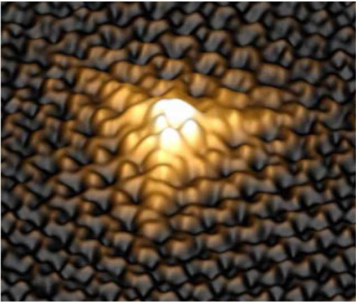
The simplest defect in any material is the missing lattice atom. Single vacancies in graphene have been experimentally observed by transmission electron microscopy (TEM) [6,7] and scanning tunnelling microscopy (STM) [8]. Figure 1, for example, shows the local electronic fingerprint of a monovacancy revealed by an STM image, produced on graphite through Ar+ ion-irradiation [8]. Vacancies can also be used as a simplified model for other types of defects that modify the hybridization of the atomic orbitals, such as adsorbates covalently bound to the carbon atoms. This type of disorder has several effects on the electronic structure of graphene, as the introduction of zero energy modes when the vacancies are unequally distributed among the two sublattices [9]. As for transport properties, localization effects have been predicted to be suppressed for disorder that preserves the graphene sublattice symmetry [10]. Vacancies, when equally distributed among the two sublattices, preserve such a symmetry of the system and lead to the saturation of the conductivity at σ0 = 4e2/(πh) when increasing the vacancy density [11,12]. This behaviour suggests the suppression of localization phenomena. However, these theoretical predictions were obtained in the semi-classical limit, while other recent studies on hydrogenated graphene [13,14] have shown that the finite value of the conductivity is not robust in the quantum regime.
In this paper, we explore the effect of single vacancies on the transport properties of two dimensional (2D) graphene and finite graphene flakes within highly doped contacts. Both of these configurations allow us to investigate a relatively wide energy region around the Dirac point, thus clarifying many aspects of the impact of vacancies on different transport regimes and in particular the diffusive regime of 2D samples and the pseudodiffusive regime typical of graphene tunnel junctions [15]. We analyse the role played by different parameters, such as the vacancy density, their distribution on the sublattices and, for the tunnel junctions, different geometries. Our results are summarized by some general scaling behaviour that we identified.
This paper is organized as follows. Section 2 describes in detailed the 2D and tunnel junction graphene configuration and briefly illustrates the simulation methodologies we adopted. Section 3 presents the numerical results and their interpretation. Finally, Section 4 concludes.
2. System Description and Methodology
To describe graphene, we adopt a single orbital pz tight-binding model. The Hamiltonian of a pristine graphene layer reads
A vacancy in the honeycomb lattice leaves three dangling bonds, which might eventually recombine into one double bond and one dangling bond. Here, we will consider non-reconstructed vacancies with passivated dangling bonds. We model the vacancies accordingly, by simply removing the pz orbitals at the vacancy sites from the Hamiltonian (1). This model, which obviously does not hold for real vacancies, is a good approximation for pseudo-vacancies generated, for example, by adsorbates that re-hybridize the orbitals of the carbon from sp2 to sp3. Thanks to its generality, this model has been commonly used in the literature. Note that we do not take into account the spin degree of freedom, because here we focus only on the interplay between sublattice symmetry and electronic transport. The role of vacancies in inducing the magnetization of graphene (widely investigated in the literature [16–20]) is beyond the scope of this study.
The specific repartition of the vacancies among the two sublattices is a crucial aspect of our study. In fact, by using the rank-nullity theorem, it has been shown [9] that an imbalance of vacancies between the A and B sublattices induces zero energy modes. The demonstration is valid only for inter-orbital coupling limited to first-neighbours and it is as follows. Consider a bipartite system with NA sites on the A sublattice and NB on the B sublattice. Without loss of generality, we consider NA > NB. The number of imbalanced vacancies is given by NV = NA − NB. The Hamiltonian can be decomposed into its projections onto the A and B subspaces, i.e., , , , and , where ∊A and ∊B are the onsite energies for the A and B sublattices, I is the identity matrix and the size of the matrices is indicated. When the Hamiltonian operates on a generic state ϕ = (ϕA, ϕB) it gives . Since NA > NB, we can find NV linearly independent vectors such that . Therefore, the vectors are eigenvectors of the Hamiltonian with eigenvalues ∊A. In graphene ∊A = 0 and we obtain NV zero energy states strictly confined on the A sublattice.
These states affect the spectrum around the Dirac point. In [9], a gap formation is reported, although not observed in [14] for equal vacancy concentrations, the width of which is predicted to be:
2.1. Electronic Structure and Transport in 2D Graphene: Methodology
Electronic structure calculations are performed using the Lanczos recursion method on a sample of 106 carbon atoms with periodic boundary conditions. This sample size is large enough to allow for a randomisation of the distribution of vacancies. The parameters for the Lanczos calculation are N = 1500 recursion steps and an energy resolution of η = 15 meV.
As concerns electronic transport, to simulate the conductivity in the semi-classical and quantum regimes, an efficient real space implementation for computing the Kubo formula is used. We present here a summary of this technique, with the intent to make the interpretation of the results illustrated later on in this paper easier. One starts with an alternative expression of the Kubo conductivity [21–27]
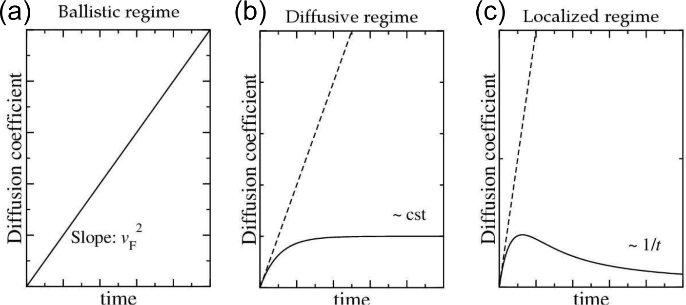
Ballistic regime. Electrons travel through the systems without suffering any scattering, so that DE(t) and XE(t) are linear functions of time, with slopes respectively equal to and vF.
Diffusive regime. It is characterized by a saturation of DE(t→∞). The saturation value identifies the elastic relaxation time τ.
Localized regime. It is manifested by an increasing contribution of quantum interferences that reduce the diffusion coefficient, which roughly scales as ∼ 1/t. The spreading XE(t) reaches an asymptotic value related to the localization length ξ(E).
All the dynamics of the electronic system is actually conveyed by the operator. Since the Hamiltonian accounts for the presence of static disorder (e.g., randomly located defects), the time-dependent quantum dynamics of electronic wavepackets capture all multiple scattering phenomena including those accessible within the semi-classical transport regime (Bloch–Boltzmann) such as the elastic mean-free-path, or within the quantum interferences regime such as the localization length.
We applied the Kubo real space algorithm, using elapsed times of 1100 steps of 0.23 fs each. This provides an accurate description of quasi-ballistic and diffusive regimes, together with the quantum regime in which multiple scattering phenomena yield interferences and localization. The maximum evolution time of the random phase state is about 2.7 ps. The sample, a rectangular sheet of 21.2 nm × 12.2 nm, is chosen large enough so that the electron wavepacket propagates without reaching the edges of the sheet, thus minimizing finite-size effects. For each concentration and distribution of vacancies, we calculate the maximum of the diffusion coefficient Dmax(E), the mean free path ℓe(E) and the Fermi velocity vF(E), from which we infer the semi-classical conductivity in the diffusive regime σSC. Then we derived the conductivity at latter times to take into account quantum interferences (and localization phenomena), using the approximation:
2.2. Electronic Transport in Graphene Tunnel Junctions: Methodology
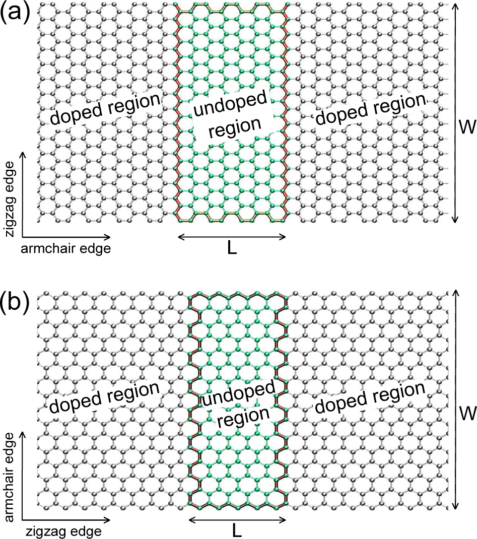
In the tunnel junction configuration, the system consists of a large armchair graphene nanoribbon (aGNR) or zigzag graphene nanoribbon (zGNR) with width W, see Figure 3, with highly doped contacts and an undoped section of length L. The doping is obtained by setting a superimposed potential V on the doped regions. In our simulations, we choose V = −1.5 eV, this entailing a n-type doping.
We will consider the presence of compensated/uncompensated vacancies uniformly distributed within the undoped region with density n. The conductivity of the system is indicated as σ(E, L, W, n) = (2e2/h) × T (E, L, W, n) × L/W, where E is the energy of the injected electrons and T is the transmission coefficient obtained by the standard Landauer–Büttiker formula within the Green’s function approach
The corresponding resistivity is ρ(E, L, W, n) = 1/σ(E, L, W, n). When n = 0, i.e., for the pristine system, the intrinsic conductivity and resistivity are σint(E, L, W ) ≡ σ(E, L, W, n = 0) and ρint(E, L, W) ≡ ρ(E, L, W, n = 0). For large W/L ratios and energies E around the Dirac point, the system exhibits a pseudodiffusive transport regime [15,31–36], where the conductive channels of the contacts tunnel through the undoped region a with constant minimum conductivity σint(E ≈ 0, L, W ≫ L) ≈ 4e2/(πh) = σ0. The term pseudodiffusive indicates that the system behaves as if it were in a diffusive regime, even though no disorder is present and the diffusive behaviour is only mimicked by the peculiar values of the transport coefficients of the tunnelling conduction channels.
For n > 0, we define the extrinsic quantities ρext(E, L, W, n) ≡ ρ(E, L, W, n) − ρint(E, L, W ) and σext(E, L, W, n) ≡ 1/ρext(E, L, W, n). As we will see, at E = 0 and in the presence of compensated vacancies, the conductivity may increase, thus entailing a negative extrinsic resistance.
3. Results and Discussion
We investigated several concentrations of vacancies n up to 2%, for the two cases where the vacancies were equally distributed among the two sublattices (AB) or on one sublattice only (AA). Subsections 3.1 and 3.2 contain the results for 2D graphene. Subsection 3.3 reports on the case of graphene tunnel junctions. As illustrated and analysed below, the results for 2D graphene and graphene tunnel junctions are in agreement and they reveal different facets of the same physics.
3.1. Electronic Structure of 2D Graphene with Vacancies
The intrinsic density of states of 2D graphene increases linearly with energy and vanishes at the Dirac point. As briefly discussed above, vacancies are expected to impact the DOS especially at low energy with the formation of zero energy states. To better illustrate their impact, we consider here the extrinsic density of states, which is given by the difference between the DOS in the presence of vacancies and that for pristine graphene.
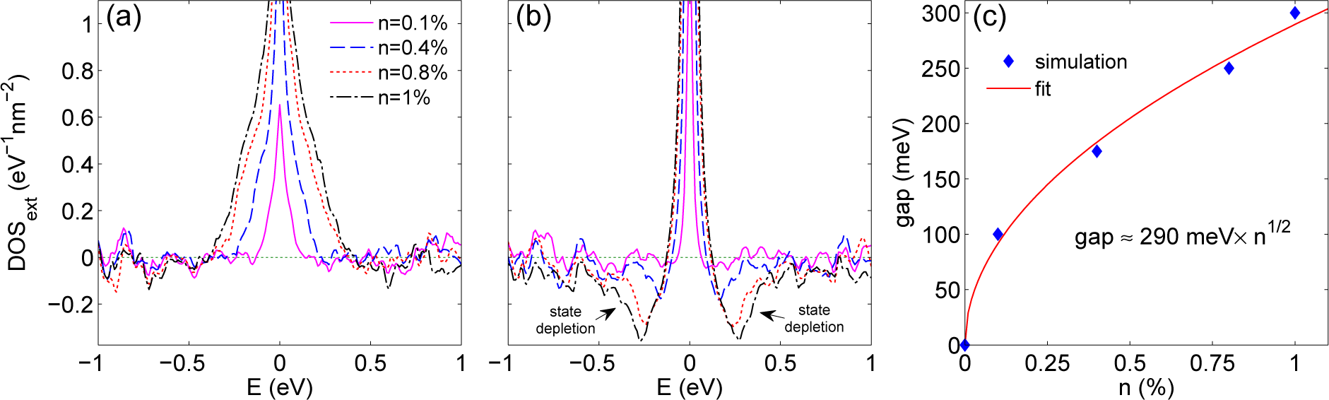
Our results for the extrinsic DOS in the compensated (AB) case are plotted in Figure 4a for concentrations from 0.1% to 1%. We observe that the DOS increases around the Dirac point over an energy region that is larger for higher densities. Outside this region, the extrinsic DOS fluctuates around 0, meaning that the total DOS is not significantly modified with respect to the clean case. Although the DOS seems to increase considerably in correspondence to the Dirac point, as in [9] our numerical resolution is clearly not good enough to investigate what happens exactly at E = 0.
The extrinsic DOS in the uncompensated (AA) case are plotted in Figure 4b, for the same vacancy densities. As expected, the breaking of A-B symmetry generates a relatively sharp peak at zero energy. The peak height increases with vacancy concentration and this occurs at the expense of the DOS at the sides of the Dirac point, where the extrinsic DOS becomes negative. Although we cannot yet be conclusive about this point, it could be the effect of a gap opening, partially hidden by the wings of the convoluted zero-energy peak. This could explain contradictory observations as reported in [9,14]. Reference [9] pinpoints the opening of an energy gap, whereas [14] suggests the absence of localization in the uncompensated case for energies close to Fermi level. Figure 4c shows our estimation of the simulated gap against n and its fit, which gives
In both AB and AA cases, vacancies preserve the hole-particle symmetry (chiral symmetry) and affect the electronic structure around the Dirac point, although in a different manner. In the first case the DOS increases, while for the AA distribution there is a depletion of the DOS around Fermi energy and a finite concentration of zero-energy modes in the middle.
3.2. Electronic Transport in 2D Graphene with Vacancies
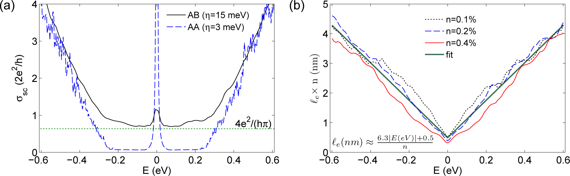
We start by illustrating the results for the semi-classical conductivity and mean free path summarized in Figure 5. We consider a vacancy density n = 0.8% for both the compensated and the uncompensated case. The corresponding semi-classical conductivities as a function of the electron energy are reported in Figure 5a. Away from Dirac point and in both of the cases, σSC increases linearly with energy with very similar values. On the contrary, around the Dirac point the results for compensated and uncompensated vacancies are very different and are strictly connected to what was already observed for the DOS. For the balanced case (continuous line), σSC exhibits a large plateau above the value σ0 = 4e2/(πh) (dotted line). This result confirms what was theoretically predicted in [11] and previous observations [12]. Moreover, a conductivity peak is present exactly around the Dirac point, as the result of the presence of the zero-energy vacancy-generated states. However, it would be erroneous to conclude that no localisation phenomena occur in this energy region. In fact, for longer simulation time, i.e., when going beyond the maximum diffusion coefficient, the conductivity progressively decreases below the theoretical minimal value for semi-classical conductivity σ0. We will discuss this aspect later on in terms of the time evolution of the Kubo diffusion coefficient.
For unbalanced vacancies (dashed curve), we can clearly observe a conductivity gap and, again, a very marked peak around E = 0. Note that, in this case, we adopted a higher energy resolution (η = 3 meV) in order to have a better accuracy in the region of the gap. This also entails the presence of many fluctuations visible at higher energy. For lower resolution, not shown here [37], the plateau is higher (not much below σ0) and the peak at the Dirac point is reduced. Such a phenomenon is because the energy resolution drives the DOS to zero around Dirac point while the zero-energy peak is increased. This evolution towards a gap when decreasing the resolution confirms the results presented in [9]: In the limit of zero temperature (which can be modelled by η → 0) the system will become insulator, with the peculiar feature of presenting a finite concentration of mid-gap states. Such a gap opening was not observed in [14] for low concentrations, presumably because of a lack of energy resolution.
Figure 5b shows the mean free path multiplied by the vacancy density as a function of the energy for compensated vacancies. We observe that all the curves almost superimpose, meaning that ℓe roughly scales as 1/n, as expected for much diluted scatterers. We also observe that the mean free path scales linearly with energy and this allows us to infer the scaling law
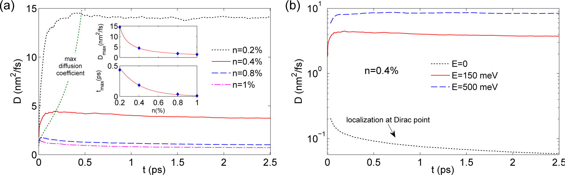
To better understand the physics of vacancies at the Dirac point, we now consider the evolution of the Kubo diffusion coefficients as a function of time. We focus on the case of compensated vacancies. Figure 6a shows the diffusion coefficient at the energy E=150 meV and for vacancy densities between 0.2% and 1%. We can clearly distinguish the different transport regimes schematized in Figure 3. In particular, we observe that the maximum diffusion coefficient Dmax (corresponding to the semi-classical value) occurs at shorter times tmax for higher densities and it assumes lower values, as expected from the mean free path behaviour, see Figure 5b. The estimated position of the maxima of the diffusion coefficient is indicated by a dashed line in the figure. After this line, D starts decreasing, more or less slowly, toward the localisation regime. Depending on the speed of such a decrease, we can determine whether a transition between the two transport regimes is expected.
For example, and much interestingly, we examine what happens to the diffusion coefficients for a given density of compensated vacancy and at different energies close and far from the Dirac point.
Figure 6b focuses on the case n = 0.4%. At energies far from the Dirac point, the decay of the diffusion coefficient is very slow, indicating that the system is in the diffusive transport regime. Close to the Dirac point, on the contrary, the behaviour is very different. First of all, the maximum diffusion coefficient is much smaller than away from E = 0. This might appear to be in contrast with the zero-energy peak of the semi-classical conductivity observed in Figure 5a. However, we have to consider that this peak is the combined result of an extremely high DOS and a relatively low Dmax. The second difference is that the diffusion coefficient at the Dirac point decreases considerably with time. Such a result clearly indicates that the transport regime at the Dirac point undergoes a transition from diffusive to strongly localized.
3.3. Electronic Transport in Graphene Tunnel Junctions with Vacancies
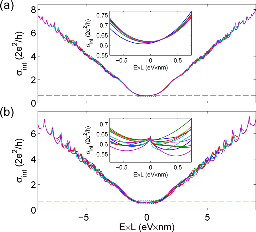
Let us start this section by briefly illustrating the results for the intrinsic transport properties of the system, i.e., in the absence of vacancies. As seen in Figure 3, the undoped region between the two highly-doped contacts is a ribbon section with edges W and L. For given width W (< L) of the system, the number of active conductive channels M(E, L) in the undoped section is thus determined by the energy E and the length L. If the system has armchair edges, the nanoribbon section has two armchair edges with length L and two zigzag edges with length W, see Figure 3a. Therefore, the number of conductive modes varies as the number of modes in a zigzag nanoribbon with width L. At low energies, M(E, L) = Mzigzag(E × L) depends only on the product E × L. If the system has zigzag edges, the nanoribbon section has two armchair edges with length W and two zigzag edges with length L, see Figure 3a. Similarly to the prior case, the number of conductive modes varies as the number of modes in an armchair nanoribbon with width L. At low energies, M(E, L) = Marmchair(E × L) changes for different armchair ribbon families, represented by ribbons consisting of 3n, 3n+1 or 3n+2 dimer lines, with n an integer number. Therefore, L determines the energy scale of the region around the minimum conductivity, where we expect that, for W > L and E close to 0, σint(E, L, W ) and ρint(E, L, W) are universal functions of E × L. At higher energy, a larger frequency component scaling with E × W develops due to the progressive opening of the sub-bands corresponding to transverse confinement [32]. This behaviour is confirmed by Figure 7, where all curves are seen to collapse onto a universal curve under appropriate rescaling.
Note that in Figure 7a the minimum conductivity does not lie exactly at E = 0 due to the fact that the DOS of the doped contacts is not symmetric with respect to E = 0, whereas its magnitude is slightly lower than the universal value σ0. For the case of the zGNRs (see Figure 7b), a small peak around E = 0 is seen. This is due to the transmission of the electrons through the first (edge) mode of the zigzag system [38], which is also active at low energy in the undoped region. At E = 0 the bands in the zigzag undoped region are almost flat, the density of states is very high and this explains the peak. The asymmetry is due to the fact that the obtained asymmetry is driven by the change from a n-p-n to a n-n-n heterojunction (as for the aGNRs).
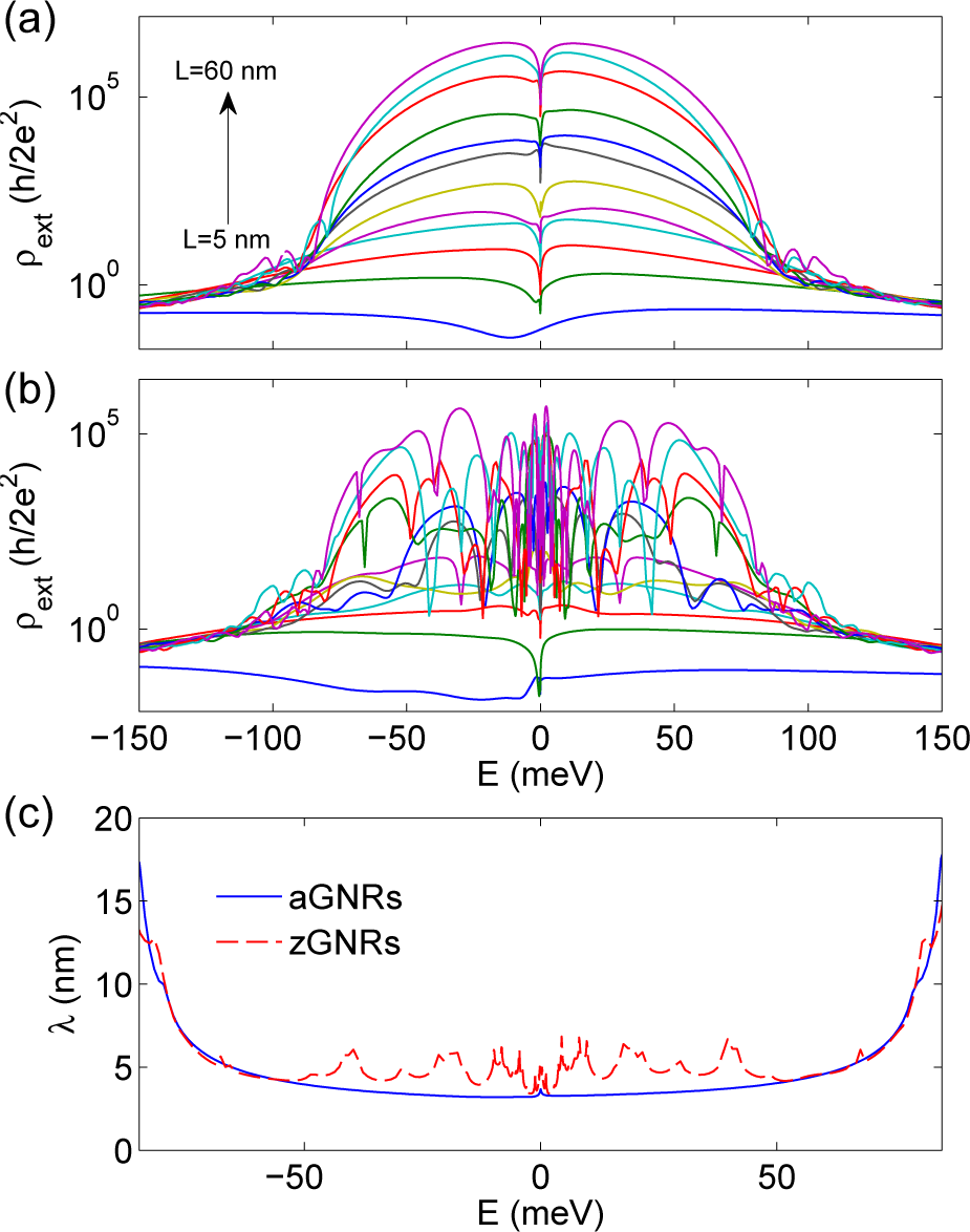
Let us now consider the presence unbalanced vacancies in the undoped region. As seen for 2D graphene in Figure 4b, when increasing n = nA > 0 (nB = 0), zero energy states emerge together with a DOS decay in a certain region around the Dirac point, which is anticipated as a gap formation. We first consider aGNRs with W = 150 nm, L ∈ [5, 60] nm and n = 0.1% = 3.82 × 10⁻² nm−2. The transport results are reported in Figure 8a and show the raise of a dip in the extrinsic resistivity exactly at E = 0, due to the presence of the highly localized zero energy states caused by the vacancies. These states can interact with the very low energy states of the first band of the zigzag nanoribbon corresponding to the undoped region, which decay exponentially along each sublattice when moving from the edges to the bulk, thus enhancing tunnelling. When L increases, the DOS in the centre of the undoped region decreases with a subsequent tunnelling suppression. However, the dip remains well-visible in the figure due to the stronger increase of the resistivity in the remaining region of the gap. We next consider zGNRs with W = 150 nm, L ∈ [5, 60] nm and n = 0.1% = 3.82 × 10⁻² nm−2. The results are reported in Figure 8b. In addition to what was observed for the aGNRs, many resonances appear in the region of the gap and increase in number for longer L. This can be explained by considering the edge states corresponding to the zigzag edges of the section. The coupling of these extended low energy states with the zero energy states due to vacancies give rise to the observed peaks.
In the gap region, the extrinsic resistivity increases exponentially, i.e., ρext ∝ exp (L/λ). Figure 8c shows the estimated values of λ for the aGNRs and the zGNRs as a function of the energy in the region of the gap. For both aGNRs and zGNRs, we have λ ≈ 5 nm. It is important to notice that the gap width is independent of the ribbon chirality, and it is of the same order of that found for 2D graphene, see Figure 4c. The scaling of the gap with n1/2, not shown here, is also verified for ribbons [37].
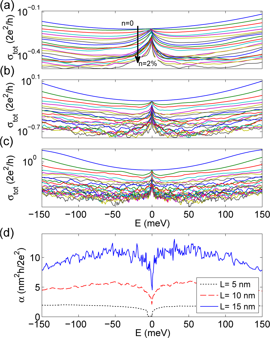
Finally, we consider the case of compensated vacancies. We focus on aGNRs with width W = 150 nm, length of the undoped region L = 5, 10 and 15 nm, and density of vacancies n from 0 up to 2%. The average conductivity (over 20 different disorder realizations) is reported in Figure 9a–c as a function of the energy for the three considered lengths. The average over different random configurations is actually necessary due to the extreme variability of the results depending on the specific configuration of disorder [37]. In all cases, we can clearly observe a conductivity peak at E ≈ 0, which again stems from the formation of zero-energy vacancy induced states. However, in contrast to what was observed for uncompensated vacancies, the gap does not open and the induced states have a broader energy, which entails a broader peak. For a single disordered configuration, the height of the peak can be occasionally larger than σ0, thus determining an enhanced conductivity with respect to the pristine system.
From the analysis of the data, it turns out that, away from the Dirac point, the average extrinsic resistivity is roughly proportional to n, i.e., < ρext(E, L, W, n) ≥ α(E, L, W) × n, at least at the low densities here considered and as long as the resistivity is not too high. The estimated α is shown in Figure 9d. Around E = 0, α decreases and indeed the linear behaviour of the extrinsic resistivity is limited to low densities, while it becomes sublinear at higher densities, thus indicating the slower decay of the minimum conductivity at the Dirac point.
A further analysis shows that ρext = f(E × L, n × L2 × β), where β = 1 around E = 0 and it slightly increases with L elsewhere. The dependence on E × L is related to the activation of the energy bands in the undoped region, as already discussed. The scaling with n × L2 indicates that the extrinsic resistivity depends on the square of χ = n1/2 × L = L/ζ, which is the average number of impurities (per unit of ribbon width) that an electron is expected to meet when crossing the undoped region.
To verify this scaling, in Figure 10, ρext is plotted as a function of n × L2 for some selected values of E × L. Note that, due to rescaling, the available data cover smaller regions for larger L. Figure 10 summarizes some of our main results: (i) the reduced extrinsic resistivity at the Dirac point with respect to the other energy regions; (ii) the approximately linear dependence of the extrinsic resistivity on the defect density n; (iii) universal scaling of the average extrinsic resistivity as a function of E×L and n×L at the Dirac point. At higher energies, the superposition of the curves progressively degrades, especially at higher densities for which the rise of the extrinsic resistivity turns out to be faster for short L. This is physically sound, because for short pristine undoped regions, the transport coefficients of individual conductive channels through the evanescent states are higher than for undoped longer regions. Therefore, apart for energies around E = 0 where resonant impurities play a major role, they are proportionally more strongly affected by disorder.
4. Conclusions
We performed a thorough simulation of electronic transport in graphene in the presence of compensated and uncompensated vacancies. We considered the case of 2D graphene, investigated with the real space Kubo–Greenwood approach, and the case of a finite section of graphene ribbon within two highly doped contacts. For 2D graphene, we have found that conventional localization phenomena develop whenever vacancies are distributed at random and in a balanced fashion between both sublattices, and that mean free paths and localization lengths are smaller at the Dirac point. A suppression of DOS and conductivity were obtained for uncompensated distribution of vacancies in a single sublattice. The results for the finite graphene ribbons within doped contacts are qualitatively in agreement with those for 2D graphene. For uncompensated vacancies, a gap opens around the Dirac point, with a conductivity that decreases exponentially with the length of the undoped region. Exactly at the Dirac point and for armchair edge geometry, the resistivity exhibits a dip, which indicates the residual enhanced tunnelling of the electrons through resonant states only existing at zero energy. In the case of zigzag ribbons, many resonances appear in the gap when increasing the length of the undoped region. These are consequences of the coupling between the resonant states and the low energy edge states typical of zigzag ribbons. For compensated vacancies and away from the Dirac point, the average conductivity is found to decrease linearly with the defect density. At low energies, the decrease is much slower and a broad conductivity peak is present. By a scaling analysis, we found that the extrinsic resistivity is a function of the energy times the undoped region length and of the vacancy density times the square of the undoped region length.
Acknowledgments
A.C. acknowledges the support of Fondation Nanosciences via the RTRA Dispograph project. S.R. acknowledges the support from SAMSUNG within the Global Innovation Program.
- Classification: PACS 72.80.Vp, 73.63.-b, 73.22.Pr, 72.15.Lh, 61.48.Gh
References and Notes
- Banhart, F.; Kotakoski, J.; Krasheninnikov, A.V. Structural defects in graphene. ACS Nano 2010, 5, 26–41. [Google Scholar]
- Zhao, L.; He, R.; Rim, K.T.; Schiros, T.; Kim, K.S.; Zhou, H.; Gutirrez, C.; Chockalingam, S.P.; Arguello, C.J.; Plov, L.; et al. Visualizing individual nitrogen dopants in monolayer graphene. Science 2011, 333, 999–1003. [Google Scholar]
- Biel, B.; Blase, X.; Triozon, F.; Roche, S. Anomalous doping effects on charge transport in graphene nanoribbons. Phys. Rev. Lett. 2009, 102, 096803:1–096803:4. [Google Scholar]
- Biel, B.; Triozon, F.; Blase, X.; Roche, S. Chemically induced mobility gaps in graphene nanoribbons: A route for upscaling device performances. Nano Lett. 2009, 9, 2725–2729. [Google Scholar]
- Marconcini, P.; Cresti, A.; Triozon, F.; Fiori, G.; Biel, B.; Niquet, Y.M.; Macucci, M.; Roche, S. Atomistic boron-doped graphene field-effect transistors: A route toward unipolar characteristics. ACS Nano 2012, 6, 7942–7947. [Google Scholar]
- Gass, M.H.; Bangert, U.; Bleloch, A.L.; Wang, P.; Nair, R.R.; Geim, A.K. Free-standing graphene at atomic resolution. Nat. Nanotechnol. 2008, 3, 676–681. [Google Scholar]
- Meyer, J.C.; Kisielowski, C.; Erni, R.; Rossell, M.D.; Crommie, M.F.; Zettl, A. Direct imaging of lattice atoms and topological defects in graphene membranes. Nano Lett. 2008, 8, 3582–3586. [Google Scholar]
- Ugeda, M.M.; Brihuega, I.; Guinea, F.; Gómez-Rodríguez, J.M. Missing Atom as a Source of Carbon Magnetism. Phys. Rev. Lett. 2010, 104, 096804:1–096804:4. [Google Scholar]
- Pereira, V.M. dos Santos, L.; Neto, A.H.C. Modeling disorder in graphene. Phys. Rev. B 2008, 77, 115109:1–115109:17. [Google Scholar]
- Ostrovsky, P.M.; Gornyi, I.V.; Mirlin, A.D. Electron transport in disordered graphene. Phys. Rev. B 2006, 74, 235443:1–235443:20. [Google Scholar]
- Ostrovsky, P.M.; Titov, M.; Bera, S.; Gornyi, I.V.; Mirlin, A.D. Diffusion and criticality in undoped graphene with resonant Scatterers. Phys. Rev. Lett. 2010, 105, 266803:1–266803:4. [Google Scholar]
- Zhu, W.; Li, W.; Shi, Q.W.; Wang, X.R.; Wang, X.P.; Yang, J.L.; Hou, J.G. Vacancy-induced splitting of the Dirac nodal point in graphene. Phys. Rev. B 2012, 85, 073407:1–073407:4. [Google Scholar]
- Soriano, D.; Leconte, N.; Ordejón, P.; Charlier, J.C.; Palacios, J.J.; Roche, S. Magnetoresistance and magnetic ordering fingerprints in hydrogenated graphene. Phys. Rev. Lett. 2011, 107, 016602:1–016602:4. [Google Scholar]
- Leconte, N.; Soriano, D.; Roche, S.; Ordejon, P.; Charlier, J.C.; Palacios, J.J. Magnetism-dependent transport phenomena in hydrogenated graphene: From spin-splitting to localization effects. ACS Nano 2011, 5, 3987–3992. [Google Scholar]
- Tworzydło, J.; Trauzettel, B.; Titov, M.; Rycerz, A.; Beenakker, C.W.J. Sub-poissonian shot noise in graphene. Phys. Rev. Lett. 2006, 96, 246802:1–246802:4. [Google Scholar]
- Palacios, J.J.; Fernández-Rossier, J.; Brey, L. Vacancy-induced magnetism in graphene and graphene ribbons. Phys. Rev. B 2008, 77, 195428:1–195428:14. [Google Scholar]
- Yazyev, O.V. Magnetism in disordered graphene and irradiated graphite. Phys. Rev. Lett. 2008, 101, 037203:1–037203:4. [Google Scholar]
- Kumazaki, H.; Hirashima, D.S. Tight-binding study of nonmagnetic-defect-induced magnetism in graphene. Low Temp. Phys. 2008, 34, 805–811. [Google Scholar]
- López-Sancho, M.P.; de Juan, F.; Vozmediano, M.A.H. Magnetic moments in the presence of topological defects in graphene. Phys. Rev. B 2009, 79, 075413:1–075413:5. [Google Scholar]
- Cazalilla, M.A.; Iucci, A.; Guinea, F.; Neto, A.H.C. Local moment formation and kondo effect in defective graphene, Available online: http://arxiv.org/abs/1207.3135 accessed on 1 February 2013.
- Roche, S.; Leconte, N.; Ortmann, F.; Lherbier, A.; Soriano, D.; Charlier, J.C. Quantum transport in disordered graphene: A theoretical perspective. Solid State Commun. 2012, 152, 1404–1410. [Google Scholar]
- Roche, S.; Mayou, D. Conductivity of quasiperiodic systems: A numerical study. Phys. Rev. Lett. 1997, 79, 2518–2521. [Google Scholar]
- Roche, S. Quantum transport by means of O(N) real-space methods. Phys. Rev. B 1999, 59, 2284–2291. [Google Scholar]
- Roche, S.; Saito, R. Magnetoresistance of carbon nanotubes: From molecular to mesoscopic Fingerprints. Phys. Rev. Lett. 2001, 87, 246803:1–246803:4. [Google Scholar]
- Triozon, F.; Roche, S.; Rubio, A.; Mayou, D. Electrical transport in carbon nanotubes: Role of disorder and helical symmetries. Phys. Rev. B 2004, 69, 121410:1–121410:4. [Google Scholar]
- Ishii, H.; Triozon, F.; Kobayashi, N.; Hirose, K.; Roche, S. Charge transport in carbon nanotubes based materials: A Kubo-Greenwood computational approach. Comptes Rendus Phys. 2009, 10, 283–296. [Google Scholar]
- Latil, S.; Roche, S.; Mayou, D.; Charlier, J.C. Mesoscopic transport in chemically doped carbon nanotubes. Phys. Rev. Lett. 2004, 92, 256805:1–256805:4. [Google Scholar]
- In term of fluctuation-dissipation theory, the motion of an electronic wavepacket due to an external electric field (i.e., dissipation under non-equilibrium conditions) is related to the spreading of the wavepacket without any external electric field (i.e., fluctuations at the equilibrium).
- Random-phase states spread over all the orbitals |n〉 of the basis set and are defined as:where α(n) is a random number in the [0, 1] range. An average over few tens of random phase states is sufficient to calculate the expectation values.
- Grosso, G.; Moroni, S.; Pastori Parravicini, G. Electronic structure of the InAs-GaSb superlattice studied by the renormalization method. Phys. Rev. B 1989, 40, 12328–12337. [Google Scholar]
- Katsnelson, M.I. Zitterbewegung, chirality, and minimal conductivity in graphene. Eur. Phys. J. B 2006, 51, 157–160. [Google Scholar]
- Cresti, A.; Grosso, G.; Parravicini, G.P. Numerical study of electronic transport in gated graphene ribbons. Phys. Rev. B 2007, 76, 205433:1–205443:8. [Google Scholar]
- Robinson, J.P.; Schomerus, H. Electronic transport in normal-conductor/graphene/normal-conductor junctions and conditions for insulating behavior at a finite charge-carrier density. Phys. Rev. B 2007, 76, 115430:1–115430:11. [Google Scholar]
- Blanter, Y.M.; Martin, I. Transport through normal-metal-graphene contacts. Phys. Rev. B 2007, 76, 155433:1–155433:6. [Google Scholar]
- Miao, F.; Wijeratne, S.; Zhang, Y.; Coskun, U.C.; Bao, W.; Lau, C.N. Phase-coherent transport in graphene quantum billiards. Science 2007, 317, 1530–1533. [Google Scholar]
- Danneau, R.; Wu, F.; Craciun, M.; Russo, S.; Tomi, M.; Salmilehto, J.; Morpurgo, A.; Hakonen, P. Evanescent wave transport and shot noise in graphene: Ballistic regime and effect of disorder. J. Low Temp. Phys. 2008, 153, 374–392. [Google Scholar]
- Cresti, A.; Ortmann, F.; Van Tuan, D.; Louvet, T.; Roche, S. Catalan Institute of Nanotechnology (CIN2), Universitat Autónoma de Barcelona, Campus UAB, Bellaterra 08193, Spain ; Institució Catalana de Recerca i Estudis Avançats (ICREA), Barcelona 08070, Spain, Unpublished work. 2013.
- Cresti, A.; Nemec, N.; Biel, B.; Niebler, G.; Triozon, F.; Cuniberti, G.; Roche, S. Charge transport in disordered graphene-based low dimensional materials. Nano Res 2008, 1, 361–394. [Google Scholar]


© 2013 by the authors; licensee MDPI, Basel, Switzerland This article is an open access article distributed under the terms and conditions of the Creative Commons Attribution license (http://creativecommons.org/licenses/by/3.0/).
Share and Cite
Cresti, A.; Louvet, T.; Ortmann, F.; Van Tuan, D.; Lenarczyk, P.; Huhs, G.; Roche, S. Impact of Vacancies on Diffusive and Pseudodiffusive Electronic Transport in Graphene. Crystals 2013, 3, 289-305. https://doi.org/10.3390/cryst3020289
Cresti A, Louvet T, Ortmann F, Van Tuan D, Lenarczyk P, Huhs G, Roche S. Impact of Vacancies on Diffusive and Pseudodiffusive Electronic Transport in Graphene. Crystals. 2013; 3(2):289-305. https://doi.org/10.3390/cryst3020289
Chicago/Turabian StyleCresti, Alessandro, Thibaud Louvet, Frank Ortmann, Dinh Van Tuan, Paweł Lenarczyk, Georg Huhs, and Stephan Roche. 2013. "Impact of Vacancies on Diffusive and Pseudodiffusive Electronic Transport in Graphene" Crystals 3, no. 2: 289-305. https://doi.org/10.3390/cryst3020289