Article

Investigating the Efficiency Droop of Nitride-Based Blue LEDs with Different Quantum Barrier Growth Rates

Department of Electronic Engineering, Southern Taiwan University of Science and Technology, Tainan City 71005, Taiwan
*
Author to whom correspondence should be addressed.
Crystals 2019, 9(12), 677; https://doi.org/10.3390/cryst9120677
Submission received: 14 October 2019 / Revised: 13 November 2019 / Accepted: 13 December 2019 / Published: 17 December 2019
(This article belongs to the Special Issue Recent Advances in Light-Emitting Diodes (LEDs))

Abstract

:
In this study, GaN-based blue InGaN/GaN light-emitting diodes (LEDs) with different growth rates of the quantum barriers were fabricated and investigated. The LEDs with quantum barriers grown with a higher growth rate exhibit a lower leakage current and less non-radiative recombination centers in the multiple quantum wells (MQWs). Therefore, the LED with a higher barrier growth rate achieves a better light output power by 18.4% at 120 mA, which is attributed to weaker indium fluctuation effect in the QWs. On the other hand, the localized states created by indium fluctuation lead to a higher local carrier density, and Auger recombination in the QWs. Thus, the efficiency droop ratio of the LEDs with a higher barrier growth rate was only 28.6%, which was superior to that with a lower barrier growth rate (39.3%).

1. Introduction

Recently, LEDs have been used for many applications, such as full-color displays, exterior automotive lighting, traffic lights, indicators, and cell phones. LEDs are the most important lighting devices in the future due to their advantages in terms of environmental protection, long lifetime, and vivid color. However, some existing mechanisms of the LEDs can still lead to the efficiency droop effect, such as electron overflow loss [1,2,3], lacking in hole injection [4,5], Auger recombination [6,7,8], carrier delocalization [9,10], junction heating [11], and current crowding [12].
In the past several years, many studiees have reported different kinds of electron blocking layer (EBL) of the LEDs in the literature to improve these problems, such as shortperiod superlattice (SPS) EBL with AlGaN/GaN structure, SPS EBL with graded-composition [13,14,15], and p-AlInGaN or p-AlInN EBL [16], which can inhibit the effect of electron overflow and enhance the ability of hole injection to diminish the efficiency droop effect. Iveland et al. reported the effect of efficiency droop in GaN-based LEDs that originated from the excitation of Auger recombination processes by using electron emission spectroscopy to detect the Auger electrons [6]. Galler et al. reported that when using the recombination rate equation (i.e., R = An + Bn2 + Cn3, ABC model), the dominant physical mechanism of the efficiency droop was superlinear in the carrier density of electron and can thereby be attributed to Auger recombination [7]. Delaney et al. illustrated that Auger recombination was really an important damage mechanism in the InGaN quantum wells by the calculations of the Auger recombination process [8]. Then, Yang et al. reported that the quantum efficiency and peak shift were dependent on the injection currents and exhibited a significant function of the indium alloy composition in the MQWs. Such a result offered strong evidence that the delocalization was the primary loss mechanism of the efficiency roll-off in InGaN-based LEDs [9].
As mentioned previously, the efficiency droop effect limits the use of the LEDs especially, in the case of application of a high current density. Therefore, we need to further improve the effect of efficiency droop of the LEDs. In our study, GaN-based InGaN/GaN MQW blue LEDs with different growth rates of the quantum barriers were fabricated. It is reported by Keller et al. that by using 12 pair MQW structures with 3 nm thick InGaN well and 4.5 nm thick GaN barrier, indium at a lower growth rate of GaN barrier can desorb from some areas of the InGaN well, which will cause a lower well indium content and a higher compositional non-uniformity [17]. Therefore, by modulating the growth rates of the quantum barriers, it will be expected that the injection carrier behavior in the MQWs can be improved, thus the quantum efficiency and efficiency droop of the LEDs were also investigated.

2. Experimental

The epitaxial layers of the samples used in our study were all grown on c-plane (0001) sapphire substrates by AIXTRON metal-organic chemical vapor deposition (MOCVD) system with Close Coupled Showerhead technology. About the MO source of epitaxial growth, trimethylgallium (TMGa) (Cassen, Hsinchu, Taiwan), trimethylindium (TMIn) (Cassen, Hsinchu, Taiwan), trimethylaluminum (TMAl) (Cassen, Hsinchu, Taiwan), and ammonia (NH3) (Praxair, Hsinchu, Taiwan) were used as gallium, indium, aluminum, and nitrogen sources, respectively. Disilane (Si2H6) (Praxair, Hsinchu, Taiwan) and biscyclopentadienyl magnesium (CP2Mg) (Cassen, Hsinchu, Taiwan) were used as the doping sources of the n- and p-type GaN, respectively. First of all, a 30 nm thick GaN buffer layer was grown on top of the sapphire substrate at low temperature of 550 °C. Then, a 3 µm thick un-doped GaN layer and a 2 µm thick Si-doped n-GaN layer were grown at 1050 °C. After that, the pre-strain layer with 20 pairs and a lower indium composition InGaN/GaN structure was grown at 900 °C. Then, the carrier recombination centers of InGaN/GaN MQWs were grown. The active region of the MQWs consisted of six pairs of InGaN QW layers with 3 nm thickness and GaN quantum barrier with 6 nm thickness, which were grown at 800 and 910 °C, respectively. The growth rates of the GaN quantum barrier layers labeled LED I, LED II, and LED III were 15, 11.25, and 7.5 Å/min, respectively, which were achieved by a change in III/V ratio. Finally, a 30 nm thick Mg-doped p-AlGaN electron EBL and an 80 nm thick Mg-doped p-GaN layer were all grown at 1000 °C. In order to activate the p-AlGaN and p-GaN layers, the as-grown epitaxial wafers were all further annealed at 650 °C by the furnace in an N2 ambient atmosphere.
For the process of the LED chip, the chip size was 580 × 1140 μm2, which was defined by using standard photolithography. The mesa of the LED chip was performed by dry etching until the 2 μm thick n-GaN layer was exposed. Then, the RF sputter system was used to deposit a transparent and conductive indium tin oxide (ITO) layer with 70 nm thickness onto the p-GaN layer, which can serve as the p-type ohmic contact material, current spreading film, and transparent layer. Next, we used the e-beam evaporator to deposit an Ni/Au (30/500 nm) metal contact layer as the p-electrode on the ITO layer, and a Ti/Al/Ti/Au (15/450/50/500 nm) metal contact as the n-electrode on the exposed n-GaN layer. After that, the backside of a 2 inch sapphire substrate with epitaxial layers were polished down to about the thickness of 90 μm. Finally, the LED chips were performed by dicing saw. After the chip process, the TO-39 metal cans without epoxy resin or silicone for LED encapsulation are used to package these fabricated LED chips, which can collect the emission light. The integrating sphere detector (Forter Tech, Tainan, Taiwan) can be used to measure the light output powers (LOPs) of the fabricated LEDs. The current–voltage (I–V) curves of these fabricated LEDs were all measured by a semiconductor parameter analyzer of HP4156C.

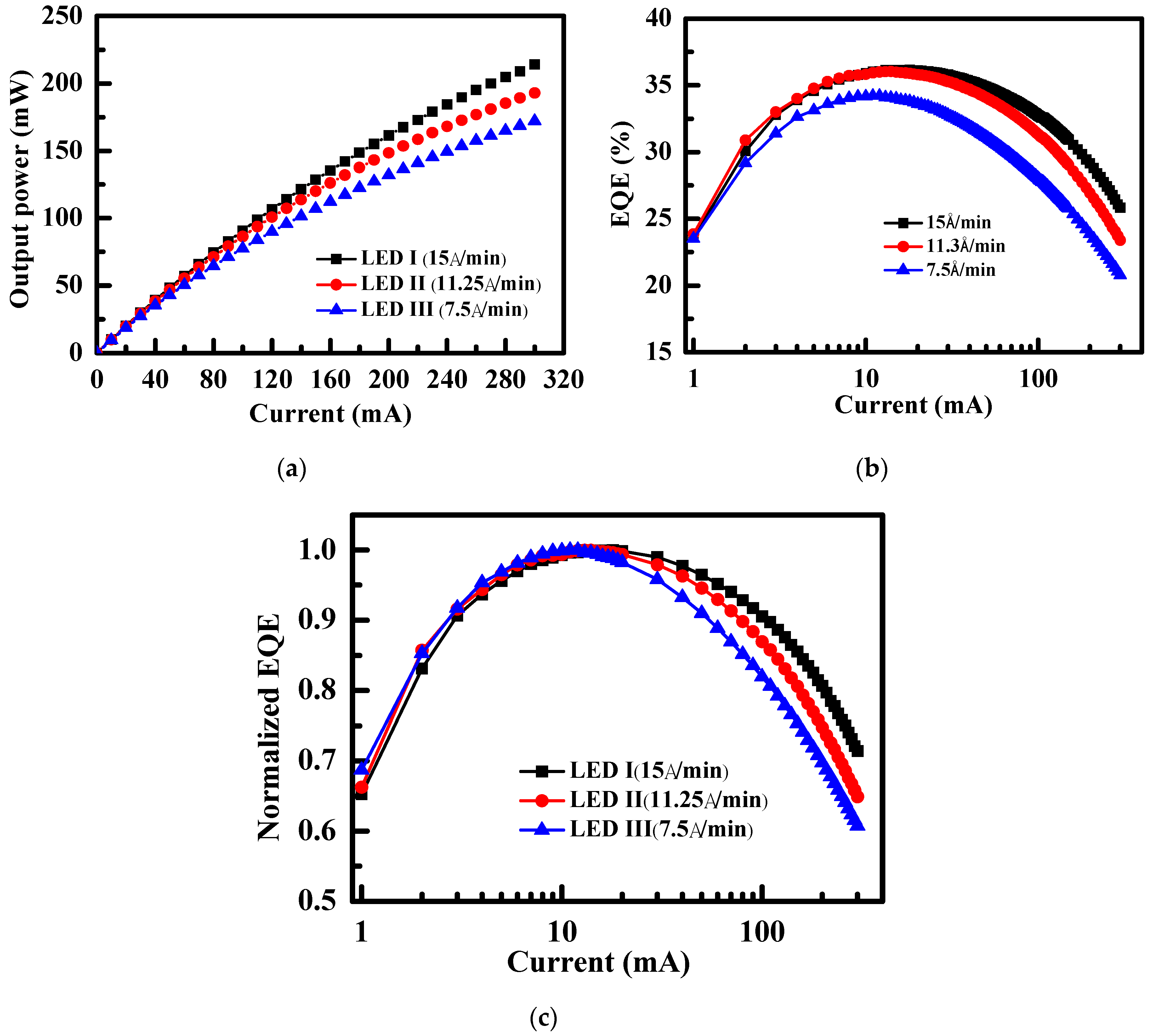
3. Results and Discussion

The LOPs, external quantum efficiency (EQE), and normalized EQE of the fabricated LEDs on a linear and log I scale as shown in Figure 1a–c, respectively. As shown in Figure 1a, the LOPs of LED I, LED II, and LED III were 106.6, 100.7, and 90.0 mW at 120 mA, respectively. In addition, the LOP of LED I at 120 mA was enhanced by 5.9% and 18.4% compared with LED II and LED III, respectively. It was evident that LED I exhibited a superior LOP. Otherwise, the LOPs of LED I, LED II, and LED III were 214.2, 192.9, and 172.0 mW at 300 mA, respectively. As compared with LED II and LED III, the LOP of LED I was improved by approximately 11.0% and 24.5% at 300 mA, respectively. The same tendency is also shown in Figure 1b. The differences of LOP and EQE between the fabricated LEDs evidently became significantly larger especially, at higher injection currents. Then, as shown in Figure 1c, normalized EQE can more clearly compare the differences of the efficiency droop. It was found that the EQE decay percentages from maximum EQE to EQE at 300 mA of LED I, LED II, and LED III were 28.6%, 35.1%, and 39.3%, respectively. Such a result once again pointed out that the optical properties of LED I were superior to those of the others whether operating at low or high injection currents. The physical mechanism of this phenomenon will be proposed in the following paragraphs in detail.
Figure 2 shows the forward current–voltage characteristics on a semilogarithmic scale. It is obvious that the forward current of LED III under the forward bias voltage of 2.4 V is larger than that of the other LEDs. According to the equivalent circuit model of the pn junction diode [18], LED III— with a smaller parallel resistance—is attributed to a larger leakage current. It is pointed out that the excess current of LEDs generated at a voltage of less than 2.4 V is attributed to the minority carrier recombination by the traps in the depletion region most likely related to the V-defects in the MQWs, which arise from the heterointerfaces between the wells and barriers [19,20]. Figure 3a,b shows the (002) and (102) double-crystal X-ray diffraction (DCXRD) spectra of LED I and LED III, respectively. It can be seen clearly that both the main and satellite peaks of (002) XRD spectrum of LED I exhibit larger intensity and narrower full-width at half-maximum (FWHM) than those of LED III in Figure 3a. The same results are also shown in (102) XRD spectrum. The superior X-ray (102) characteristic of LED I implies a lower V-pits density forms along the threading dislocations. Such a result demonstrates that the crystal quality of MQWs of LED I with a higher barrier growth rate is better than that of LED III, which corresponds to the forward I–V characteristics, as mentioned above.
Then, we present an in-depth approach to analyze the non-radiative recombination in the MQW region by the cathodoluminescence (CL) system. The CL spectra of these three LEDs (not shown here) include a weaker GaN near-band-edge (NBE) emission (i.e., 365 nm), a stronger InGaN/GaN MQWs emission (i.e., 450 nm), and a broad yellow band (YL) emission (i.e., 550 nm). Figure 4a,b shows the CL mapping images of the LED I and III recorded at an MQW emission wavelength of 450 nm, respectively. It is clearly evident that LED I has more light spots than LED III. According to the literature, the V-defects in the MQW can act as non-radiative recombination centers and generate the dark areas in the CL images [21,22]. The results obtained demonstrate that LED III has a greater V-defect density and larger leakage current, which also corresponds to the results of Figure 2 and Figure 3. This could be attributed to the fact that the growth temperature of the quantum barriers was 110 °C higher than that of the quantum wells. In order to suppress the generation of V-pits in the MQWs and enhance the carrier confinement capability of MQWs, the growth temperature of the quantum barrier was higher than that of QW, and growth rate of the quantum barrier was decreased. However, if the growth temperature and rate of the quantum barrier are too high and low, respectively, the indium fluctuation effect [23,24] in the MQWs can be induced, which will result in the defect generation (i.e., non-radiative recombination centers) and crystal quality degradation of the MQWs. On the basis of the above, we choose a compromise, which is the reduction of the growth time (i.e., increase the barrier growth rate appropriately) at 910 °C. LED I increases the barrier growth rate appropriately (i.e., still able maintain a good-quality crystal of the barrier–well heterointerfaces in the MQWs) and reducing the barrier growth time in the high-temperature environment can reduce the thermal budget to mitigate the effect of indium fluctuation. According to the equation of the recombination rate for LEDs (i.e., R = An + Bn2 + Cn3), the Shockley–Read–Hall (SRH) recombination (An) and the radiative recombination (Bn2) are dominant recombination mechanisms at a lower current injection density. Such a result evidences that the LOP and EQE of LED I in Figure 1 are the best at lower injection currents.
Figure 5a–c show the temperature-dependent electroluminescence (EL) spectra of LED I, LED II, and LED III, respectively, cooled from 300 K down to 10 K at 5 mA by Helium compressor system and the temperature was controlled by the temperature sensor and heat controller. The similar tendency of temperature-dependent EL intensity of these three fabricated LEDs was observed. As the temperature went down from 300 K, the light intensity of the emission for the LEDs increased. This is attributed to the reduction of the non-radiative recombination rate in the MQW. In other words, the carrier capture rate by the defects will decrease as the temperature decreases [25]. Therefore, the internal quantum efficiency (IQE) of the fabricated LEDs will be increased. Then, the light intensity of the emission began to drop as the temperature kept decreasing due to the reduction of electron and hole concentrations [26]. On the other hand, it was found that the light intensity and FWHM of the emission spectrum for LED III were smaller and wider than those of the other two. In addition to this, it can also be observed that LED III displayed a more evident emission sub-peak than those of the other two around the wavelength of 460 nm. Furthermore, as the ambient temperature decreases, the intensity of the sub-peak has a more significant proportion in the emission spectrum in Figure 5c. This is because when the ambient temperature is lower, the injected carriers into the MQWs are more easily attracted and confined in the localized states with lower potential energy and the longer light wavelengths are emitting. It is suggested that the localized states in the InGaN/GaN quantum wells are created by random indium alloy fluctuations or indium-rich clusters [23,24], which could be attributed that the growth temperature of the quantum barriers was 110 °C higher than that of the quantum wells. As described in the previous paragraph, the higher growth temperature of the quantum barriers can induce indium fluctuation in the MQWs. In addition, the LEDs with quantum barriers grown with a lower growth rate have a larger strain and piezoelectric polarization field between GaN and InGaN due to the strong lattice mismatch. This is the reason that the lattice constant of the GaN quantum barrier of LED III with a lower growth rate will be closer to the ideal value of GaN bulk than that of LED I, which would result in a larger lattice mismatch between the GaN barrier and InGaN well. Therefore, as the carriers are injected into the MQWs, the localized states with the potential minimum in the QWs created by random indium alloy fluctuations or indium-rich clusters leads to a higher partial carrier density in the QWs, which has a significant effect on the FWHM of the spectrum of emitted light. The Auger recombination procedure in the MQWs is extremely enhanced by the carrier localization mechanism [27]. According to the recombination rate equation of the LEDs (i.e., R = An + Bn2 + Cn3), the Auger recombination (Cn3) is a dominant recombination mechanism at higher current injection density. Thus, the efficiency droop effect induced by Auger recombination will become more serious especially, at higher injection current levels. Therefore, LED III has a more serious carrier localization effect induced by random indium alloy fluctuations. Such a result demonstrates why LED I exhibits the weakest efficiency droop effect in Figure 1b.

4. Conclusions

In summary, GaN-based blue InGaN/GaN LEDs with different growth rates of the quantum barriers were demonstrated. It was found that the LOP of the LED with a higher barrier growth rate was 18.4% higher than the LED with a lower barrier growth rate at 120 mA. The LEDs with quantum barriers grown with a higher growth rate exhibit a lower leakage current and less non-radiative recombination centers in the MQWs from the CL mapping images, which is attributed to a weaker indium fluctuation effect induced by the growth temperature of the quantum barriers 110 °C higher than that of the quantum wells. On the other hand, the localized states in the MQWs created by indium fluctuation lead to a higher local carrier density, which resulted in the Auger recombination in the QWs. Thus, the efficiency droop ratio of the LEDs with a higher barrier growth rate was only 28.6%, which was superior to that with a lower barrier growth rate (39.3%).

Author Contributions

Conceptualization: C.K.W. and Y.Z.C. Methodology: C.K.W. and Y.Z.C. Validation: C.K.W. and H.J.C. Formal Analysis: C.K.W., Y.Z.C. and H.J.C. Investigation: C.K.W., Y.Z.C. and H.J.C. Resources: C.K.W. and Y.Z.C. Data curation: H.J.C. Writing—original draft preparation, Writing—review and editing: C.K.W. Supervision: C.K.W. and Y.Z.C. Project administration: C.K.W. and Y.Z.C. Funding acquisition: C.K.W.

Funding

This research was funded by Ministry of Science and Technology, Taiwan, grant number: MOST 108-2221-E-218-022.

Acknowledgments

This work was supported by the Ministry of Science and Technology under contract no. MOST 108-2221-E-218-022.

Conflicts of Interest

The authors declare no conflict of interest.

References

  1. Kim, M.H.; Schubert, M.F.; Dai, Q.; Kim, J.K.; Schubert, E.F.; Piprek, J.; Park, Y. Origin of efficiency droop in GaN-based light-emitting diodes. Appl. Phys. Lett. 2007, 91, 183507. [Google Scholar] [CrossRef] [Green Version]
  2. Schubert, M.F.; Xu, J.; Kim, J.K.; Schubert, E.F.; Kim, M.H.; Yoon, S.; Lee, S.M.; Sone, C.; Sakong, T.; Park, Y. Polarization-matched GaInN/AlGaInN multi-quantum-well light emitting diodes with reduced efficiency droop. Appl. Phys. Lett. 2008, 93, 041102. [Google Scholar] [CrossRef]
  3. Zhao, H.P.; Liu, G.Y.; Zhang, J.; Arif, R.A.; Tansu, N. Analysis of internal quantum efficiency and current injection efficiency in III nitride light-emitting diodes. J. Disp. Technol. 2013, 9, 212. [Google Scholar] [CrossRef]
  4. Ni, X.; Fan, Q.; Shimada, R.; Özgür, Ü.; Morkoç, H. Reduction of efficiency droop in InGaN light emitting diodes by coupled quantum wells. Appl. Phys. Lett. 2008, 93, 171113. [Google Scholar] [CrossRef] [Green Version]
  5. Wang, C.H.; Chang, S.P.; Chang, W.T.; Li, J.C.; Lu, Y.S.; Li, Z.Y.; Yang, H.C.; Kuo, H.C.; Lu, T.C.; Wang, S.C. Efficiency droop alleviation in InGaN/GaN light emitting diodes by graded-thickness multiple quantum wells. Appl. Phys. Lett. 2010, 97, 181101. [Google Scholar] [CrossRef]
  6. Iveland, J.; Martinelli, L.; Peretti, J.; Speck, J.S.; Weisbuch, C. Direct measurement of Auger electrons emitted from a semiconductor light-emitting diode under electrical injection: Identification of the dominant mechanism for efficiency droop. Phys. Rev. Lett. 2013, 110, 177406. [Google Scholar] [CrossRef]
  7. Galler, B.; Lugauer, H.J.; Binder, M.; Hollweck, R.; Folwill, Y.; Nirschl, A.; Gomez-Iglesias, A.; Hahn, B.; Wagner, J.; Sabathil, M. Experimental determination of the dominant type of auger recombination in InGaN quantum wells. Appl. Phys. Express 2013, 6, 112101. [Google Scholar] [CrossRef]
  8. Delaney, K.T.; Rinke, P.; van de Walle, C.G. Auger recombination rates in nitrides from first principles. Appl. Phys. Lett. 2009, 94, 191109. [Google Scholar] [CrossRef] [Green Version]
  9. Yang, Y.; Cao, X.A.; Yan, C. Investigation of the nonthermal mechanism of efficiency rolloff in InGaN light-emitting diodes. IEEE Trans. Electron. Device 2008, 55, 1771. [Google Scholar] [CrossRef]
  10. Harder, J.; Moloney, J.V.; Koch, S.W. Temperature-dependence of the internal efficiency droop in GaN-based diodes. Appl. Phys. Lett. 2011, 99, 181127. [Google Scholar] [CrossRef]
  11. Chow, W.W.; Crawford, M.H.; Tsao, J.Y.; Kneissl, M. Internal efficiency of InGaN light-emitting diodes: Beyond a quasi-equilibrium model. Appl. Phys. Lett. 2010, 97, 121105. [Google Scholar] [CrossRef]
  12. Liu, H.H.; Chen, P.R.; Lee, G.Y.; Chyi, J.I. Efficiency Enhancement of InGaN LEDs with an n-Type AlGaN/GaN/InGaN Current Spreading Layer. IEEE Electron. Device Lett. 2011, 32, 1409. [Google Scholar] [CrossRef]
  13. Zhang, Y.Y.; Yin, Y.A. Performance enhancement of blue light emitting diodes with a special designed AlGaN/GaN superlattice electron-blocking layer. Appl. Phys. Lett. 2011, 99, 221103. [Google Scholar] [CrossRef]
  14. Lin, B.C.; Chen, K.J.; Han, H.V.; Lan, Y.P.; Chiu, C.H.; Lin, C.C.; Shih, M.H.; Lee, P.T.; Kuo, H.C. Advantages of Blue LEDs With Graded-Composition AlGaN/GaN Superlattice EBL. IEEE Photonics Technol. Lett. 2013, 25, 2062. [Google Scholar] [CrossRef]
  15. Park, J.H.; Kim, D.Y.; Hwang, S.; Meyaard, D.; Schubert, E.F.; Han, Y.D.; Choi, J.W.; Cho, J.; Kim, J.K. Enhanced overall efficiency of GaInN-based light-emitting diodes with reduced efficiency droop by Al-composition-graded AlGaN/GaN superlattice electron blocking layer. Appl. Phys. Lett. 2013, 103, 061104. [Google Scholar] [CrossRef] [Green Version]
  16. Choi, S.; Kim, H.J.; Kim, S.S.; Liu, J.; Kim, J.; Ryou, J.H.; Dupuis, R.D.; Fischer, A.C.; Ponce, F.A. Improvement of peak quantum efficiency and efficiency droop in III-nitride visible light-emitting diodes with an InAlN electron-blocking layer. Appl. Phys. Lett. 2010, 96, 221105. [Google Scholar] [CrossRef]
  17. Keller, S.; Chichibu, S.F.; Minsky, M.S.; Hu, E.; Mishra, U.K.; Den Baars, S.P. E¤ect of the growth rate and the barrier doping on the morphology and the properties of InGaN/GaN quantum wells. J. Cryst. Growth 1998, 195, 258. [Google Scholar] [CrossRef]
  18. Schubert, E.F. Light-Emitting Diodes, 2nd ed.; Cambridge Univ. Press: Cambridge, UK, 2006. [Google Scholar]
  19. Lee, S.W.; Oh, D.C.; Goto, H.; Ha, J.S.; Lee, H.J.; Hanada, T.; Cho, M.W.; Yao, T.; Hong, S.K.; Lee, H.Y.; et al. Origin of forward leakage current in GaN-based light-emitting devices. Appl. Phys. Lett. 2006, 89, 132117. [Google Scholar] [CrossRef]
  20. Bandić, Z.Z.; Bridger, P.M.; Piquette, E.C.; McGill, T.C. Minority carrier diffusion length and lifetime in GaN. Appl. Phys. Lett. 1998, 72, 3166. [Google Scholar] [CrossRef]
  21. Ino, N.; Yamamoto, N. Low temperature diffusion length of excitons in gallium nitride measured by cathodoluminescence technique. Appl. Phys. Lett. 2008, 93, 232103. [Google Scholar] [CrossRef]
  22. Brooksby, J.C.; Mei, J.; Ponce, F.A. Correlation of spectral luminescence with threading dislocations in green-light-emitting InGaN quantum wells. Appl. Phys. Lett. 2007, 90, 231901. [Google Scholar] [CrossRef]
  23. Yang, T.J.; Shivaraman, R.; Speck, J.S.; Wu, Y.R. The influence of random indium alloy fluctuations in indium gallium nitride quantum wells on the device behavior. J. Appl. Phys. 2014, 116, 113104. [Google Scholar] [CrossRef]
  24. Islam, A.; Shim, J.I.; Shin, D.S. Optoelectronic Performance Variations in InGaN/GaN Multiple-Quantum-Well Light-Emitting Diodes: Effects of Potential Fluctuation. Materials 2018, 11, 743. [Google Scholar] [CrossRef] [PubMed] [Green Version]
  25. Han, D.P.; Zheng, D.G.; Oh, C.H.; Kim, H.; Shim, J.I.; Shin, D.S.; Kim, K.S. Nonradiative recombination mechanisms in InGaN/GaN-based light-emitting diodes investigated by temperature-dependent measurements. Appl. Phys. Lett. 2014, 104, 151108. [Google Scholar] [CrossRef]
  26. Otsuji, N.; Fujiwara, K.; Sheu, J.K. Electroluminescence efficiency of blue InGaN/GaN quantum-well diodes with and without an n-InGaN electron reservoir layer. J. Appl. Phys. 2006, 100, 113105. [Google Scholar] [CrossRef] [Green Version]
  27. Shahmohammadi, M.; Liu, W.; Rossbach, G.; Lahourcade, L.; Dussaigne, A.; Bougerol, C.; Butté, R.; Grandjean, N.; Deveaud, B.; Jacopin, G. Enhancement of Auger recombination induced by carrier localization in InGaN/GaN quantum wells. Phys. Rev. B 2017, 95, 125314. [Google Scholar] [CrossRef]
Figure 1. (a) The light output power, (b) external quantum efficiency (EQE), and (c) normalized EQE of three light-emitting diodes (LEDs) as a function of the injection currents on a linear and log I scale, respectively.
Crystals 09 00677 g001
Figure 2. The current characteristics under the forward voltages in a semilogarithmic scale.
Crystals 09 00677 g002
Figure 3. The (a) (002) and (b) (102) DCXRD spectra for LED I and LED III.
Crystals 09 00677 g003
Figure 4. The CL images in top-view of (a) LED I and (b) LED III.
Crystals 09 00677 g004
Figure 5. The EL spectrum of (a) LED I, (b) LED II, and (c) LED III from 10 K to 300 K at 5 mA.
Crystals 09 00677 g005aCrystals 09 00677 g005b

