Effect of the Gaseous Atmosphere in GaAs Films Grown by Close-Spaced Vapor Transport Technique

 , ,
, ,
Abstract
1. Introduction
2. Experimental Details
3. Results and Discussion
3.1. Surface Morphology
3.2. Band Gap
3.3. Energy Dispersive Spectroscopy (EDS) Analysis
3.4. Crystalline Structure
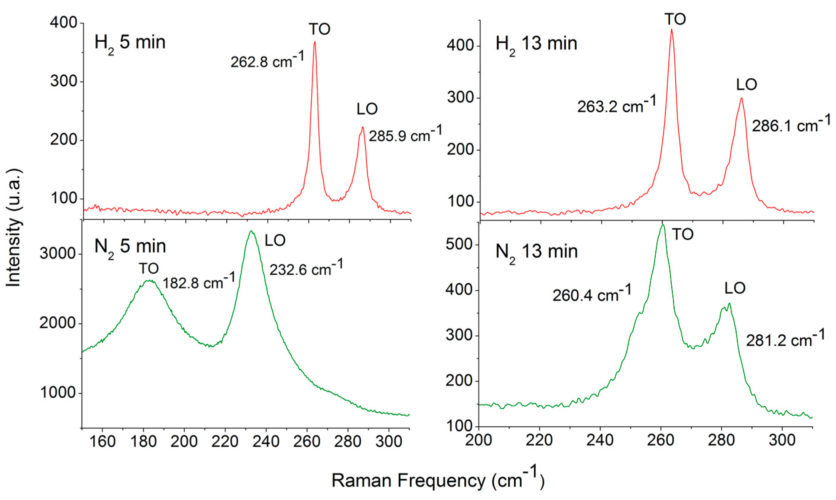
3.5. Micro-Raman Analysis
4. Conclusions
Author Contributions
Acknowledgments
Conflicts of Interest
References
- Adachi, S. Physical Properties of III-V Semiconductor Compounds; Wiley: Hoboken, NJ, USA, 1992. [Google Scholar]
- Moss, S.J.; Ledwith, A. The Chemistry of the Semiconductor Industry; Blackie: Houston, TX, USA, 1987. [Google Scholar]
- Scheel, H.J.; Fukuda, T. Crystal Growth Technology; Wiley: Hoboken, NJ, USA, 2003. [Google Scholar]
- Smart, L.; Elaine, E.; Moore, A. Solid State Chemistry: An Introduction; CRC Press: Boca Raton, FL, USA, 2012. [Google Scholar]
- Stringfellow, G.B. Organometallic Vapor-Phase Epitaxy: Theory and Practice; Academic Press: Cambridge, MA, USA, 1999. [Google Scholar]
- Cho, A.Y.; Arthur, J.R. Molecular beam epitaxy. Prog. Solid State Chem. 1975, 10, 157–191. [Google Scholar] [CrossRef]
- Gottlieb, G.E.; Corboy, J.F. Epitaxial growth og GaAs using water vapor. RCA Rev. 1963, 24, 585–595. [Google Scholar]
- Massé, G.; Lacroix, J.M.; Lawrence, M.F. Deep-level transient spectroscopy study of n-type GaAs epitaxial layers grown by close-spaced vapor transport. J. Appl. Phys. 1989, 65, 1126–1129. [Google Scholar] [CrossRef]
- Sagna, A.; Djessas, K.; Sene, C.; Medjnoun, K.; Grillo, S.E. Close spaced vapor transport deposition of Cu2ZnSnS4 thin films: Effect of iodine pressure. J. Alloys Compd. 2016, 685, 699–704. [Google Scholar] [CrossRef]
- Gómez-Barojas, E.; Silva-González, R.; Gracia-Jiménez, J.M.; Navarro-Contreras, H.; Vidal-Borbolla, M.A. Characterization of GaAs grown by the close-spaced vapor transport technique, using atomic hydrogen as the reactant. Phys. Status Solidi 2003, 198, 289–296. [Google Scholar] [CrossRef]
- Park, J.-H.; Sudarshan, T.S. Chemical Vapor Deposition; ASM International: Geauga County, OH, USA, 2001. [Google Scholar]
- Ritenour, A.J.; Boucher, J.W.; DeLancey, R.; Greenaway, A.L.; Aloni, S.; Boettcher, S.W. Doping and electronic properties of GaAs grown by close-spaced vapor transport from powder sources for scalable III–V photovoltaics. Energy Environ. Sci. 2015, 8, 278–285. [Google Scholar] [CrossRef]
- Silva-Andrade, F.; Ilinskii, A.; Chavez, F.; Prutskij, T.; Tenorio, F.; Bravo-Garcia, Y.; Pena-Sierra, R. Growth and Characterization of GaAs p-n Junctions Obtained by the CSVT Technique using Atomic Hydrogen. Mod. Phys. Lett. B 2001, 15, 752–755. [Google Scholar] [CrossRef]
- Hammadi, M.; Bourgoin, J.C.; Samic, H. Mechanism of GaAs transport by water reaction application to the growth of thick epitaxial layers. J. Mater. Sci. Mater. Electron. 1999, 10, 399–402. [Google Scholar] [CrossRef]
- Sun, G.C.; Zazoui, M.; Talbi, N.; Khirouni, K.; Bourgoin, J.C. Mobility-lifetime product in epitaxial GaAs X-ray detectors. Nucl. Instrum. Methods Phys. Res. Sect. A Accel. Spectrom. Detect. Assoc. Equip. 2007, 573, 228–231. [Google Scholar] [CrossRef]
- Kobayashi, R.; Fujii, K.; Hasegawa, F. Etching of GaAs by Atomic Hydrogen Generated by a Tungsten Filament. Jpn. J. Appl. Phys. 1991, 30, L1447–L1449. [Google Scholar] [CrossRef]
- Jung, M.; Eun, K.Y.; Lee, J.-K.; Baik, Y.-J.; Lee, K.-R.; Park, J.W. Growth of carbon nanotubes by chemical vapor deposition. Diam. Relat. Mater. 2001, 10, 1235–1240. [Google Scholar] [CrossRef]
- Parry, R.W.; Bassow, H.; Merrill, P. Chemistry, Experimental Foundations; Prentice-Hall: Upper Saddle River, NJ, USA, 1987. [Google Scholar]
- Wang, L.; Han, K.; Tao, M. Effect of Substrate Etching on Electrical Properties of Electrochemically Deposited CuO. J. Electrochem. Soc. 2007, 154, D91. [Google Scholar] [CrossRef]
- Pankove, J.I. Optical Processes in Semiconductors; Prentice Hall: Englewood Cliffs, NJ, USA, 1971. [Google Scholar]
- López, J.A.; López, J.C.; Valerdi, D.V.; Salgado, G.G.; Díaz-Becerril, T.; Pedraza, A.P.; Gracia, F.F. Morphological, compositional, structural, and optical properties of Si-nc embedded in SiOx films. Nanoscale Res. Lett. 2012, 7, 604. [Google Scholar] [CrossRef] [PubMed]
- Kayali, S.; Ponchak, G.; Shaw, R. GaAs MMIC Reliability Assurance Guideline forSpace Applications Preface. JPL Publ. 1996, 96, 58. [Google Scholar]
- Das, C.; Begum, J.; Begum, T.; Choudhury, S. Effect of thickness on the optical properties of Gaas thin films. J. Bangladesh Acad. Sci. 2013, 37, 83–91. [Google Scholar] [CrossRef]
- Cheong, H.M.; Zhang, Y.; Mascarenhas, A.; Geisz, J.F. Nitrogen-induced levels in GaAs 1 − x N x studied with resonant Raman scattering. Phys. Rev. B 2000, 61, 13687–13690. [Google Scholar] [CrossRef]
- Wei, S.-H.; Zunger, A. Giant and Composition-Dependent Optical Bowing Coefficient in GaAsN Alloys. Phys. Rev. Lett. 1996, 76, 664–667. [Google Scholar] [CrossRef] [PubMed]
- Bohr, S.; Haubner, R.; Lux, B. Influence of nitrogen additions on hot-filament chemical vapor deposition of diamond. Appl. Phys. Lett. 1996, 68, 1075–1077. [Google Scholar] [CrossRef]
- Foxon, C.T.; Harvey, J.A.; Joyce, B.A. The evaporation of GaAs under equilibrium and non-equilibrium conditions using a modulated beam technique. J. Phys. Chem. Solids 1973, 34, 1693–1701. [Google Scholar] [CrossRef]
- Vashista, M.; Paul, S. Correlation between full width at half maximum (FWHM) of XRD peak with residual stress on ground surfaces. Philos. Mag. 2012, 92, 4194–4204. [Google Scholar] [CrossRef]
- Pollak, F.H. Semiconductor Characterization by Raman Spectroscopy; Test and Measurements World: San Francisco, CA, USA, 1985. [Google Scholar]
- Tiong, K.K.; Amirtharaj, P.M.; Pollak, F.H.; Aspnes, D.E. Effects of As+ ion implantation on the Raman spectra of GaAs: ‘“Spatial correlation”’ interpretation. Appl. Phys. Lett. 1984, 44, 122–124. [Google Scholar] [CrossRef]
- Iikawa, F.; Cerdeira, F.; Vazquez-Lopez, C.; Motisuke, P.; Sacilotti, M.A.; Roth, A.P.; Masut, R.A. Raman Scattering from InGaAs/GaAs strained-layer superlattices. Solid State Commun. 1988, 68, 211–214. [Google Scholar] [CrossRef]
- Jain, S.C.; Willander, M.; Maes, H. Stresses and strains in epilayers, stripes and quantum structures of III-V compound semiconductors. Semicond. Sci. Technol. 1996, 11, 641–671. [Google Scholar] [CrossRef]
- Lannin, J.S.; Calleja, J.M.; Cardona, M. Second-order Raman scattering in the group-V semimetals: Bi, Sb, and As. Phys. Rev. B 1975, 12, 585–593. [Google Scholar] [CrossRef]


| Atmosphere | Deposition Time (min) | Thickness (µm) | Band Gap (eV) |
|---|---|---|---|
| H2 | 5 | 2.55 ± 0.035 | 1.861 ± 0.0018 |
| 13 | 12.99 ± 0.042 | 1.663 ± 0.0025 | |
| N2 | 5 | 1.04 ± 0.076 | 1.774 ± 0.0037 |
| 13 | 3.75 ± 0.058 | 1.644 ± 0.0033 |
| Atmosphere | Deposition Time (min) | at % | |||
|---|---|---|---|---|---|
| Ga | As | O | N | ||
| H2 | 5 | 53.49 ± 0.495 | 46.51 ± 0.480 | - | - |
| 13 | 50.59 ± 0.370 | 49.41 ± 1.091 | - | - | |
| N2 | 5 | 45.81 ± 0.355 | 32.70 ± 0.640 | 18.52 ± 0.575 | 2.98 ± 0.652 |
| 13 | 45.12 ± 0.545 | 41.02 ± 0.485 | 12.03 ± 0.540 | 1.83 ± 0.021 | |
| Atmosphere | Time (min) | Orientation | FWHM (degrees) | Crystallite Size (nm) | Phonon | FWHM (cm−1) | ||
|---|---|---|---|---|---|---|---|---|
| H2 | 5 | (111) | 0.055 ± 0.0012 | 147.384 ± 2.606 | TO | LO | 4.44 ± 0.119 | 6.45 ± 0.451 |
| H2 | 13 | (111) | 0.015 ± 0.0005 | 543.043 ± 14.749 | TO | LO | 4.98 ± 0.158 | 6.31 ± 0.369 |
| N2 | 5 | (111) | 0.329 ± 0.0043 | 24.801 ±0.264 | TO | LO | 15.81 ± 0.335 | 9.97 ± 0.678 |
| N2 | 13 | (111) | 0.121 ± 0.0035 | 67.502 ±1.594 | TO | LO | 19.08 ± 0.195 | 13.05 ± 0.444 |
© 2019 by the authors. Licensee MDPI, Basel, Switzerland. This article is an open access article distributed under the terms and conditions of the Creative Commons Attribution (CC BY) license (http://creativecommons.org/licenses/by/4.0/).
Share and Cite
Cruz Bueno, J.J.; García Salgado, G.; Balderas Valadez, R.F.; Luna López, J.A.; Nieto Caballero, F.G.; Díaz Becerril, T.; Rosendo Andrés, E.; Coyopol Solís, A.; Romano Trujillo, R.; Morales Ruiz, C.; et al. Effect of the Gaseous Atmosphere in GaAs Films Grown by Close-Spaced Vapor Transport Technique. Crystals 2019, 9, 68. https://doi.org/10.3390/cryst9020068
Cruz Bueno JJ, García Salgado G, Balderas Valadez RF, Luna López JA, Nieto Caballero FG, Díaz Becerril T, Rosendo Andrés E, Coyopol Solís A, Romano Trujillo R, Morales Ruiz C, et al. Effect of the Gaseous Atmosphere in GaAs Films Grown by Close-Spaced Vapor Transport Technique. Crystals. 2019; 9(2):68. https://doi.org/10.3390/cryst9020068
Chicago/Turabian StyleCruz Bueno, J. Jesús, Godofredo García Salgado, R. Fabiola Balderas Valadez, J. Alberto Luna López, F. Gabriela Nieto Caballero, Tomás Díaz Becerril, Enrique Rosendo Andrés, Antonio Coyopol Solís, Román Romano Trujillo, Crisóforo Morales Ruiz, and et al. 2019. "Effect of the Gaseous Atmosphere in GaAs Films Grown by Close-Spaced Vapor Transport Technique" Crystals 9, no. 2: 68. https://doi.org/10.3390/cryst9020068
APA StyleCruz Bueno, J. J., García Salgado, G., Balderas Valadez, R. F., Luna López, J. A., Nieto Caballero, F. G., Díaz Becerril, T., Rosendo Andrés, E., Coyopol Solís, A., Romano Trujillo, R., Morales Ruiz, C., Gracia Jiménez, J. M., & Galeazzi Isasmendi, R. (2019). Effect of the Gaseous Atmosphere in GaAs Films Grown by Close-Spaced Vapor Transport Technique. Crystals, 9(2), 68. https://doi.org/10.3390/cryst9020068