1. Introduction
The current interest in ZnO is mainly due to the optoelectronic properties of this wide bandgap semiconductor with potential applications in various devices [
1], such as light emitters [
2,
3] and UV photodetectors [
4]. An investigation of ZnO doped with copper is important as it presents additional information such as photocatalytic properties [
5] and ferromagnetic behavior [
6], making copper play an important role for potential applications in ZnO devices. Unlike other dopants, the similar ionic radius of copper compared to zinc allows its incorporation to take place with a reduced lattice distortion, resulting in a lower formation energy for the Cu on a substitutional site than on an interstitial site [
7]. In addition, the Cu has been demonstrated that it can behave as an acceptor in ZnO depending on its valence state [
8], and could be used to obtain p-type films, under certain conditions during deposition [
9,
10].
Investigation of the Cu diffusion in bulk ZnO single crystal is limited, and to the best of our knowledge there are only two reports of this [
11,
12] where the determination of the profile and diffusion coefficient has been obtained from optical absorption techniques. In this work, the profile and diffusion are studied by a more accurate method to quantify the concentration of impurities. In order to determine the Cu concentration incorporated by diffusion, to estimate the diffusion coefficient of Cu in ZnO at 1000 °C, and to establish the effect on conductivity and photoluminescent properties, we present the results of a secondary ion mass spectroscopy (SIMS) study of Cu diffusion in undoped n-type bulk ZnO (001) single crystal, their electrical characterization by the Hall effect, and the effect originated by Cu diffusion on the green emission studied by photoluminescence (PL) spectroscopy.
2. Materials and Methods
The samples used in this work were bulk ZnO (001) single crystals with dimensions of 5 mm × 5 mm, a thickness of 0.5 mm, and n-type conductivity with a polished surface purchased from MTI Co. (Richmond, CA, USA) and grown by the hydrothermal method. In order to reduce the H
2 interstitials [
13,
14] and to prepare the surface, the samples were annealed at 1050 °C in a dry air environment for one hour inside a quartz tube.
The source material was obtained from a Cu film (99.99% purity) with a thickness of 1 μm deposited by vacuum evaporation and then partially oxidized at 200 ° C for 30 minutes. After that, the diffusion was carried out under a N2 (99.999% purity) flow of 1 l/min for periods of 3, 6 and 15 hours inside a quartz tube furnace at 1000 °C. This temperature was chosen because around this point the diffusion process became more significant and the defect formation is lower than at higher temperatures. The analyses were performed after the removal of a residual copper oxide layer that remains after diffusion on the sample’s surface. The layer was removed with a soft polishing with alumina.
The diffusion profile of Cu in ZnO was determined by SIMS. Employing a mass spectrometer IMS-6f CAMECA (CAMECA instruments, Madison, WI, USA), the measurements were performed with a primary beam of 5 keV Cs+. The Hall effect measurements were carried out by applying a magnetic field of 0.37 T and a current of 1 mA. The PL measurements were performed at room temperature using a solid state violet laser (405 nm, 3.06 eV) with 60 mW, recording the spectrum intensity with a silicon photodetector through a half-meter monochromator.
3. Results
Figure 1 shows the concentration profiles obtained by SIMS for the three samples at different diffusion times. Observing an increase in the penetration depth of the Cu atoms as the diffusion time increases, the quantification of the Cu concentration at the surface is nearly the same with a value of approximately 2.5 × 10
19 cm
−3 Cu atoms, showing that the copper concentration is constant during the diffusion process. The appearing background of copper concentration in the zinc oxide samples of 4.3 × 10
17 cm
−3 is the result of the ion sputtering during the SIMS measurement process due to the use of undoped crystalline ZnO samples.
The solution for the Fick’s second law considering a dopant constant source case was fitted to experimental profiles adding a background value. The mathematical function for this case is proportional to an erfc function [
15] described by the following equation:
where
NCu(
x,
t) is the copper concentration diffused at a depth
x and a time
t,
N0 is the impurity constant concentration at the surface of the host material and
DCu is the copper diffusion coefficient for a specific temperature.
The normalized fitting for this equation to the experimental data is shown in
Figure 2. Solid lines are the best-fit curves for the solution equation, and this fit provides a Cu diffusion coefficient in ZnO at 1000 °C with a value of 2.42(±0.2) × 10
−12 cm
2∙s
−1. This value is consistent with those reported by Muller and Helbig [
11] with a value of 1.91(±1.1) × 10
−12 cm
2∙s
−1 since the obtained value is within the range of uncertainty expressed.
For the sample with a diffusion period of 15 hours, the experimental diffusion profile reveals a slight difference with the curve estimated from the solution equation, and as such presents a lower penetration than calculated by the solution function. This can be attributed to a possible change in the conditions or pathways for diffusion for greater diffusion times.
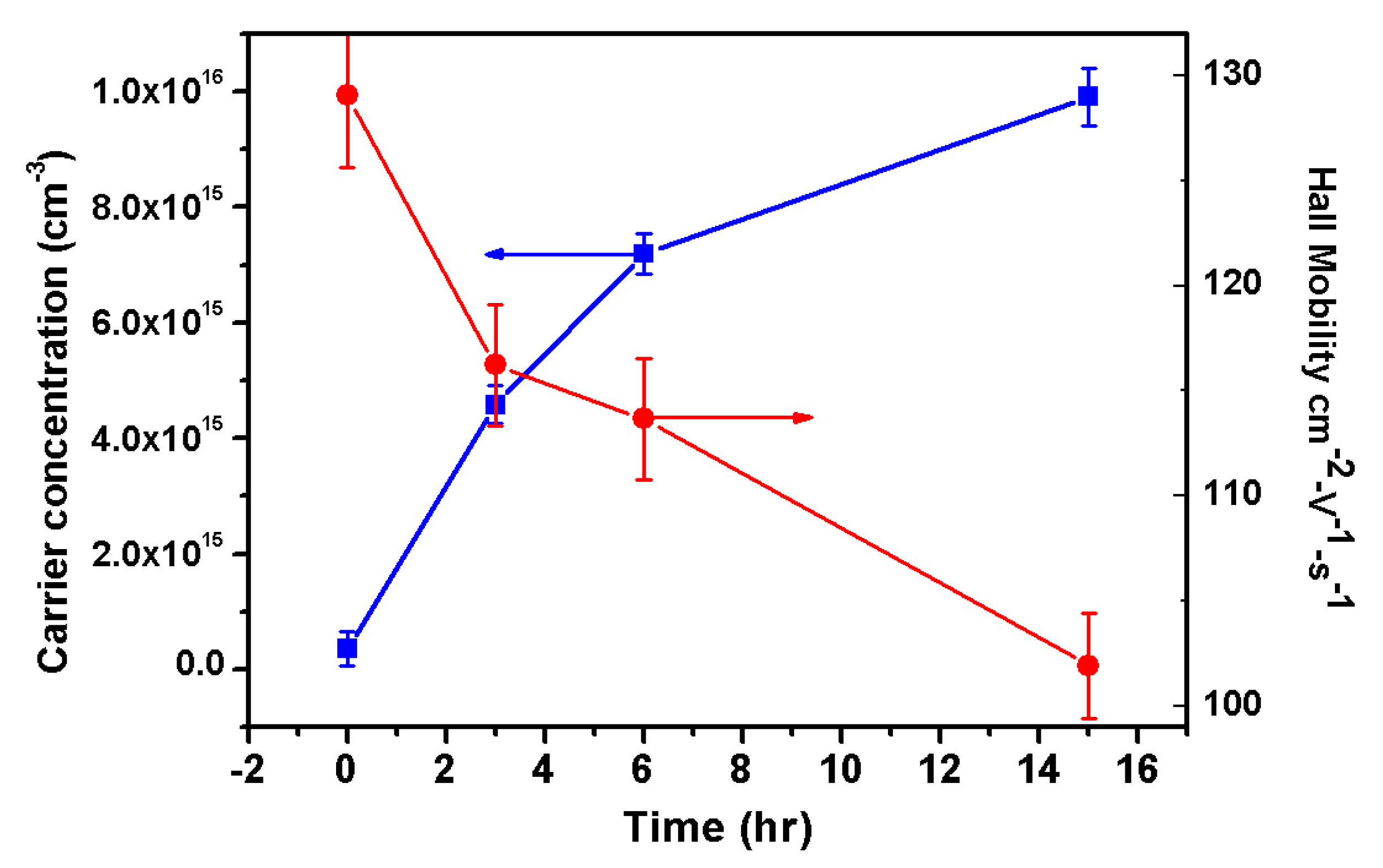
Electrical characterization was carried out by the Hall-Van der Pauw method, providing the carrier concentration and the electron mobility of the Cu diffused samples. The tendency observed on the measured characteristics are shown in
Figure 3 as a function of the diffusion time. The electron concentration increases in an order of magnitude with a slight decrement in the mobility.
The carrier concentration increases as the diffusion time was extended, but the electrical conductivity remains n-type with carrier mobility values relatively high. Since the carrier concentration is near to four orders of magnitude lower than Cu concentration determined by SIMS, this indicates that despite Cu atoms being introduced into ZnO, they are not acting as acceptors, and probably are not active. Hence the native donor defects dominate the electrical conductivity and the type. Further, a valence of copper as Cu
+ is decisive to obtain an acceptor behavior [
6] but this is not possible to identify by SIMS. On the other hand, the mobility is reduced with the diffusion time indicating that the material presents a change that affects the carrier scattering. In order to observe the electrical changes at the sample surface, the measured sheet resistance is presented in
Table 1, where a drastic change of resistance due to diffusion process is observed.
Figure 4 shows the PL spectra for the three ZnO samples with different copper diffusion times. It can be observed that the intensity of visible emissions centered on 2.35 eV increases with the diffusion time. This increment is attributed to a greater number of transitions between defects and copper, as already reported [
16]. The band edge emission is not observed because PL measurements were performed with a 405 nm (~3 eV) laser. However, the penetration of this laser is deeper, so the observed PL is not only from the surface but also the volume.
4. Discussion
The fitting of experimental data from three measured diffusion profiles to an erfc function using the same diffusion constant confirms that the diffusion of Cu in ZnO was carried out with a constant concentration at the surface and the atomic motion behaves according to Fick’s second law, as was reported by Herlotz [
12]. Deviation from the theoretical solution in the sample with the longer diffusion time can be attributed to a change of diffusion conditions at higher copper concentrations, such as new diffusion pathways or the formation of Cu complexes [
17]. The diffusion coefficient determined by SIMS in this work is consistent and slightly higher than reported by Muller [
11], probably due to the fact that optical absorption is an indirect method to quantify the copper concentration, whereas SIMS quantify the concentration through the detection of the copper mass and consequently achieves a higher accuracy.
The electrical characterization by the Hall effect reveals that despite the incorporation of Cu into ZnO the conductivity remains n-type. Observing an increase in the concentration as diffusion time is increased, this is attributed to the feasible donor defects generation by the process, and the fact that there are not enough dopants acting as acceptors in the suitable sites and valences. Differences between the Hall effect and the SIMS results are due to this last technique not detecting the sites neither the valence adopted by the Cu atoms in the lattice. The reduction of the carrier mobility could be produced by the incorporation of Cu, a likely formation of complexes, and the generation of defects by the process.
PL visible intensity was increased with the diffusion time. This is mostly due to the creation of electronic levels produced by the Cu incorporation in ZnO and/or the creation of defects by the diffusion process, since the visible emissions are typically associated to defects, and correlate with the electrical characterization that found a conductivity dominated by donors produced by intrinsic or extrinsic defects.

 ,
, 


