Communication

Baseline for Split DC Link Design in Three-Phase Three-Level Converters Operating with Unity Power Factor Based on Low-Frequency Partial Voltage Oscillations

1
School of Electrical and Computer Engineering, Ben-Gurion University of the Negev, Beersheba 84105, Israel
2
Department of Electrical and Electronics Engineering, Shamoon College of Engineering, Ashdod 8410802, Israel
*
Author to whom correspondence should be addressed.
Machines 2022, 10(9), 722; https://doi.org/10.3390/machines10090722
Submission received: 28 July 2022 / Revised: 21 August 2022 / Accepted: 22 August 2022 / Published: 24 August 2022
(This article belongs to the Special Issue Advances in High-Power Converters)

Abstract

:
The study sets a baseline for split DC link capacitance values and voltage set points in three-phase three-level AC/DC (or DC/AC) converters operating with unity power factor. In order to equalize the average values of partial DC link voltages, the controller generates a zero-sequence containing DC components only while employing neither dedicated DC link capacitance balancing hardware nor high-order zero-sequence component injection. Such a baseline is required in order to evaluate the effectiveness of different DC link capacitance reduction methods proposed in the literature. Unlike most previous works, utilizing neutral point current based on cumbersome analytical expressions to determine neutral point potential oscillations, the instantaneous power balance-based approach is employed in this paper, resulting in greatly simplified and more intuitive expressions. It is demonstrated that while the total DC link voltage is low-frequency ripple-free under unity power factor balanced AC-side operation, split DC link capacitors absorb triple-fundamental frequency power components with one-sixth load power magnitude. This yields significant opposite phase partial voltage ripples. In such a case, selection of DC link capacitances and voltage set points must take into account the expected values of AC-side phase voltage magnitude and split DC link capacitor voltage and current ratings. Simulation and experimental results validate the proposed methodology by application to a 10 kVA T-type converter prototype.

1. Introduction

Due to ever-increasing power demand of modern energy systems, the use of controlled high-power AC/DC and DC/AC converters has become more widespread [1]. Multilevel converters possess several important advantages over classical two-level converters such as better efficiency, lower dv/dt stress and better lower total harmonic distortion of the output voltage [2]. The most common topologies of multilevel converters are cascaded H-bridge, flying capacitor and neutral point clamped [3].
Multilevel converters are widely used in dual-stage power conversion systems with intermediate DC voltage link [4,5,6,7,8,9]. The DC link is typically realized by a single capacitor in the case of two-level conversion or multiple split capacitors in the case of multilevel conversion [10,11], providing power decoupling between the stages so that both converters can be controlled independently by various PWM methods [12,13,14,15,16,17,18]. Size, weight and price of DC link capacitors vary according to DC link voltage and power conversion system rating [19]. Furthermore, the lifetime of the capacitors is limited and it influences the reliability of the whole system [20]. Therefore, DC link voltages and capacitance values should be minimized [21,22,23].
Three-level three-phase AC/DC and DC/AC converters have been identified as the most viable topology for power ratings from 10–100 kVA and are widely used in industry [24]. Efficiency, reliability and output waveform quality of three-level converters are strongly dependent on the employed PWM method [25]. In case carrier-based PWM is applied, the main difference between the PWM methods is related to the zero-sequence voltage injection aimed to balance the split DC link capacitance voltages [26]. It should be emphasized that split capacitance balancing may be accomplished utilizing additional dedicated hardware [27,28], however, such a solution would increase system cost and physical size. On the other hand, different zero-sequence injection methods have been proposed over the years, allowing balancing of either average values of split DC link voltages in case of pure DC zero-sequence signal or instantaneous values of split DC link voltages in case the zero-sequence signal contains both DC and higher-order components [29,30,31,32,33]. Pure DC zero-sequence injection is the minimum required to sustain the DC link energy balance and is considered as the baseline in this paper. However, low-frequency neutral point voltage oscillations would appear under such an operation, requiring careful selection of both DC link capacitance values and corresponding voltage set points. Previous works evaluated the low-frequency neutral point voltage oscillations utilizing neutral point expression, which is quite cumbersome and cannot obtain an explicit analytical form [34,35]. Consequently, this paper proposes a methodology based on instantaneous split DC link powers rather than on neutral point current, allowing quantifying corresponding voltage oscillations analytically and intuitively. As a result, clear design guidelines are provided for split DC link capacitances and voltage set point values.
Since the paper focuses on low-frequency oscillations, switching frequency-related components are ignored for brevity in the presented discussion and may be adopted if needed from [35,36]. It is revealed that while the DC link voltage is low-frequency oscillation-free under unity power factor balanced AC-side operation, split DC link capacitors absorb triple-fundamental frequency one-sixth load magnitude powers, yielding opposite phase voltage oscillations. Consequently, selection of DC link capacitances and voltage set points must take into account the expected values of AC-side phase voltage magnitude and split DC link capacitor voltage and current ratings.
The outcomes of the proposed methodology may be used as a baseline for evaluation of advanced high-order zero-sequence injection algorithms, aimed to decrease low-frequency neutral point voltage oscillations and reduce the values of utilized split DC link capacitances. The presented findings’ validity is well-supported by simulations and experiments.

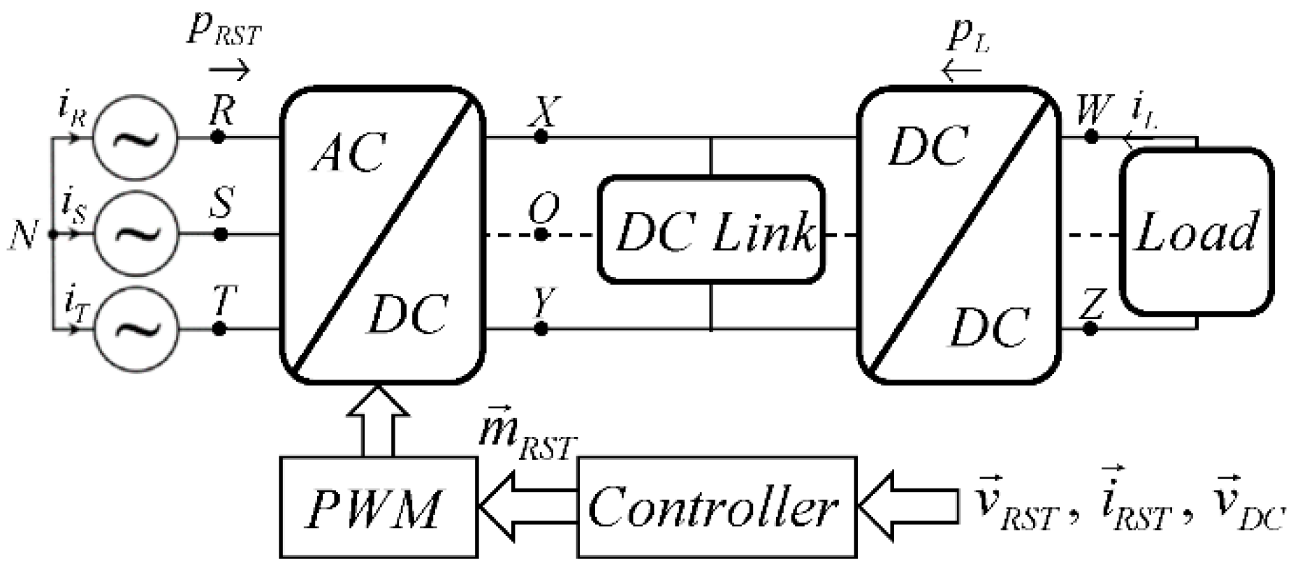
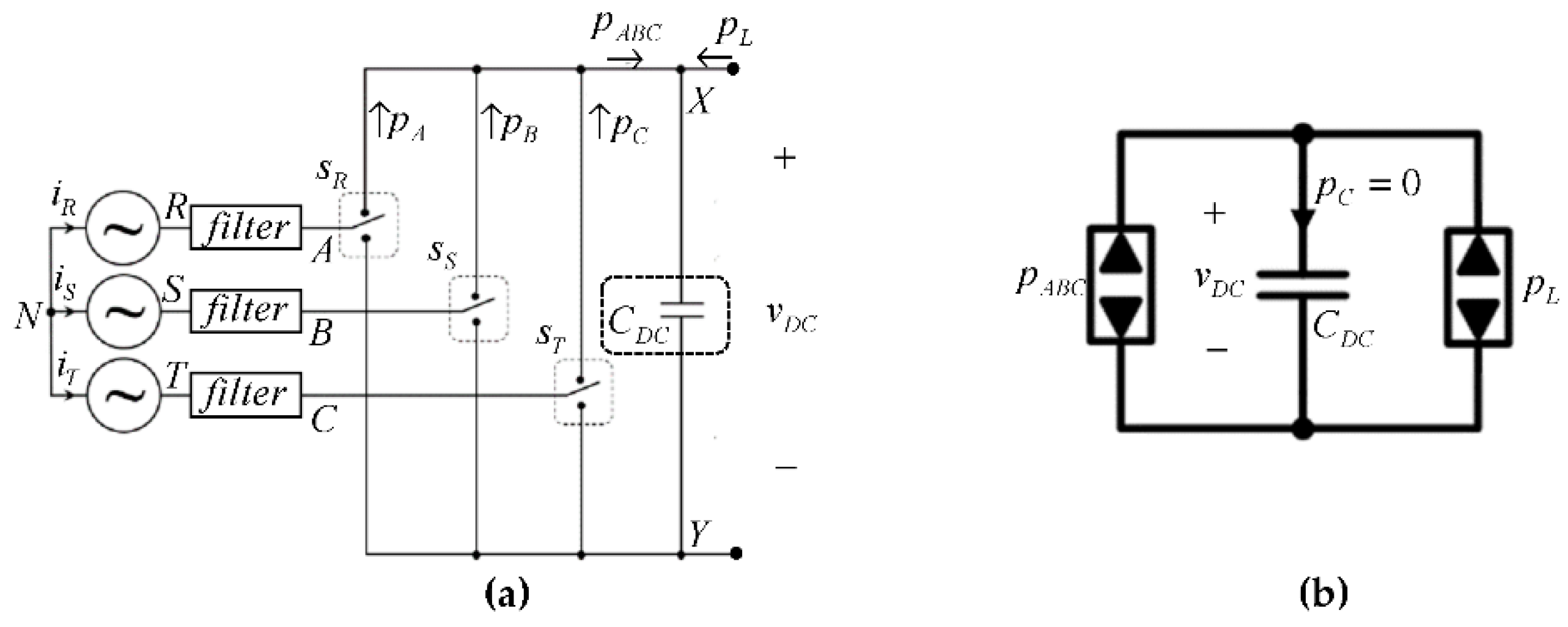
2. Materials and Methods
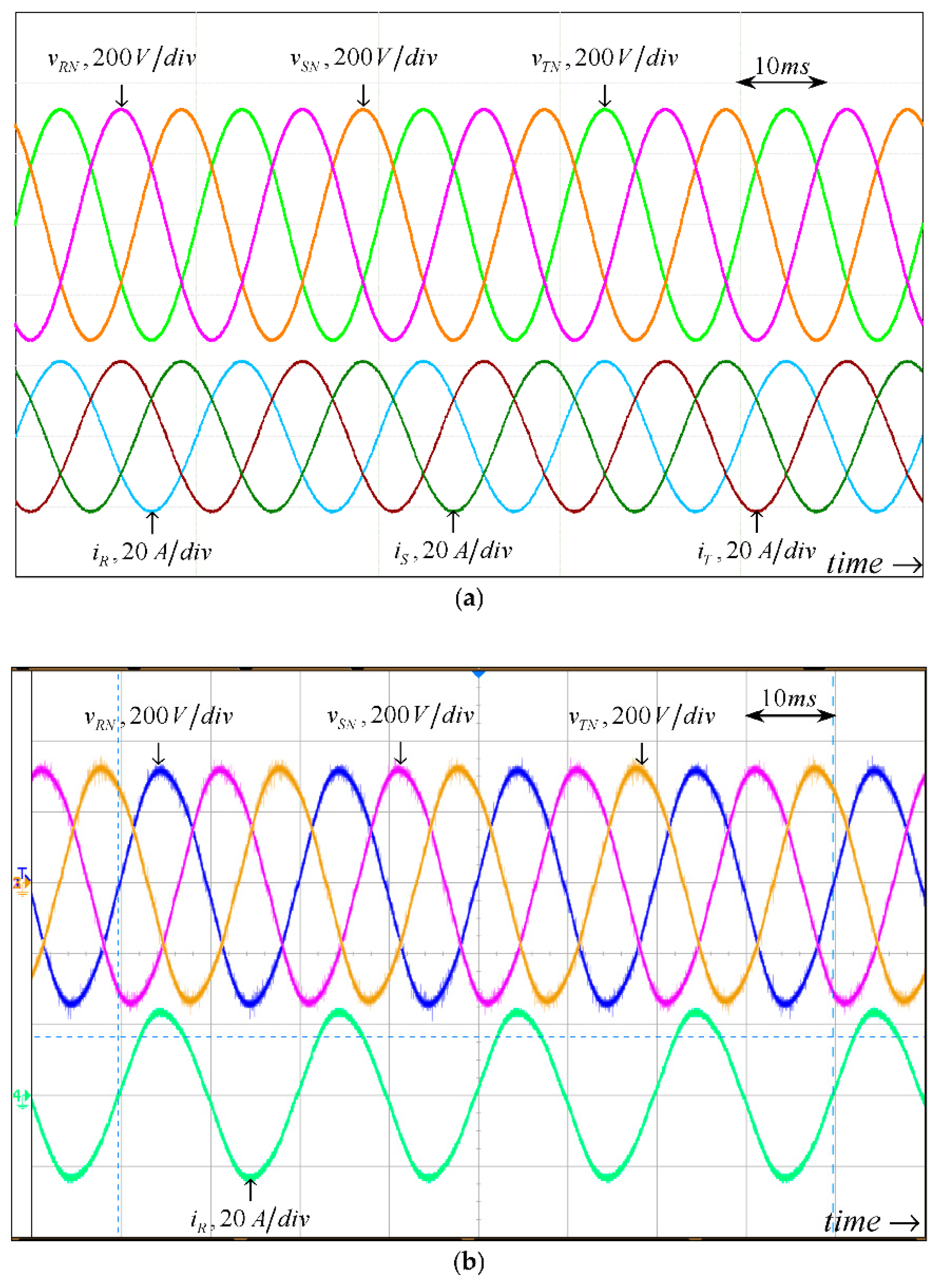
A typical three-phase power conversion system is depicted in Figure 1. The system consists of an AC/DC (or DC/AC) converter, DC link and DC/DC converter. It should be emphasized that the energy flow direction may be either from the AC- to DC-side or vice versa (i.e., “Load” in Figure 1 denotes a power source if the energy flows from the DC- to AC-side). Moreover, the DC link may be formed either by two terminals (X, Y) in case of two-level conversion or three terminals (X, O, Y) in case of three-level conversion. Upon balanced unity power factor operation, steady-state AC-side quantities (all the signals in the subsequent discussion are switching-cycle averaged) are given by
v R S T ( t ) = ( v R N ( t ) v S N ( t ) v T N ( t ) ) = V M ( sin ( ω t ) sin ( ω t φ ) sin ( ω t + φ ) ) i R S T ( t ) = ( i R ( t ) i S ( t ) i T ( t ) ) = I M ( sin ( ω t ) sin ( ω t φ ) sin ( ω t + φ ) )
with φ = 2 π / 3 , attained by applying pulse-width modulation signals of the form [29]
m R S T ( t ) = ( m R ( t ) m S ( t ) m T ( t ) ) M ( t ) ( sin ( ω t ) sin ( ω t φ ) sin ( ω t + φ ) ) + M 0 ( t ) .
The latter are created by the controller shown in Figure 1 with
v D C ( t ) = { v X Y ( t ) , 2 l e v e l c o n v e r t e r ( v X O ( t ) v Y O ( t ) ) 3 l e v e l c o n v e r t e r
and M(t), M0(t) denoting the modulation index and zero-sequence component, respectively. In case of two-level conversion, M0(t) in (2) is zero [33]. On the other hand, in the three-level conversion case, M0(t) contains the DC component only in the baseline design considered in this paper (allowing equalization of split DC link voltage average values), while in advanced designs it may contain both DC and high-order AC components (allowing equalization of split DC link voltage instantaneous values). It should be emphasized that M0(t) may also be supplied by an additional hardware-based equalization circuit [27,28].
Considering (1), the instantaneous AC-side phase power vector is given by
p R S T ( t ) = ( p R ( t ) p S ( t ) p T ( t ) ) = ( v R N ( t ) i R ( t ) v S N ( t ) i S ( t ) v T N ( t ) i T ( t ) ) = V M I M 2 ( 1 cos 2 ( ω t ) 1 cos 2 ( ω t φ ) 1 cos 2 ( ω t + φ ) ) ,
hence the total AC-side power is ripple free, given by
p R S T ( t ) = p R ( t ) + p S ( t ) + p S ( t ) = 3 2 V M I M = P R S T .
On the other hand, assuming DC-side voltage and current are governed by
v W Z ( t ) = V L ,       i L ( t ) = I L ,
The corresponding steady-state instantaneous power is also constant, given by
p L ( t ) = v W Z ( t ) i L ( t ) = V L I L = P L .
Consequently, the instantaneous system power balance (neglecting conversion losses and energy stored in AC-side L-, LC- or LCL-type filters [37]) is given by
P R S T = 3 2 V M I M = V L I L = P L ,
indicating that the instantaneous low-frequency DC link power is zero. In case a converter belongs to the generalized two-level three-phase topology in Figure 2a, its DC link is formed by a single capacitor CDC. Since M0(t) = 0, total switching cycle averaged power at the converter AC-side pABC(t) is equal to pRST(t). Hence, pC(t) = 0 (cf. Figure 2b) and vDC(t) is low-frequency ripple free and regulated to a predefined DC link voltage set point V D C * . On the other hand, in case of a converter belonging to the generalized three-level three-phase topology in Figure 3a, split capacitor pair CDC1, CDC2 forms the DC link. According to the above, pC(t) = pC1(t) + pC2(t) = 0 and hence vDC(t) is still low-frequency ripple free, yet without implying zero pC1(t), pC2(t) and low-frequency ripple free vDC1(t), vDC2(t), as shown next. Note that the line connecting the middle point of the DC link with the load middle point is virtual and may be nonexistent in reality. It is only used to demonstrate that the power element pL may be split into two halves [38].
Since AC-side voltages v R S T ( t ) and currents i R S T ( t ) in Figure 3 cannot contain zero-sequence components (even for nonzero M0(t)), corresponding power vectors are still given by (4). On the other hand, converter AC-side voltages v A B C ( t ) = ( v A N ( t ) v B N ( t ) v C N ( t ) ) T would contain DC components in case corresponding modulation signals are DC-shifted, yielding (cf. Figure 3b)
p A 1 B 1 C 1 ( t ) = { ( v A N ( t ) i R ( t ) v B N ( t ) i S ( t ) v C N ( t ) i T ( t ) ) , i A B C ( t ) > 0 0 , i A B C < 0 = ( p A 1 ( t ) + P 0 3 p B 1 ( t ) + P 0 3 p C 1 ( t ) + P 0 3 ) p A 2 B 2 C 2 ( t ) = { 0 , i A B C ( t ) > 0 ( v A N ( t ) i R ( t ) v B N ( t ) i S ( t ) v C N ( t ) i T ( t ) ) , i A B C < 0 = ( p A 2 ( t ) P 0 3 p B 2 ( t ) P 0 3 p C 2 ( t ) P 0 3 )
with P0/3 denoting the DC power component imposed by M0. Hence, partial converter AC-side low-frequency powers exchanged with the DC link (neglecting conversion losses and energy stored in AC-side filters) are given by
p A B C 1 ( t ) = p A 1 ( t ) + p B 1 ( t ) + p C 1 ( t ) P L 2 + P 0 + P L 6 sin ( 3 ω t ) p A B C 2 ( t ) = p A 2 ( t ) + p B 2 ( t ) + p C 2 ( t ) P L 2 P 0 P L 6 sin ( 3 ω t ) .
Note that P0 may be either positive or negative, allowing compensating instantaneous energy shortage of any split DC link capacitors. In case of load power mismatch ΔpL (cf. Figure 3b), instantaneous system power balance (8) is sustained with P0 = ΔpL and partial low-frequency DC link powers are given in steady state by
p C 1 ( t ) = v D C 1 ( t ) C D C 1 d v D C 1 ( t ) d t P L 6 sin ( 3 ω t ) p C 2 ( t ) = v D C 2 ( t ) C D C 2 d v D C 2 ( t ) d t P L 6 sin ( 3 ω t ) .
According to (11), each of the split DC link capacitors absorbs triple-fundamental frequency power component with one-sixth load power magnitude. In case partial capacitor voltages are regulated to set points given by V D C 1 * and V D C 2 * , respectively, corresponding instantaneous low-frequency energies and steady-state voltages would be
e D C 1 ( t ) C D C 1 2 ( V D C 1 * ) 2 P L 18 ω cos ( 3 ω t ) = C D C 1 2 v D C 1 2 ( t ) e D C 2 ( t ) C D C 2 2 ( V D C 2 * ) 2 + P L 18 ω cos ( 3 ω t ) = C D C 2 2 v D C 2 2 ( t ) v D C 1 ( t ) = V D C 1 * 1 P L 9 ω ( V D C 1 * ) 2 C D C 1 cos ( 3 ω t ) v D C 2 ( t ) = V D C 2 * 1 + P L 9 ω ( V D C 2 * ) 2 C D C 2 cos ( 3 ω t ) ,
respectively. Typically,
V D C 1 * = V D C 2 * = 0.5 V D C * , C D C 1 = C D C 2 = C D C
are employed, therefore (12) reduces to
v D C 1 , 2 ( t ) = 0.5 V D C * 1 ± P L 9 ω ( 0.5 V D C * ) 2 C D C cos ( 3 ω t ) 0.5 V D C * ± P L 9 ω V D C * C D C Δ V D C 1 , 2 cos ( 3 ω t ) ,
i.e., split capacitor voltages contain DC components as well as nonzero opposite phase triple-fundamental frequency ripples. The approximation in (14) is valid in practical systems where the low-frequency DC link voltage ripple magnitude ΔVDC1,2 is much lower than the corresponding voltage set point V D C 1 * , V D C 2 * [39]. Low-frequency split capacitor currents and corresponding RMS values are then obtained as
i D C 1 , 2 3 ω ( t ) = C D C d v D C 1 , 2 ( t ) d t = P L 3 V D C * sin ( 3 ω t ) R M S ( i D C 1 , 2 3 ω ) = P L 3 2 V D C * .
If split DC link capacitors possess significant equivalent series resistance RC, then (14) becomes
v D C 1 , 2 ( t ) 0.5 V D C * ± P L 9 ω V D C * C D C cos ( 3 ω t ) R C P L 3 V D C * sin ( 3 ω t )
and the low-frequency DC link ripple magnitude is given by
Δ V D C 1 , 2 P L V D C * ( 1 9 ω C D C ) 2 + ( R C 3 ) 2 .
Instantaneous partial DC link voltages are typically bounded as
V M I N < v D C 1 , 2 ( t ) < V M A X ,
where VMAX is imposed by capacitor (or switching devices) voltage rating and VMIN is dictated by the magnitude of AC-side phase voltages. Combining (18) with (16) yields the required capacitance value, given by
C D C > 1 9 ω min { ( V D C * P L ( V M A X 0.5 V D C * ) ) 2 ( R C 3 ) 2 , ( V D C * P L ( 0.5 V D C * V M I N ) ) 2 ( R C 3 ) 2 } .
In order to decrease the DC link capacitance values by utilizing the whole allowable DC link voltage span, DC link voltage set point should be set to [40]
V D C * = 2 ( V M A X 2 + V M I N 2 ) ,
yielding
C D C > 1 9 ω ( V D C * P L ( V M A X V M A X 2 + V M I N 2 2 ) ) 2 ( R C 3 ) 2 .
Nevertheless, one must recall that according to (15), increasing the DC link voltage set point decreases the RMS value of low-frequency split capacitor currents, and vice versa. If the allowed RMS value of low-frequency split capacitor current is bounded by IRMS,MAX, DC link voltage set point must obey
V D C * P L 3 2 I R M S , M A X .

3. Validation

In order to validate the revealed methodology, consider a 10 kVA LCL filter-based three-phase three-level T-type converter, depicted in Figure 4a. The corresponding experimental prototype is shown in Figure 4b, constructed according to design guidelines given in [41]. The converter was operated at 50 kHz switching frequency by Texas Instruments TMS320F28335 DSP. The power stage was fed by a DC power supply and terminated by a three-phase balanced resistive load, drawing nominal power for phase voltage magnitude of VM = 230 2 V ≈ 325 V. The power stage was operated semi-open loop by applying pulse-width modulation signals (2) with M(t) = 325/(0.5∙ V D C * ) (open loop) and M0(t) determined as shown in Figure 5 with NF150 representing a 150 Hz centered notch filter aimed to remove the triple-mains-frequency ripple so that the zero-sequence component contains DC constituent only, as desired, and K0 denoting a constant gain (closed loop). Simulated (PSIM software) and experimental AC-side variables are depicted in Figure 6 (only one phase current is shown experimentally due to 4-channel oscilloscope usage). It is well-evident that the system operates with unity power factor under rated loading.
A.
Capacitor low-frequency current rating imposed design
Consider DC link capacitors with low-frequency current rating of 3 ARMS. Then, according to (22),
V D C * > P L 9 2 = 786 V V D C 1 , 2 * > 393 V
must be selected. In case the capacitors are 450 V rated, the corresponding maximum value of the DC link voltage should remain below 410 V (i.e., keeping a 10% margin) to prolong the capacitors’ lifetime [42]. Setting V D C * to 790 V (i.e., V D C 1 * and V D C 2 * to 395 V) and assuming RC = 0.5 Ω (cf. (19)), the required DC link capacitance of CDC > 458 μF is imposed. Four parallel connected 110 μF capacitors were employed for validation. The corresponding results are shown in Figure 7. It is well-evident that the maximum value of partial DC link voltages corresponds well to the upper bound constraint. On the other hand, the minimum value of partial DC link voltages is much higher than AC-side voltage magnitude. Experimental results possess a slightly higher switching ripple due to inductive component of practical capacitors, yet the average value of the partial low-frequency DC link voltage ripple magnitude (both simulated and experimental) is about ~10 V, matching analytical prediction in (17) well.
B.
Capacitor voltage rating imposed design
Next, consider the availability of DC link capacitors with voltage rating of 400 V. Then, the corresponding maximum value of the DC link voltage should remain below 360 V (again, considering a 10% margin for capacitor lifetime elongation). On the other hand, the minimum DC link voltage value should remain above VM (330 V is selected to allow a safety margin of 5 V). According to (20), in order to utilize the whole allowable DC link voltage span, DC link voltage set point V D C * should be selected as 695 V (i.e., V D C 1 * and V D C 2 * set to 347.5 V). Assuming RC = 0.5 Ω, DC link capacitance of CDC > 433 μF is required according to (21). Again, four parallel connected 110 μF capacitors were employed for validation. The corresponding results are shown in Figure 8. It is well-evident that both the maximum and minimum values of partial DC link voltages correspond well to the upper and lower bound constraints. Once more, experimental results possess a slightly higher switching ripple due to nonideal capacitor usage, yet the average value of the partial low-frequency DC link voltage ripple magnitude (both simulated and experimental) is about ~12 V, matching analytical prediction in (17) well. Compared to the previous experiment, it may be concluded that the ripple has increased due to decreased V D C * , as expected.

4. Conclusions

Design guidelines for split DC link capacitors and corresponding voltage set point value selection for three-phase three-level converters were established in the paper for the baseline case in which only average values of partial DC link voltages are equalized. It was shown that operational restrictions are imposed by the fact that even though the DC link voltage is low-frequency ripple free, partial voltages possess significant anti-phase triple-fundamental-frequency ripples. The proposed methodology utilized instantaneous power balance expressions to obtain simple and intuitive analytical expressions for partial DC link voltage oscillation quantification. Simulations and experiments carried out by applying the proposed methodology to a 10 kVA T-type converter successfully validated the revealed findings.

Author Contributions

Conceptualization, D.B. and A.K.; methodology, Y.S. and A.K.; software, V.Y.; validation, Y.S. and V.Y.; formal analysis, A.K.; investigation, Y.S.; resources, A.K.; data curation, Y.S. and V.Y.; writing—original draft preparation, D.B.; writing—review and editing, A.K.; visualization, Y.S. and V.Y.; supervision, D.B. and A.K.; project administration, A.K.; funding acquisition, A.K. All authors have read and agreed to the published version of the manuscript.

Funding

This research was funded by the Israel Science Foundation under grant 2186/19, and by the Israel Ministry of Energy.

Data Availability Statement

Not applicable.

Conflicts of Interest

The authors declare no conflict of interest.

References

  1. Bose, B.K. Multi-Level Converters. Electronics 2015, 4, 582–585. [Google Scholar] [CrossRef]
  2. Franquelo, L.G.; Leonand, J.; Rodriguez, J. The age of multilevel converters arrives. IEEE Ind. Electron. Mag. 2008, 2, 28–39. [Google Scholar] [CrossRef] [Green Version]
  3. Rodriguez, J.; Lai, J.-S.; Peng, F.Z. Multilevel inverters: A survey of topologies, controls, and applications. IEEE Trans. Ind. Electron. 2002, 49, 724–738. [Google Scholar] [CrossRef] [Green Version]
  4. Norões, M.; Jacobina, C.B.; Carlos, G.A. A new three-phase ac–dc–ac multilevel converter based on cascaded three-leg converters. IEEE Trans. Ind. Appl. 2017, 53, 2210–2221. [Google Scholar]
  5. Zhou, D.; Zhao, J.; Li, Y. Model-predictive control scheme of five-leg ac–dc–ac converter-fed induction motor drive. IEEE Trans. Ind. Electron. 2016, 63, 4517–4526. [Google Scholar] [CrossRef]
  6. Lima, M.; Cursino, B.J.; Rocha, N.; Santos, E.C. Ac–dc–ac three-phase converter based on three three-leg converters connected in series. IEEE Trans. Ind. Appl. 2016, 52, 3171–3181. [Google Scholar]
  7. Filho, S.; Cipriano, O.; de Almeida, B.R.; Souza, D.; Neto, T.R.F. High-frequency isolated AC–DC–AC interleaved converter for power quality applications. IEEE Trans. Ind. Appl. 2018, 54, 4594–4602. [Google Scholar] [CrossRef]
  8. Norões, M.; Jacobina, C.B.; Freitas, N.B.; Queiroz, A.; Silva, E.R.C. Three-phase four-wire ac–dc–ac multilevel topologies obtained from an interconnection of three-leg converters. IEEE Trans. Ind. Appl. 2018, 54, 4728–4738. [Google Scholar]
  9. Norões, M.; Jacobina, C.B.; Freitas, N.B.; Alves Vitorino, M. Investigation of three-phase ac–dc–ac multilevel nine-leg converter. IEEE Trans. Ind. Appl. 2016, 52, 4156–4169. [Google Scholar]
  10. Kaufhold, E.; Meyer, J.; Schegner, P. Measurement-based identification of DC-link capacitance of single-phase power electronic devices for grey-box modelling. IEEE Trans. Power Electron. 2021, 37, 4545–4552. [Google Scholar] [CrossRef]
  11. Khalil, A.; Ahmed, G.; Lee, D.C. DC-link capacitance estimation in AC/DC/AC PWM converters using voltage injection. IEEE Trans. Ind. Appl. 2008, 44, 1631–1637. [Google Scholar] [CrossRef]
  12. Divan, D.; Habetler, T.; Lipo, T. PWM techniques for voltage source inverters. In Proceedings of the IEEE Power Electronics Specialists Conference, Charleston, SC, USA, 1 July 1999. [Google Scholar]
  13. Laszlo, H.; Kumar, M.; Jovanović, M.M. Performance comparison of three-step and six-step PWM in average-current-controlled three-phase six-switch boost PFC rectifier. IEEE Trans. Power. Electron. 2016, 31, 7264–7272. [Google Scholar]
  14. Lu, Y.; Zhao, Z.; Lu, T.; Yang, S.; Zou, G. An improved DC-link voltage fast control scheme for a PWM rectifier-inverter system. IEEE Trans. Ind. Appl. 2014, 50, 462–473. [Google Scholar]
  15. Xiong, X.; Zhang, Y.; Wang, J.; Du, H. An improved model predictive control scheme for the PWM rectifier-inverter system based on power-balancing mechanism. IEEE Trans. Ind. Electron. 2016, 63, 5197–5208. [Google Scholar]
  16. Sahraoui, K.; Gaoui, B. Reconfigurable control of PWM AC-DC-DC converter without redundancy leg supplying an ac motor drive. Period. Polytech. Electr. Eng. Comp. Sci. 2021, 65, 74–81. [Google Scholar] [CrossRef]
  17. Sitbon, M.; Leppaaho, J.; Suntio, T.; Kuperman, A. Dynamics of photovoltaic-generator-interfacing voltage-controlled buck power stage. IEEE J. Photovolt. 2014, 5, 633–640. [Google Scholar] [CrossRef]
  18. Iqbal, A.; Lewicki, A.; Morawiec, M. Pulse-width modulation of power electronic DC–AC converter. In High Performance Control of AC Drives with MATLAB®/Simulink, 2nd ed.; Wiley: Hoboken, NJ, USA, 2021. [Google Scholar]
  19. Pu, X.-S.; Nguyen, T.H.; Lee, D.-C.; Lee, K.-B.; Kim, J.-M. Fault diagnosis of DC-link capacitors in three-phase AC/DC PWM converters by online estimation of equivalent series resistance. IEEE Trans. Ind. Electron. 2013, 60, 4118–4127. [Google Scholar] [CrossRef]
  20. Pu, X.-S.; Nguyen, T.H.; Lee, D.-C.; Lee, S.-G. Identification of DC-link capacitance for single-phase AC/DC PWM converters. J. Pow. Electron. 2010, 10, 270–276. [Google Scholar] [CrossRef] [Green Version]
  21. Hur, N.; Jung, J.; Nam, K. A fast dynamic DC-link power-balancing scheme for a PWM converter-inverter system. IEEE Trans. Ind. Electron. 2001, 48, 794–803. [Google Scholar]
  22. Gu, B.-G.; Nam, K. A DC-link capacitor minimization method through direct capacitor current control. IEEE Trans. Ind. Appl. 2006, 42, 573–581. [Google Scholar]
  23. Malesani, L.; Rossetto, L.; Tenti, P.; Tomasin, P. AC/DC/AC PWM converter with reduced energy storage in the DC link. IEEE Trans. Ind. Appl. 1995, 31, 287–292. [Google Scholar] [CrossRef] [Green Version]
  24. Stecca, M.; Soeiro, T.B.; Elizondo, L.R.; Bauer, P.; Palensky, P. Comparison of two and three-level DC-AC converters for a 100 kW battery energy storage system. In Proceedings of the IEEE International Symposium on Industrial Electronics, Delft, The Netherlands, 17–19 June 2020; pp. 677–682. [Google Scholar]
  25. Novak, M.; Sangwongwanich, A.; Blaabjerg, F. Online optimization of zero-sequence voltage injection of PWM strategy for 3L-NPC converters. In Proceedings of the IEEE International Power Electronics Conference, Himeji, Japan, 15–19 May 2022; pp. 2405–2411. [Google Scholar]
  26. Sangwongwanich, A.; Novak, M.; Sangwongwanich, S.; Blaabjerg, F. Reliability of DC-link capacitors in three-level NPC inverters under different PWM methods. In Proceedings of the IEEE Applied Power Electronics Conference and Exposition, Houston, TX, USA, 20–24 March 2022; pp. 1804–1811. [Google Scholar]
  27. In, H.-C.; Kim, S.-M.; Lee, K.-B. Design and control of small DC-link capacitor-based three-level inverter with neutral-point voltage balancing. Energies 2018, 11, 1435. [Google Scholar] [CrossRef] [Green Version]
  28. Zielinski, C.; Stefanczak, B.; Jedrus, K. Phase-independent reactive power compensation based on four-wire power converter in the presence of angular asymmetry between voltage vectors. Energies 2022, 15, 497. [Google Scholar] [CrossRef]
  29. Cao, D.P.; Song, W.X.; Xi, H.; Chen, G.C.; Chen, C. Research on zero-sequence signal of space-vector modulation for three-level neutral-point-clamped inverter based on vector diagram partition. In Proceedings of the 6th IEEE International Power Electronics and Motion Control Conference, Wuhan, China, 17–20 May 2009; pp. 1435–1439. [Google Scholar]
  30. Helle, L.; Munk-Nielsen, S.; Enjeti, P. Generalized discontinuous DC-link balancing modulation strategy for three-level inverters. In Proceedings of the Power Conversion Conference, Osaka, Japan, 2–5 April 2002; pp. 359–366. [Google Scholar]
  31. Song, Q.; Liu, W.; Yu, Q.; Xie, X.; Wang, Z. A neutral-point potential balancing algorithm for three-level NPC inverters using analytically injected zero-sequence voltage. In Proceedings of the IEEE. Applied Power Electronics Conference and Exposition, Miami Beach, FL, USA, 9–13 February 2003; pp. 228–233. [Google Scholar]
  32. Pou, J.; Zaragoza, J.; Rodriguez, P.; Ceballos, S.; Sala, V.M.; Burgos, R.P.; Boroyevich, D. Fast-processing modulation strategy for the neutral-point-clamped converter with total elimination of low-frequency voltage oscillations in the neutral point. IEEE Trans. Ind. Electron. 2007, 54, 2288–2294. [Google Scholar] [CrossRef]
  33. Alemi, P.; Jeung, Y.-C.; Lee, D.-C. DC-link capacitance minimization in T-type three-level AC/DC/AC PWM converters. IEEE Trans. Ind. Electron. 2015, 62, 1382–1391. [Google Scholar] [CrossRef]
  34. Pou, J.; Pindado, R.; Boroyevich, D.; Rodriguez, P. Evaluation of the low-frequency neutral-point voltage oscillations in the three-level inverter. IEEE Trans. Ind. Electron. 2005, 52, 1582–1588. [Google Scholar] [CrossRef]
  35. Gopalakrishnan, K.S.; Janakiraman, S.; Das, S.; Narayanan, G. Analytical evaluation of DC capacitor RMS current and voltage ripple in neutral-point clamped inverters. Sadhana 2017, 42, 827–839. [Google Scholar] [CrossRef] [Green Version]
  36. Orfanoudakis, G.I.; Yuratich, M.A.; Sharkh, S.M. Analysis of dc-link capacitor current in three-level neutral point clamped and cascaded H-bridge inverters. IET Pow. Electron. 2013, 6, 1376–1389. [Google Scholar] [CrossRef]
  37. Beres, R.N.; Wang, X.; Liserre, M.; Blaabjerg, F.; Bak, C.L. A review of passive power filters for three-phase grid-connected voltage-source converters. IEEE J. Emerg. Sel. Top. Pow. Electron. 2016, 4, 54–69. [Google Scholar] [CrossRef] [Green Version]
  38. Singer, S.; Erickson, R.W. Power-source element and its properties. IEEE Proc. Circ. Dev. Syst. 1994, 141, 220–226. [Google Scholar] [CrossRef]
  39. Mellinkovsky, M.; Yuhimenko, V.; Zhong, Q.C.; Peretz, M.M.; Kuperman, A. Active DC link capacitance reduction in grid-connected power conversion systems by direct voltage regulation. IEEE Access 2018, 6, 18163–18173. [Google Scholar] [CrossRef]
  40. Mutovkin, A.; Yuhimenko, V.; Mellinkovsky, M.; Schacham, S.; Kuperman, A. Control of direct voltage regulated active DC-link capacitance reduction circuits to allow plug-and-play operation. IEEE Trans. Ind. Electron. 2019, 66, 6527–6537. [Google Scholar] [CrossRef]
  41. Available online: https://www.ti.com/lit/ug/tidue53f/tidue53f.pdf (accessed on 28 July 2022).
  42. Available online: https://product.tdk.com/system/files/dam/doc/product/capacitor/aluminum-electrolytic/snap-in/data_sheet/20/30/db/aec/b43643.pdf (accessed on 28 July 2022).
Figure 1. Generalized dual-stage power conversion system.
Machines 10 00722 g001
Figure 2. Two-level three-phase power conversion topology. (a) Generalized circuitry. (b) Power-level equivalent circuit of the DC link.
Machines 10 00722 g002
Figure 3. Three-level three-phase power conversion topology. (a) Generalized circuitry. (b) Power-level equivalent circuit of the DC link.
Machines 10 00722 g003
Figure 4. T-type three-phase three-level power converter. (a) Power stage circuitry. (b) The 10 KVA experimental prototype.
Machines 10 00722 g004
Figure 5. Generation of zero-sequence component M0(t).
Machines 10 00722 g005
Figure 6. AC-side nominal loaded converter voltages and currents. (a) Simulation. (b) Experiment.
Machines 10 00722 g006
Figure 7. Results of capacitor low-frequency current rating imposed design. (a) Simulation. (b) Experiment.
Machines 10 00722 g007
Figure 8. Results of capacitor voltage rating imposed design. (a) Simulation. (b) Experiment.
Machines 10 00722 g008
Publisher’s Note: MDPI stays neutral with regard to jurisdictional claims in published maps and institutional affiliations.

