Article

Improved Current-Sharing Imbalance Control Model Based on Magnetic Ferrite Inductance and a Gate Drive Circuit

1
Tianjin Key Laboratory of Optoelectronic Detection Technology and Systems, School of Electronic and Information Engineering, Tiangong University, Tianjin 300387, China
2
Engineering Research Center of High Power Solid State Lighting Application System of Ministry of Education, Tiangong University, Tianjin 300387, China
3
Key Laboratory of Smart Grid of Ministry of Education, School of Electrical and Information Engineering, Tianjin University, Tianjin 300072, China
4
School of Physical Science and Technology, Tiangong University, Tianjin 300387, China
*
Author to whom correspondence should be addressed.
Machines 2023, 11(2), 197; https://doi.org/10.3390/machines11020197
Submission received: 28 December 2022 / Revised: 25 January 2023 / Accepted: 30 January 2023 / Published: 1 February 2023
(This article belongs to the Section Automation and Control Systems)

Abstract

:
The dynamic and static imbalance of parallel current sharing has held the concern of researchers in view of the variation in multiple parasitic parameters on high-frequency parallel switching mode power supply (SMPS). The joint simulations and suppression experiments on the parallel current-sharing imbalance of various parasitic parameters are investigated on the improved dual-pulse detection circuit platform to determine the method of detecting the parallel current-sharing imbalance ratio using the sum of the differential magnetic flux. An improved model of current-sharing imbalance control is presented consisting of magnetic ferrite inductance and a gate drive circuit. The main concerns are the suppression performance of drain, gate, and source parasitic inductance, gate–source capacitance, driving time and voltage, gate resistance, and delayed forward/reverse driving signals on the ratio of parallel current-sharing imbalance, respectively. The improved model effectively reduces the parallel current-sharing imbalance ratio by more than 5% and 2–4.2%, compared with using a gate drive circuit alone and using magnetic ferrite inductance solely.

1. Introduction

High-frequency switching mode power supply (SMPS) controls the time ratio of turn on and turn off and maintains a stable output voltage, which is generally composed of IC and MOSFET and controlled by pulse width modulation (PWM). The parallel current-sharing imbalance is suppressed [1,2,3] based on Ohm’s law and Thevenin’s voltage theorem [4,5,6] when the voltages and impedance of the parallel branches in SMPS are the same. However, the imbalance of parallel current sharing [7,8,9] will occur due to the variation in multiple parasitic parameters on high-frequency SMPS. The current-sharing imbalance of the SiC modules can be divided under the dynamic and static conditions [10,11,12]: (1) dynamic current-sharing imbalance of id during switching and (2) static current-sharing imbalance during turn on. The above dynamic and static parallel current-sharing imbalances both reduce the working efficiency and affect the stable operation of parallel SiC modules [13,14].
Earlier, most researchers and institutions focused on the theoretical analysis of parallel current sharing based on the double-pulse test. The switching performance of parallel-connected junction field-effect transistors (JFETs) was investigated using single- and double-gate drivers in a double-pulse test circuit, while the switched current sharing was reproduced in simulation by introducing the parasitic parameters [15]. The theoretical results of the current-sharing imbalance characteristics and switching energy of parallel SiC devices for some parasitic inductance differences were analyzed, where the parallel SiC transistor double-pulse circuit model was built by Pspice simulation software to verify the theoretical analysis [16].
Research on suppressing parallel current-sharing imbalance owing to multiple parasitic parameters has gradually attracted more interest using single- and double-gate drivers and magnetic ferrite inductance. The dispersion of SiC device parameters of the same model and its influence on parallel current-sharing imbalance were explored, while the relationship between static current-sharing imbalance and the on-resistance of SiC modules was analyzed [17,18,19]. The current-sharing feature of SiC modules and the switching loss of each device were analyzed under the condition of the threshold voltage difference [20]. The research results show that for devices with a small threshold voltage, the switching loss was greater than that of devices with a large threshold voltage both under turn-on and turn-off conditions of parallel devices. The influence of common drain and source parasitic inductance differences on the dynamic current-sharing imbalance of parallel SiC modules was studied through simulations and experiments [21,22]. It was pointed out that the drain parasitic inductance difference affects the turn-off voltage peak of parallel devices and parallel current sharing in the conduction process. The influence of the difference between third-generation 10 kV SiC device parameters and circuit parameters on parallel current sharing was analyzed, and the method of reducing the current imbalance by Kelvin connection was proposed [23]. A double-transistor parallel SiC module double-pulse simulation circuit was established considering the total parasitic inductance, which shows that the current-sharing imbalance caused by different threshold voltages can be effectively reduced by synchronously increasing the common source parasitic inductance, while the switching loss can be increased [24,25,26]. So far, research on suppressing parallel current-sharing imbalances based on various parallel double-pulse circuit models is still in urgent need of improvement owing to the multiple parasitic parameters [27,28], as shown in Table S1.
As the recent concern of research in high-frequency SMPS, various parasitic parameters (drain, gate, and source parasitic inductance, Ld, Lg, and Ls, gate–source capacitance, Cgs, driving time and voltage, td and Von, gate resistance, Rg, and delayed forward/reverse driving signals, ΔTm) that act on the parallel current-sharing imbalance of branches are investigated in this paper. The suppression of parasitic parameters on the ratio of parallel current-sharing imbalance, rΔi, is revealed by single- and joint-simulation analysis and multiple parasitic parameter expression experiments. This paper sheds light on understanding the influence of multiple parasitic parameters on the dynamic and static parallel current-sharing imbalance and proposes an improved parallel current-sharing control model to suppress the current-sharing imbalance using magnetic ferrite inductance and a gate drive circuit.

2. Theoretical Basis and Experiments

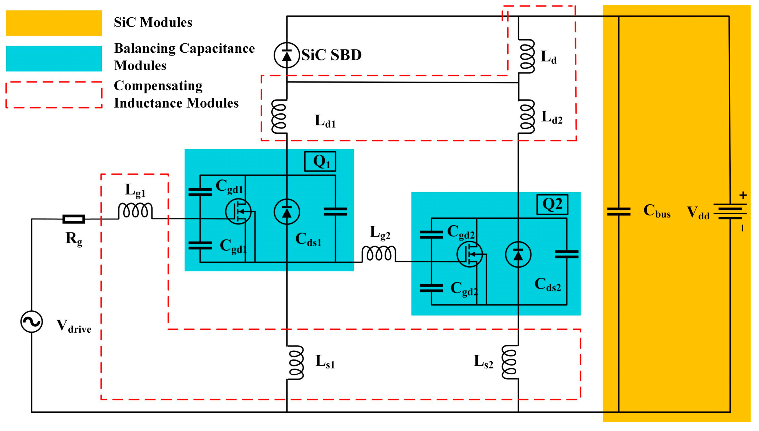
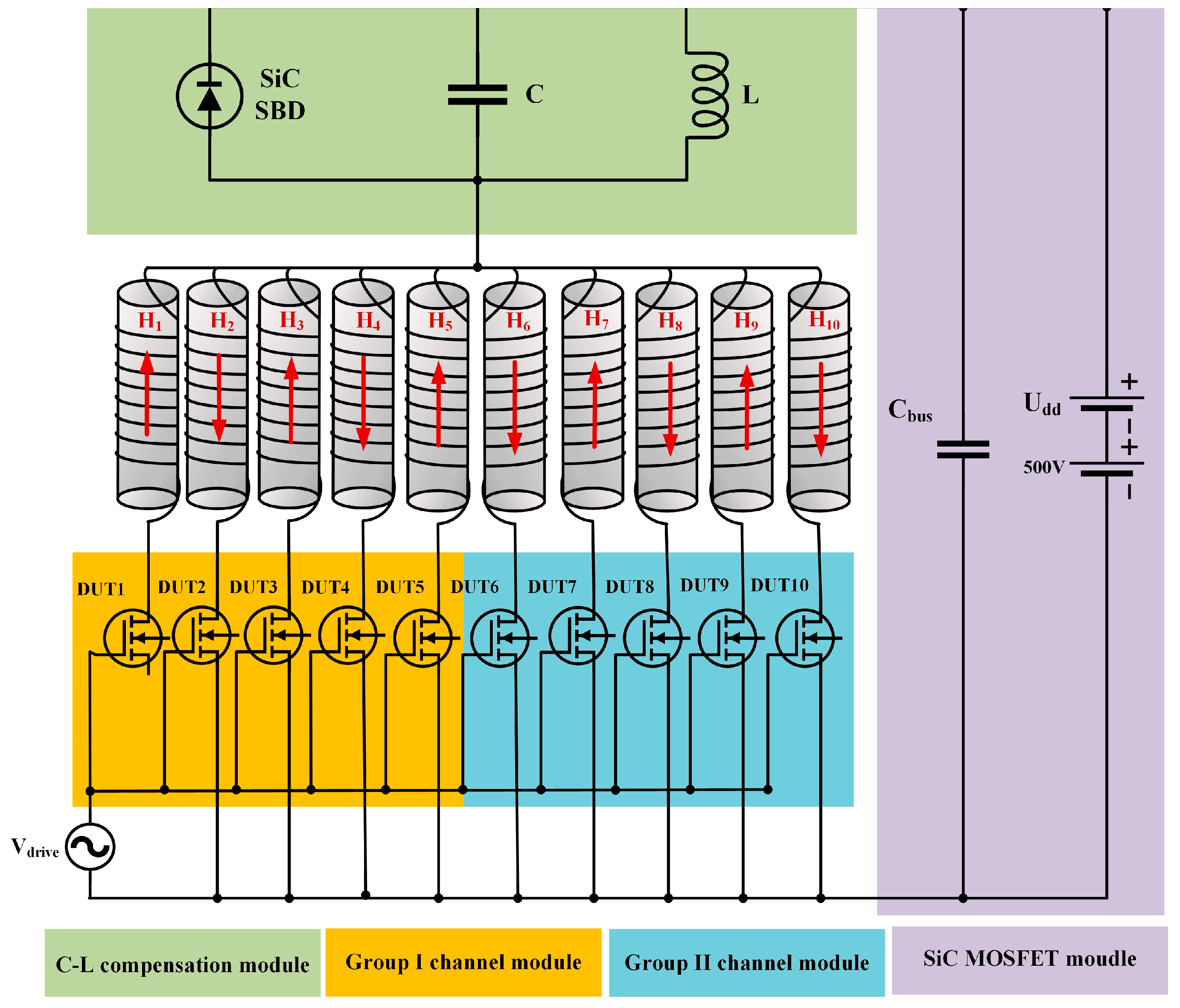
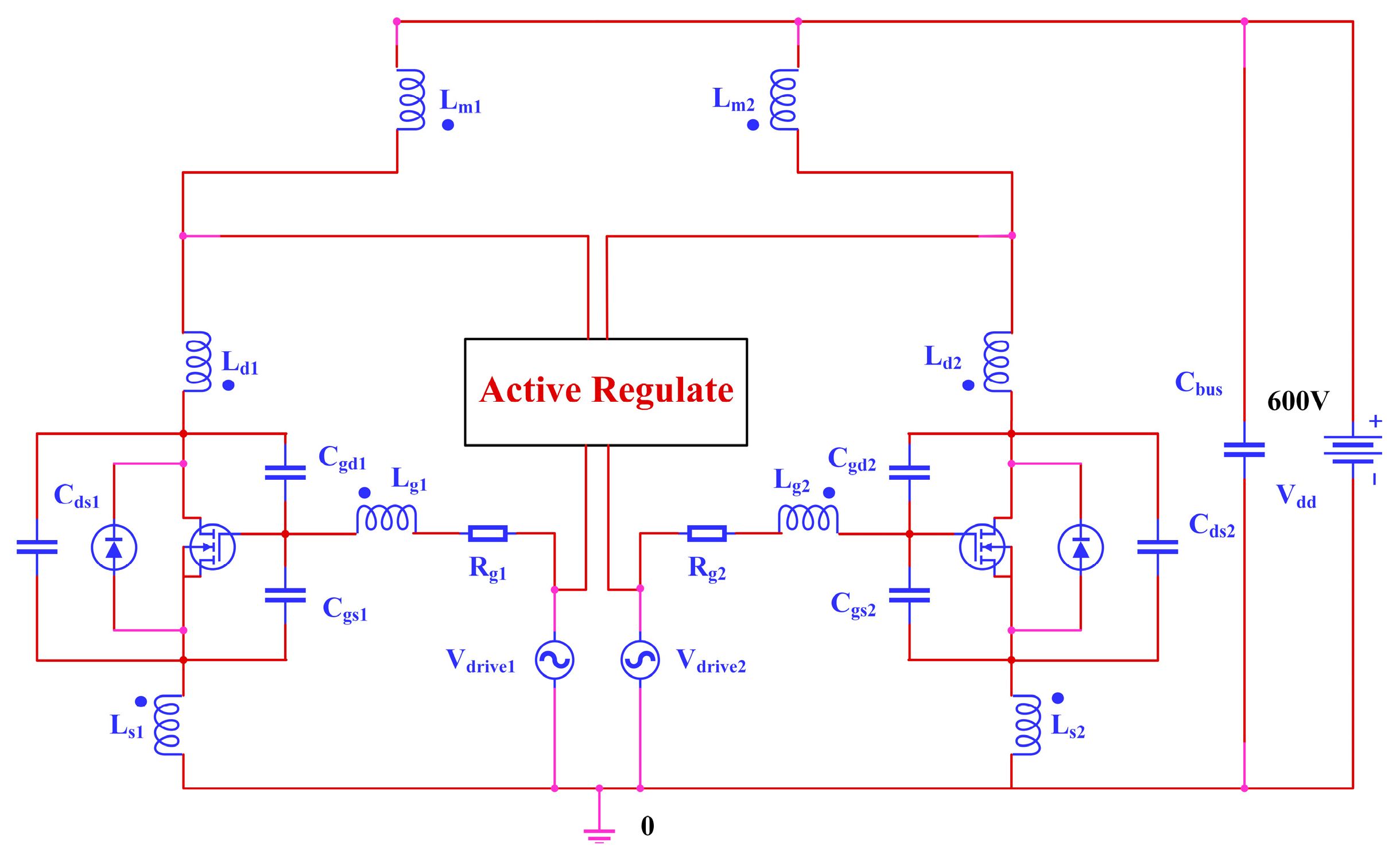
2.1. Design of the Improved Current-Sharing Imbalance Control Model

The improved current-sharing imbalance control model considering multiple parasitic parameters is designed, where the design of a parallel single-channel circuit is shown in Figure 1. According to the standard setting of multiple parasitic parameters of the double-pulse test circuit [20,21,22], the multiple parasitic parameters (Ciss, Coss, Crss, Ld, Lg, Ls, Cgs, Cgd, Cds, Rdson) are selected, respectively, as shown in Table 1. Cbus and Udd represent bus capacitance and DC load voltage, respectively, to maintain a constant output load voltage, where gm dynamically adjusts according to the variation in Cbus and Udd.
The test circuit for multiple parasitic parameters of high-frequency SiC modules considers input capacitance, output capacitance, and reverse transmission capacitance and is respectively designed to collect the input, output, and reverse transmission capacitance (Coss, Ciss, and Crss) [25,26,27], as shown in Figure 2a–c.

2.2. Principle of the Improved Current-Sharing imbalance Control Model

The principal design of parallel current sharing based on the single-channel magnetic ferrite inductance-combined gate drive circuit is obtained, as shown in Figure 3. The sum of the differential magnetic fluxes generated by electromagnetic induction is not zero in each branch on the parallel double-pulse test module, whilst the drain current id being unbalanced provides a certain inhibitory effect on rΔi [29,30]. The principal design of parallel current sharing based on the single-channel magnetic ferrite inductance-combined gate drive circuit is designed, as shown in Figure 3.
The optimized layout of PCB in the vertical multi-loop layout for DUT1–DUT10, the parallel power circuit layout, and the single-channel driving circuit layout is designed, as shown in Figure 4a–c. Parallel conductance modules with opposite currents are inserted between DUT1–DUT10 under the same current conditions to make the differential magnetic flux more obvious. The parameter settings of the optimized layout of PCB in the vertical multi-loop layout are shown in Table S2.
The greater current-sharing imbalance is attributed to the larger dispersion between parallel conductance modules, with more magnetic ferrite inductance modules used in parallel. The schematic diagram of the multi-channel parallel inductance model is shown in Figure 5. DUT1, DUT2⋯⋯DUT10 are, respectively, 1–10 parallel channels, and H1, H2⋯⋯H10 are the magnetic field intensities for DUT1–DUT10. The size and type of the magnetic ferrite inductance model are shown in Figure S2. As the magnetic ferrite inductance modules increase to n, the schematic diagram of the multi-channel parallel inductance model is obtained, as shown in Figure S3.
In parallel branches, the current in each 1-10 branch is id1, id2, id3, ⋯⋯ id10. The difference in parallel current sharing is Δiab (1 ≤ b < a ≤ 10), as shown in Equation (1):
Δ i a b = i d a i a b 1 a b 10
The magnetic field intensity excited by id1, id2, id3, ⋯⋯ id10 for each 1–10 branch is H1, H2······H10. The difference in parallel current sharing |Δiab| is, respectively:
Δ i 12 Δ i 23 Δ i 8 , 9 Δ i 9 , 10 0 = 1 10 l 1 + 2 l 2 l 1 0 0 0 0 0 2 l 2 l 1 + 2 l 2 l 1 0 0 0 0 2 l 2 2 l 2 2 l 2 2 l 2 l 1 + 2 l 2 l 1 0 2 l 2 2 l 2 2 l 2 2 l 2 2 l 2 l 1 + 2 l 2 l 1 1 1 1 1 1 1 1 H 1 H 2 H 8 H 9 H 10
Derived from Faraday’s law of electromagnetic induction, the induced voltages in the DUT1, DUT2 ⋯⋯ DUT10 parallel channels are represented by Uf1, Uf2, ⋯⋯ Uf10:
U f n = n d ϕ n d t 1 n 10
In matrix form:
U f 1 U f 2 U f 8 U f 9 U f 10 = S μ 0 μ r 10 2 l 1 + 2 l 2 l 1 0 0 0 0 0 2 l 2 l 1 + 2 l 2 l 1 0 0 0 0 2 l 2 2 l 2 2 l 2 2 l 2 l 1 + 2 l 2 l 1 0 2 l 2 2 l 2 2 l 2 2 l 2 2 l 2 l 1 + 2 l 2 l 1 1 1 1 1 1 1 1 d Δ i 12 d t d Δ i 23 d t d Δ i 8 , 9 d t d Δ i 9 , 10 d t 0
According to (1)–(4), the relative permeability of the magnetic ferrite inductance, μr, the area of the magnetic core, S, and the leakage inductance of magnetic ferrite inductance and winding, Lσ, act on id to suppress rΔi. In addition, the magnetic saturation and hysteresis of core inductance also induce the suppression of rΔi.

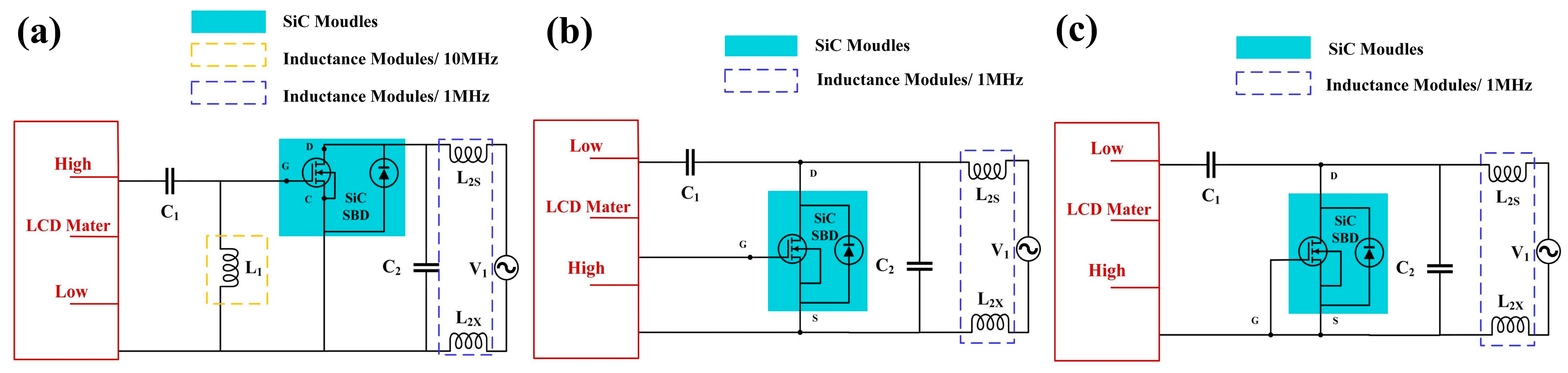
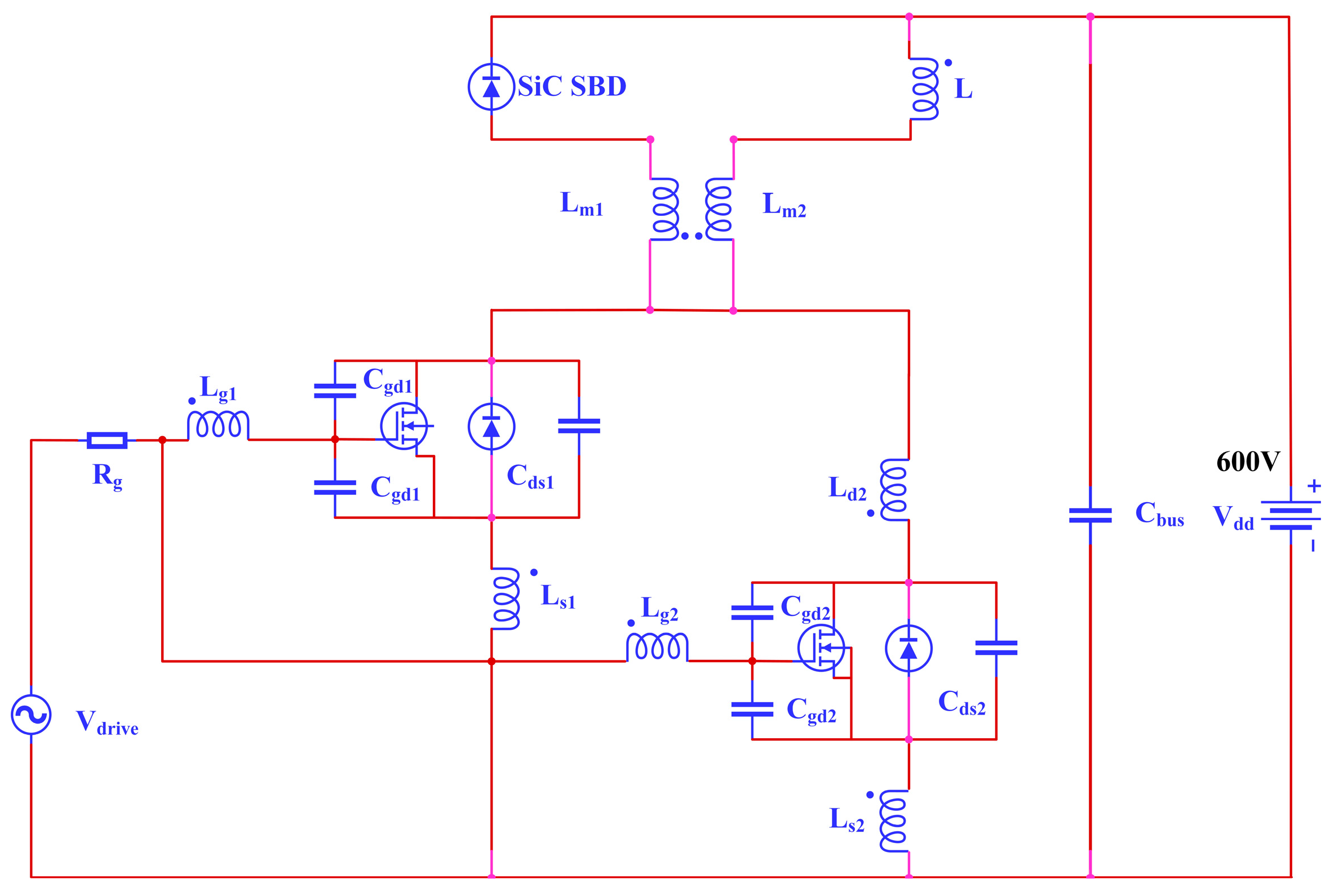
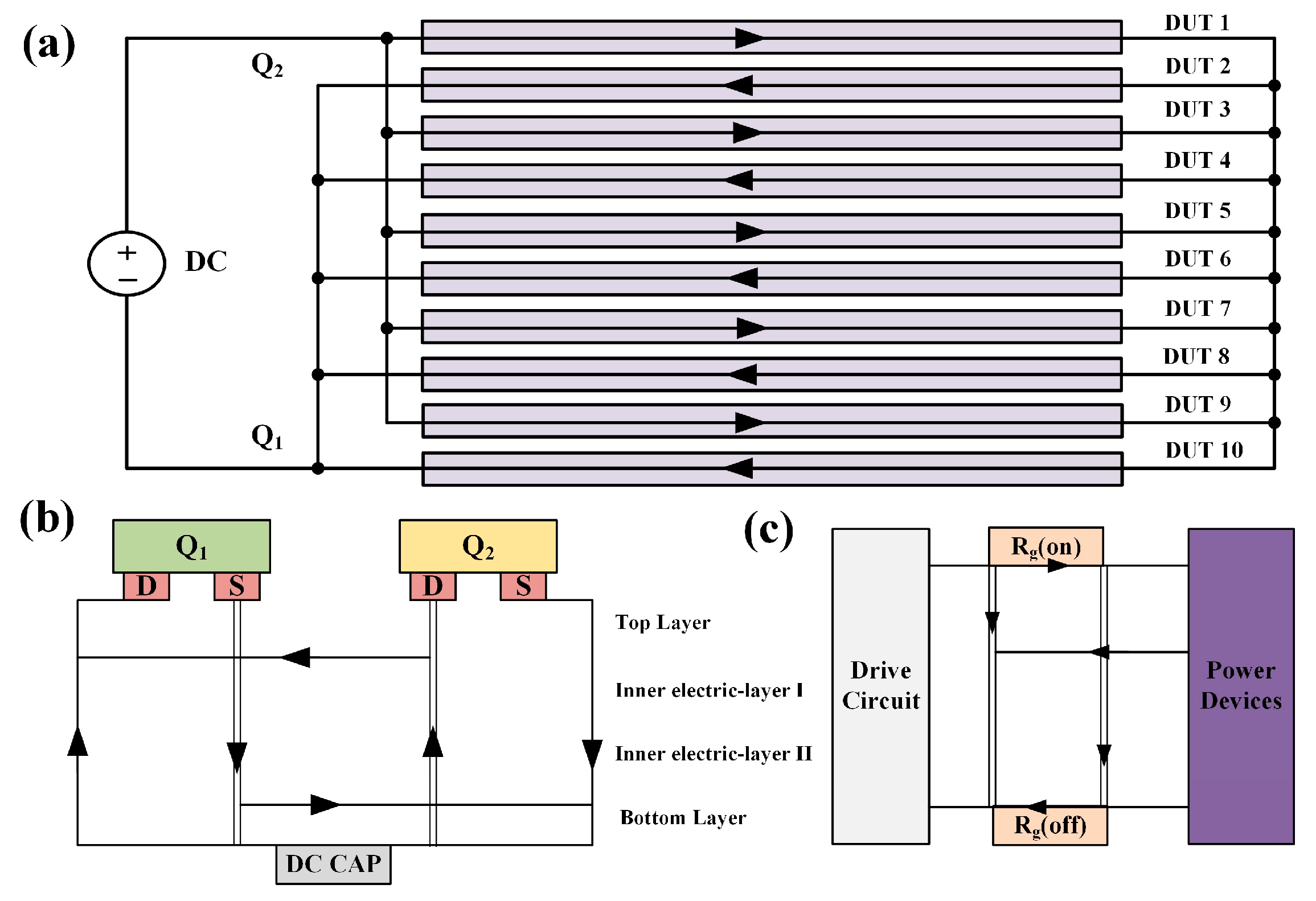
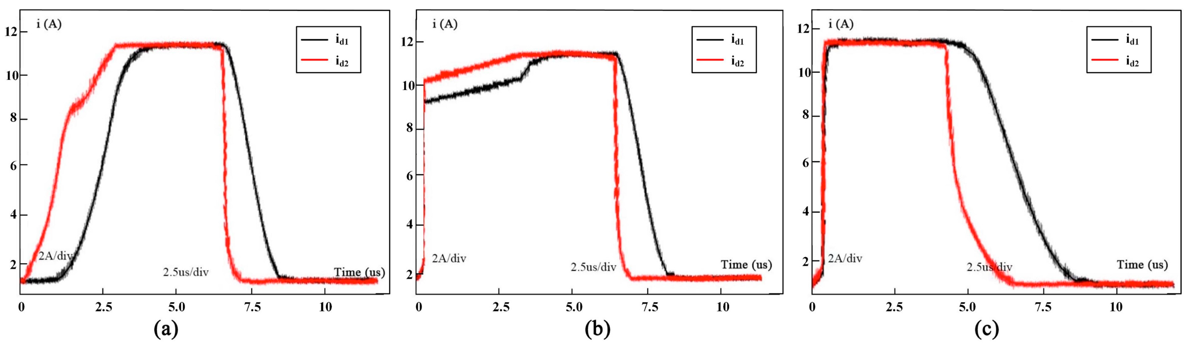
2.3. Improved Double-Pulse Detection Circuit Platform

The improved dual-pulse platform is built to study multiple parasitic parameters on the parallel current-sharing imbalance using the half-bridge module, as shown in Figure 6. The high (low)-level pulse, respectively, drives the turn-on (off) parallel branch circuit from pulse width modulation (PWM). Based on high (low)-level pulse signals, the driving gate driver outputs a dual-pulse waveform from the drive push–pull circuit and relies on the compensation capacitor to suppress the oscillation using the suppression circuit. The parallel bridge circuit maintains the electrical isolation during the turn-on (off) parallel state, and the output control circuit is connected to the C2M008120D SiC module for testing.

3. Results and Discussion

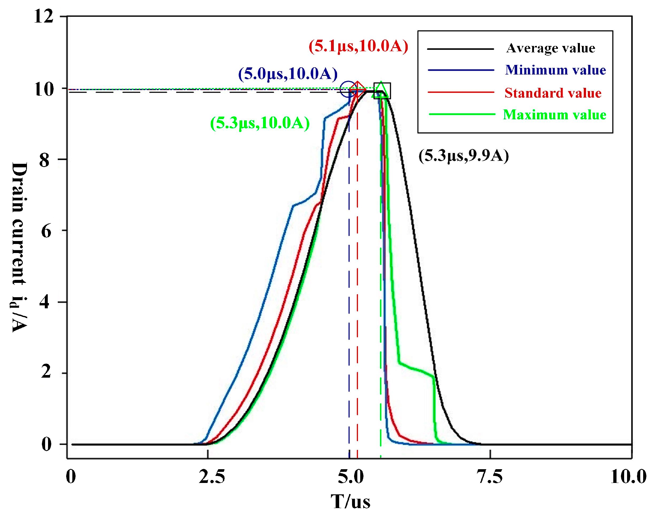
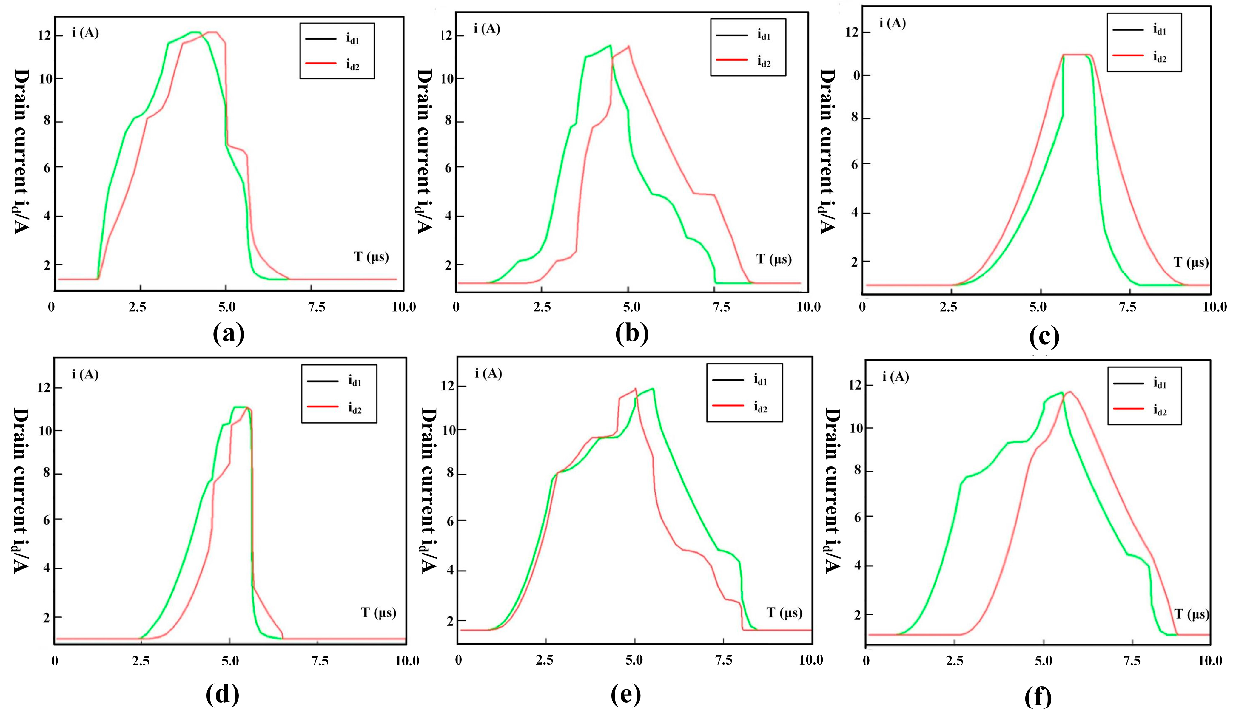
3.1. id/t Simulation on Different Lg

During the first set of parallel simulations, the standard value and other parameters of Lg1 on the first branch are set according to Table 1, and Lg2 in branch I is simulated with the maximum value, minimum value, and average value of the measurement results. The simulation curves of id and the maximum value, standard value, average value, and minimum value of Lg are obtained, as shown in Figure 7. At this time, the id on branch I and branch II are id1 and id2, respectively. id1 and id2 are expressed by:
i d = g f U g L g d i g d t V t h
where gf is the transconductance of the test module, and ig is the gate drive current.
The rΔi is:
r Δ i = i d 1 i d 2 = U g L g 1 d i g d t V t h U g L g 2 d i g d t V t h
A comparison of the simulation results shows that the branch with a small Lg has a faster Von and less id than the other branch. The maximum value, standard value, average value, and minimum value of Lg are set, respectively. The maximum values of id, 11.2 A, 11.2 A, 11.2 A, and 11.1 A, are obtained when Lg is at T = 5.5 μs, T = 5.0 μs, T = 3.7 μs, and T = 3.6 μs. According to Equation (6) for rΔi, it can be seen that Δid in the process of parallel switching is affected only when ΔLg is enormous, while Δid has no significant effect on ΔLg under static conditions.

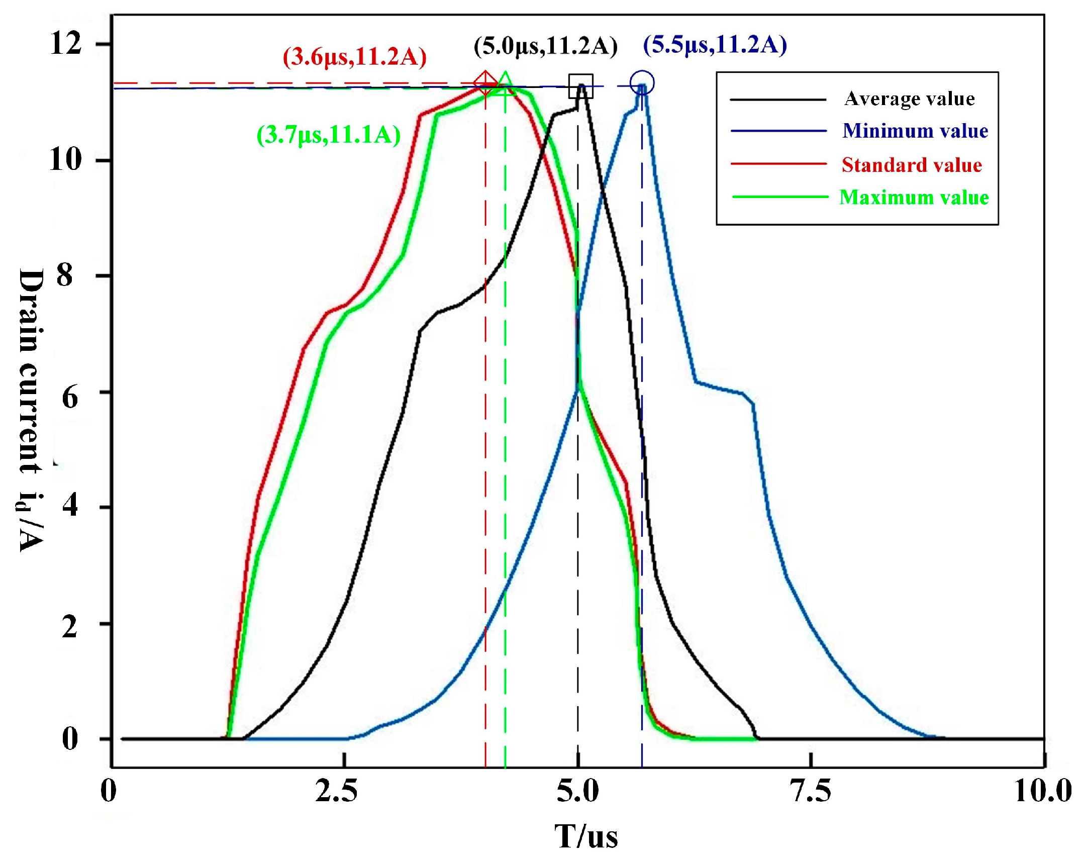
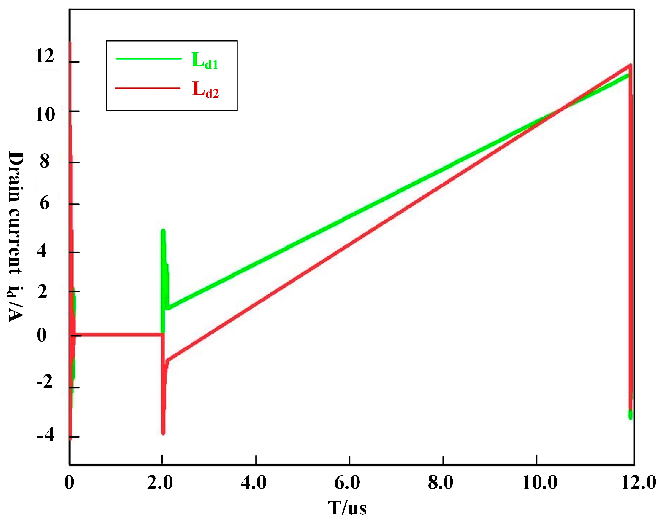
3.2. id/t Simulation on Different Ld

During the second set of parallel simulations, Ld affects the change rate of id. Ld and parasitic diode Cj form an oscillation circuit when turned on, and a spike in id appears. It forms a loop with Cds and charges simultaneously under turn-off conditions. An oscillation loop is formed while reducing the turn-off speed. Branch I is set as the standard value, while branch II is set as the maximum, minimum, and average values three times. The others are set according to Table 1 and remain constant. The simulation curves of id and the maximum value, standard value, average value, and minimum value of Ld are shown in Figure 8. The simulation curves of id with Ld1 and Ld2 (Ld on branch I and branch II) are shown in Figure 9 where Ld1 and Ld2 affect rΔi under dynamic and static conditions.
Equation (7) is obtained during turn on:
L d 1 d i d 1 d t + R d s o n 1 i d 1 = L d 2 d i d 2 d t + R d s o n 2 i d 2 = U d d L d i L d t
di/dt is the change rate of the drain current, and Rdson is the resistance after the test module is turned on.
When the total current is equal to the sum of id1/id2, Δid is derived:
Δ i d = i d 1 i d 2 = L d 1 L d 2 2 R d s o n U d d L
Ld1, Ld2 directly determines Δid at static state. A resonant circuit composed of Ld and the parasitic body diode generates current oscillation during the switching process.
The oscillation frequency, fzd, is expressed as:
f z d = 1 2 π L d C g d
Oscillation circuits I and II are obtained, composed of Ld (Ld1 and Ld2 on branch I and branch II in Figure 1) and Cgd (Cgd1 and Cgd2 on branch I and branch II in Figure 1), respectively.
A resonant circuit composed of Ld and Cds (Cds1 and Cds2 on branch I and branch II in Figure 1) is obtained during switching. Ld charges Cds at the resonant frequency of fxz. fxz is expressed as:
f z d = 1 2 π L d C d s
Ld affects rΔi after id rises (falls) during the switching process. The oscillation frequency and damping coefficient are reduced on the branch with a larger Ld.

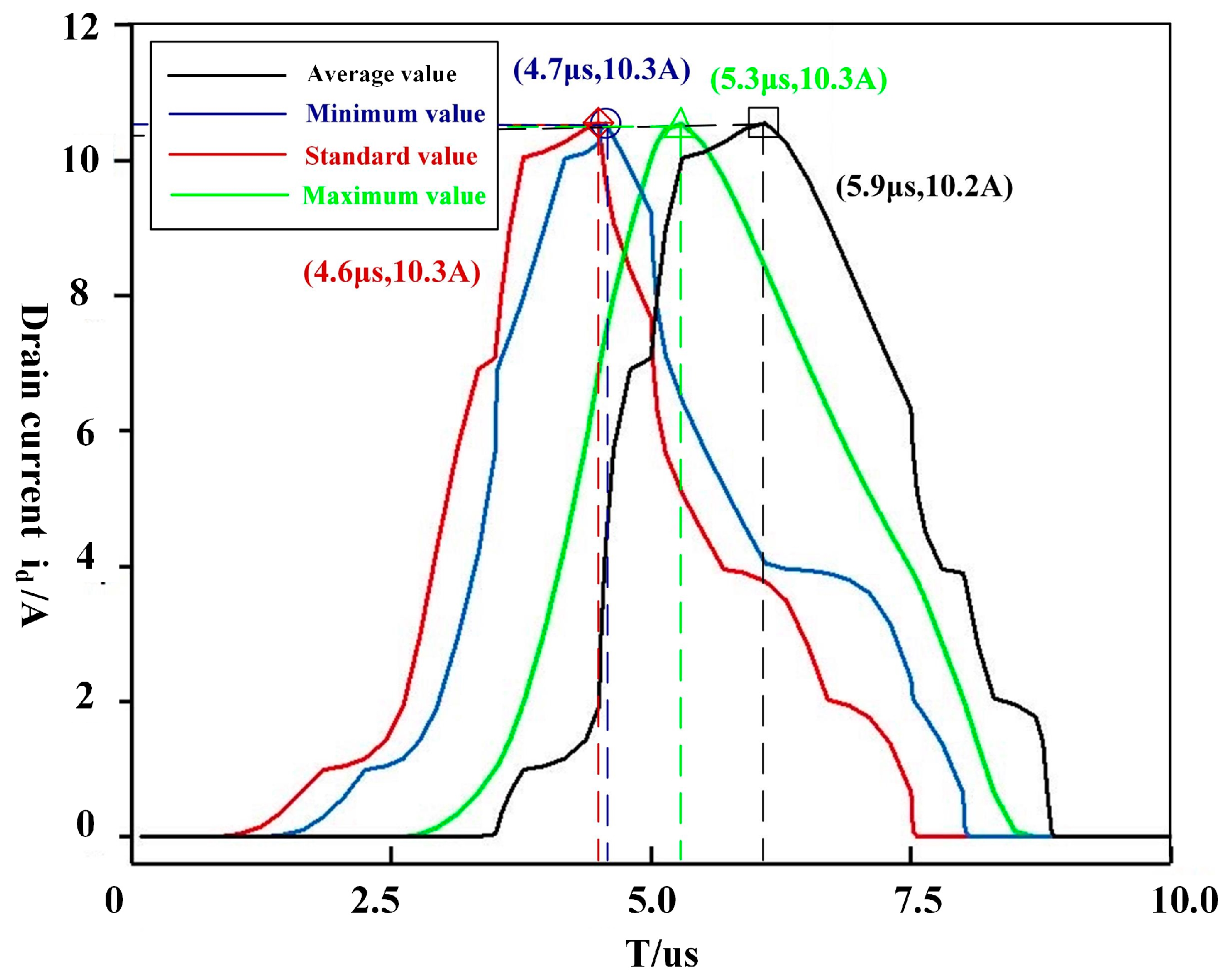
3.3. id/t Simulation on Different Ls

During the third set of parallel simulations, Ls on branch I is set as the standard value, and the values on branch II are set as the maximum, minimum, and average values of the measurement outcomes three times, respectively. The simulation curves of id and the maximum value, standard value, average value, and minimum value of Ls are obtained, as shown in Figure 10.
There is a nonlinear negative correlation between Ls and Ugs, and the change rate of id after conduction infinitely tends to zero, so the influence on rΔi under static conditions is reduced to zero. Ugs is expressed by:
U g s = U g i g R g L s d i d d t
At this time, rΔi is:
r Δ i = i d 1 i d 2 = U g i g R g L d i d 1 d t U g i g R g L d i d 2 d t
According to Equations (11) and (12), during the switching process of the branch with a larger Ls, the switching time is longer, id is smaller, and the current overshoot is also tiny.

3.4. id/t Simulation on Different Cgs

During the fourth set of parallel simulations, branch I and branch II are set to the standard values and the maximum, minimum, and average values, respectively. The simulation curves of id and the maximum value, standard value, average value, and minimum value of Cgs are shown in Figure 11.
id is very sensitive to Cgs during the switching process. On the branch with a smaller Cgs, the turn-on time is short, the fluctuation range of id is small, and the current overshoot is slight. After being turned on, Cgs has little effect on rΔi under static conditions. During the turn off of the SiC module, the branch with a smaller Cgs has a faster opening speed and a smaller id. The earlier the branch with a smaller Cgs is opened, the Vg first reaches the Vth. Since Cgs affects the change rate of Vg, Vg can reach Vth earlier on the branch with a smaller Cgs. The RC buffer circuit formed by Cgs and Rdson suppresses the occurrence of oscillation on id to reduce the charge/discharge and switching speed. On the branch with a larger Cgs, the charge/discharge and switching speed both decrease. The decrease in the switching speed increases the switching frequency of the test module. The occurrence of rΔi is increased by Cgs, affecting the change rate of Vg. The turn-on speed of the branch is slower when Cgs is larger.

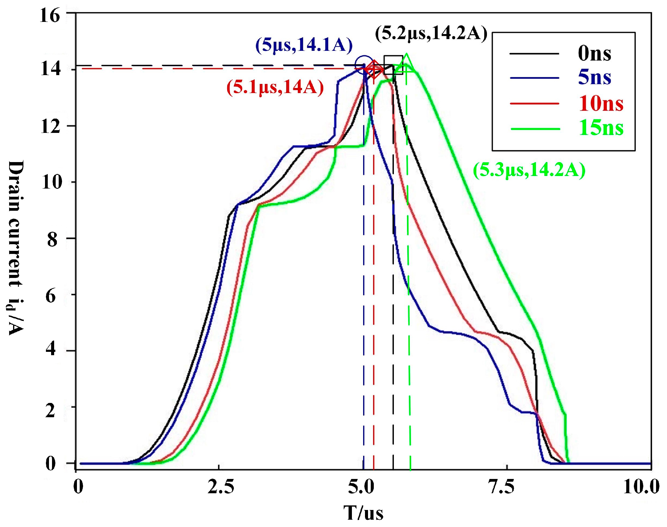
3.5. id/t Simulation on Different td

During the fifth set of parallel simulations, td is set to 0 on branch I, and td is set to 5 ns, 10 ns, and 15 ns, respectively, on branch II. The simulation curves of id and the 0 ns, 5 ns, 10 ns, and 15 ns values of td are acquired, as shown in Figure 12. id reaches the maximum values of about 14.1 A, 14.0 A, 14.2 A, and 14.2 A at 5 μs, 5.1 μs, 5.2 μs, and 5.3 μs, respectively, when td is 0 ns, 5 ns, 10 ns, and 15 ns, respectively. The rΔi increases as td increases. The turn-on speed of the double-pulse parallel test module is faster, and rΔi is smaller during the turn-on process of the branch with a smaller td. td shall be minimized to ensure parallel current-sharing imbalance control during double-pulse driving independently in parallel.

3.6. id/t Simulation on Different Von

Von is set to 18–20 V, which can effectively ensure the effective switching process of the double-pulse parallel test module. The branch with a larger Von has a faster switching speed and bears a greater id. gf is the ratio between id and Vg, being the slope of its curve. The larger gf means that Vg has stronger control over id. Vg is larger, leading to a stronger control ability and a faster switching speed. Von can effectively adjust id in the static state by Rdson. The branch that bears the whole id will damage the double-pulse parallel test module as the Von signals differ greatly.
In the turn-on state, id is:
i d = g f U g s V t h
At this point, rΔi is:
r Δ i = i d 1 i d 2 = g f U g L g 1 i g V t h g f U g L g 2 i g V t h

3.7. id/t Simulation on Different Rg

During the sixth set of parallel simulations, Rg is set to 10 Ω on branch I, and Rg is set to 5 Ω, 15 Ω, and 20 Ω, respectively, on branch II. The others are set according to Table 1. The simulation results are shown in Figure 13.

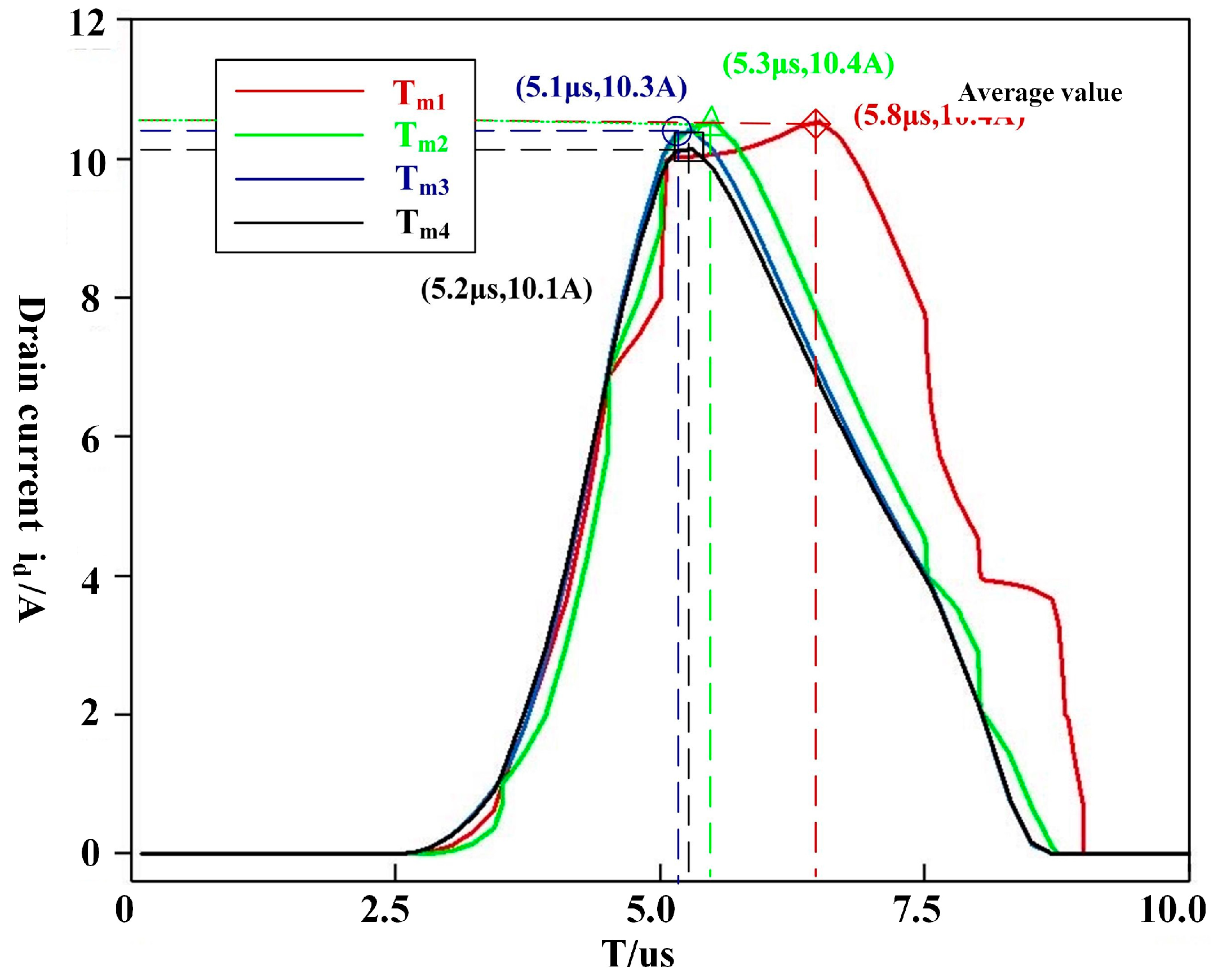
3.8. id/t Simulation on Different ΔTm

Rdson and ΔTm are larger, while id is smaller when the others are the same on the branch with a higher Tm. Vth of the test module shows a downward trend as Tm increases. Vth decreases and ion increases on the branch with a higher Tm. Setting Tm1 > Tm2 > Tm3 > Tm4, the relationship between id and Tm is shown in Figure 14. When Tm1, Tm2, Tm3, and Tm4 are set as 5.8 μs, 5.3 μs, 5.1 μs, and 5.2 μs, respectively, the maximum values of id are 10.4 A, 10.4 A, 10.3 A, and 10.1 A.

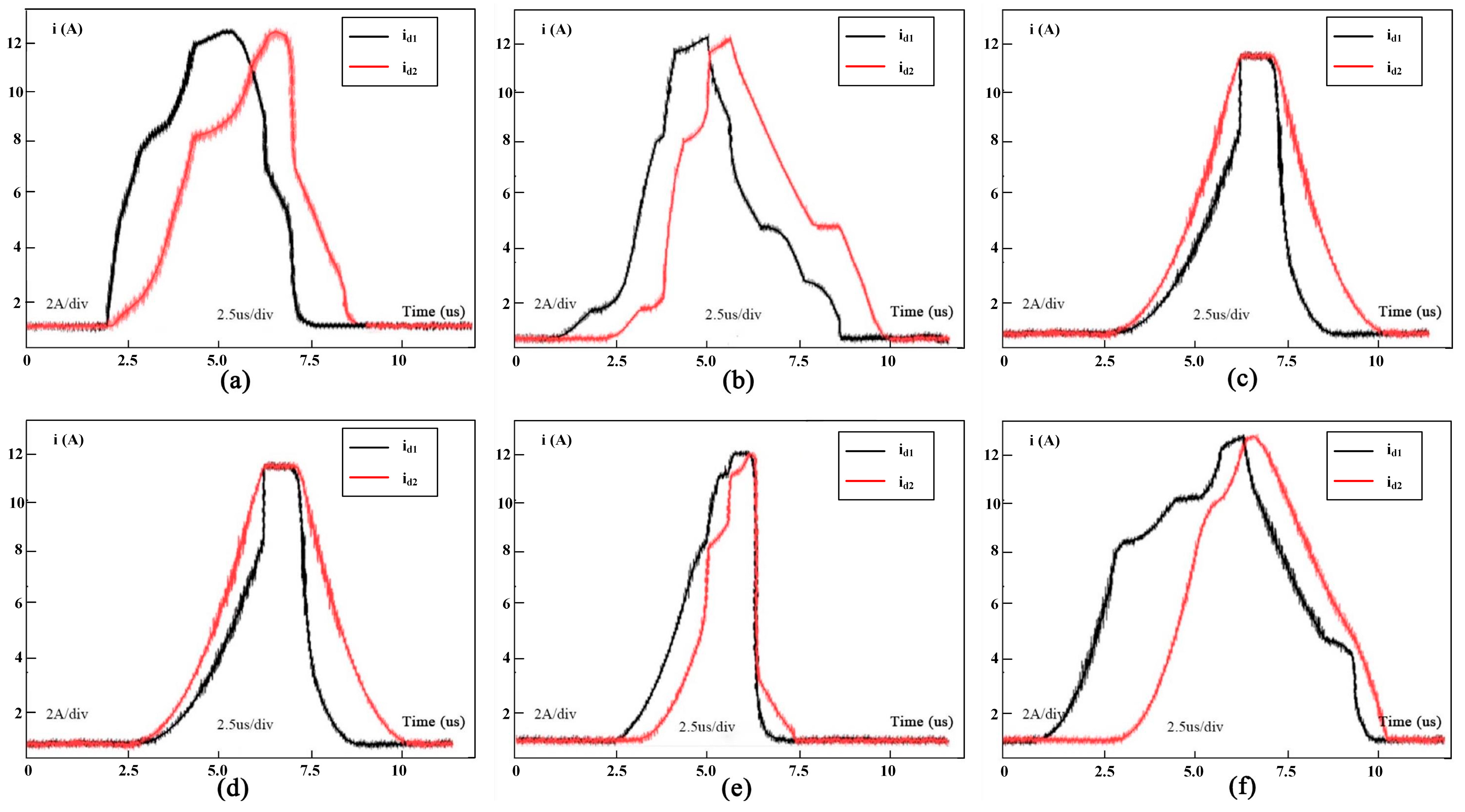
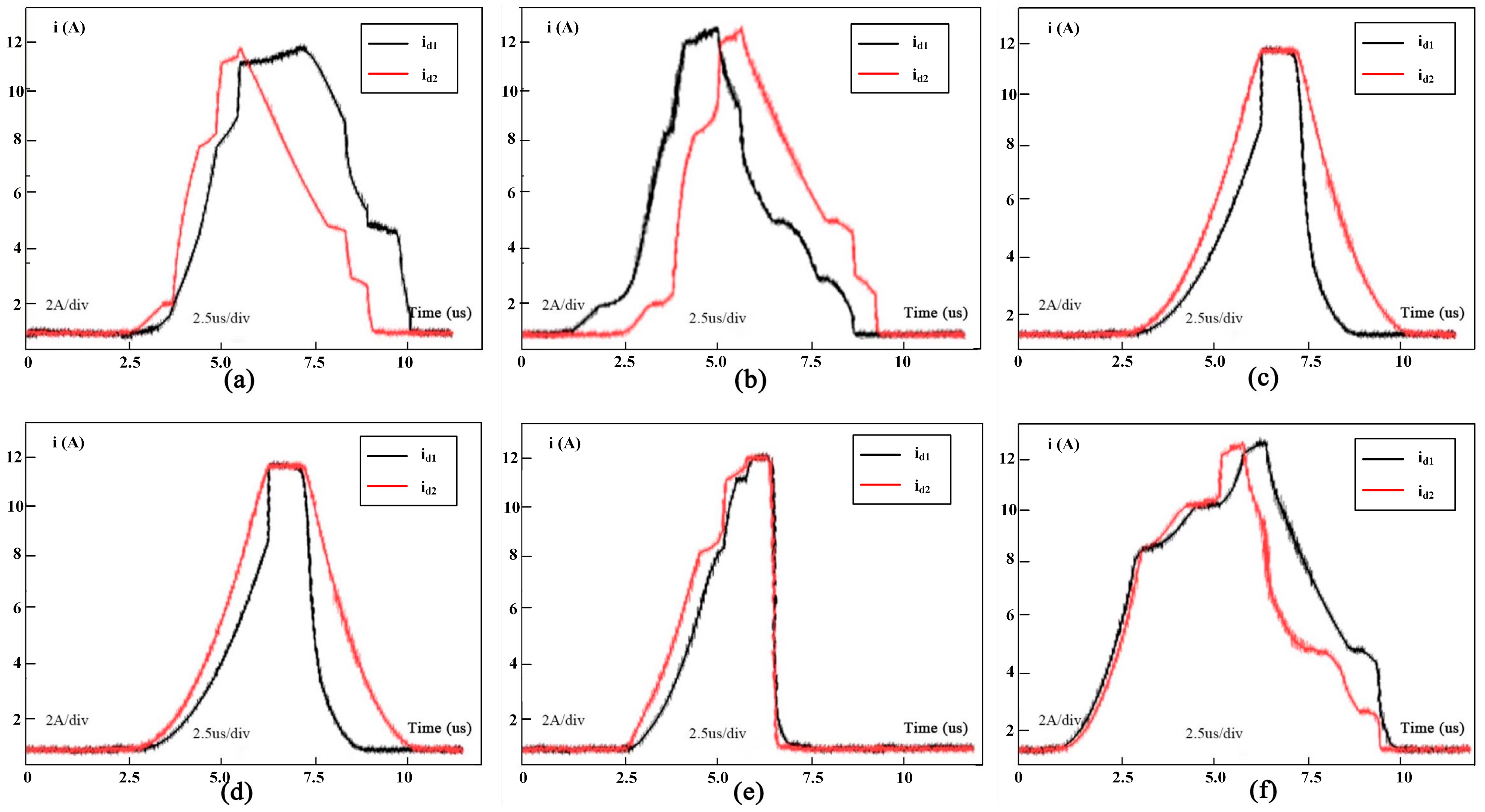
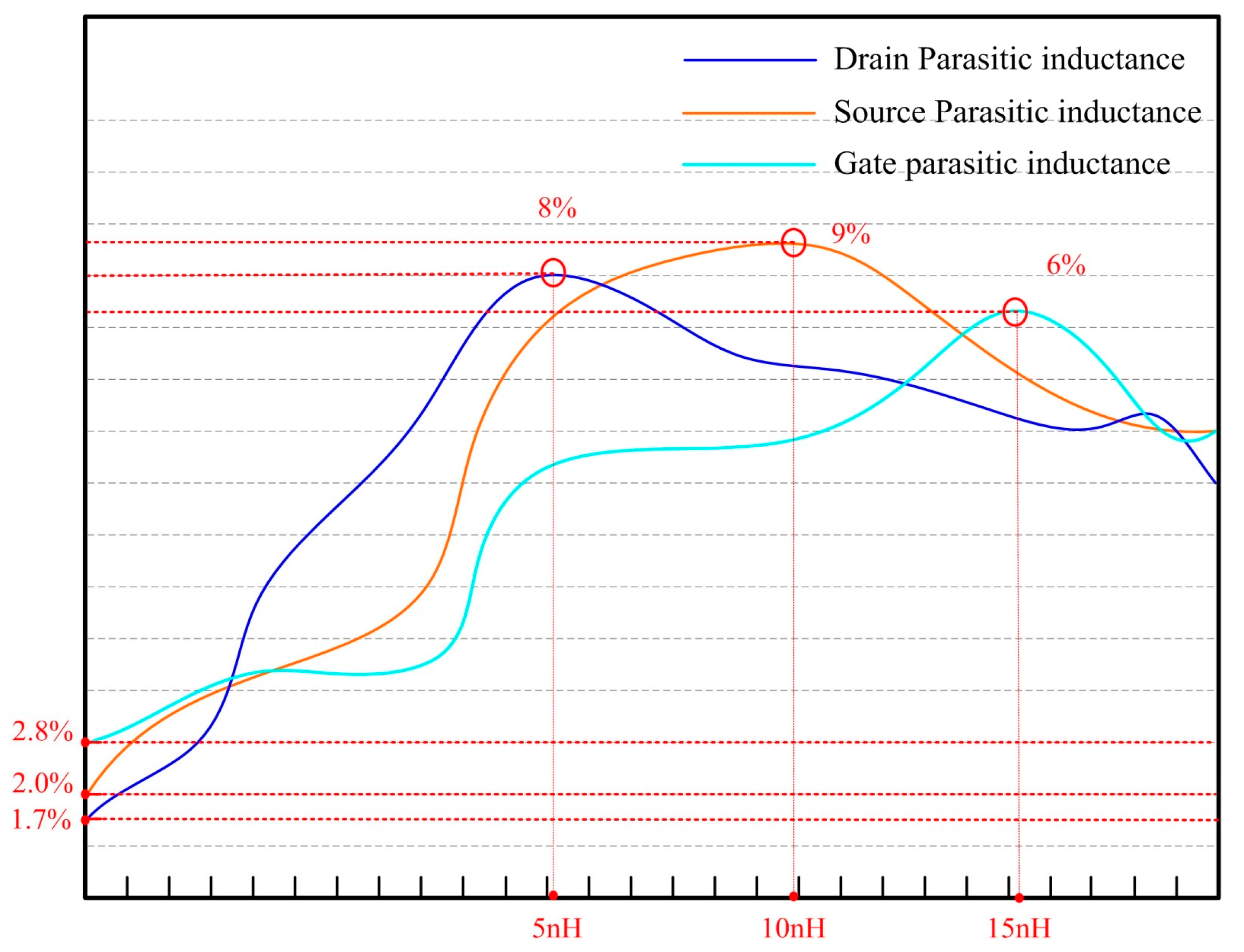
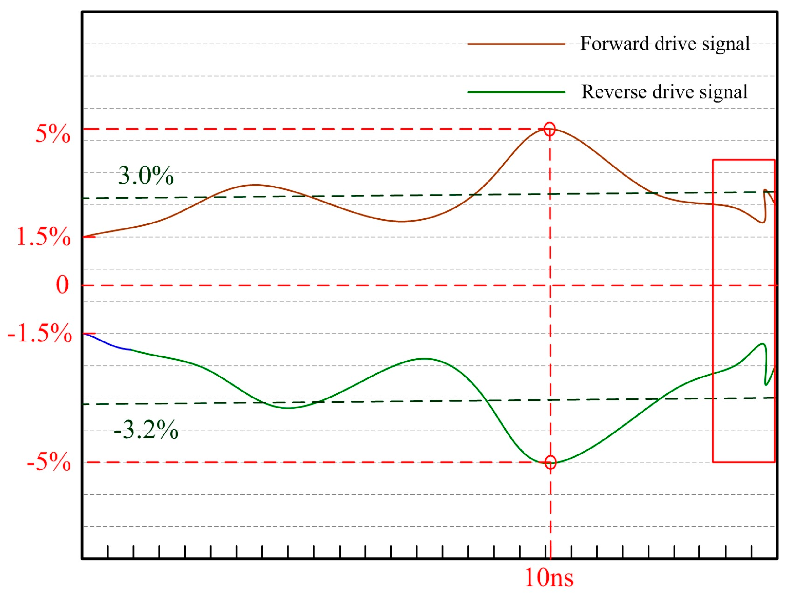
4. Joint Simulation of Multiple Parasitic Parameters in the Double-Pulse Test Circuit

The simulation object is the extreme value of the multiple parasitic parameters on rΔi during the joint simulation process. The joint simulation circuit of multiple parasitic parameters is designed, as shown in Figure 15.
The active control system of the gate drive circuit is connected to the drain first during the joint-simulation process. It takes a specific reaction time from detecting the parallel current-sharing imbalance to the beginning of suppression. The reaction time is about 0 due to the magnetic ferrite inductance connected to the wound coil of the drain. The rΔi of the magnetic ferrite inductance is relatively weak, and rΔi is not affected by hysteresis and other factors normally. The gate circuit actively regulates rΔi and acts on the gate drive circuit to reduce rΔi. The simulation results show that the parallel current-sharing control model based on magnetic ferrite inductance and the parallel current-sharing control model based on a gate drive circuit both can effectively reduce rΔi. The rΔi is reduced by 2–4.2%, as shown in Figure 16a–f. The combination of the two models can alleviate the hysteresis caused by a high switching frequency and reduce the requirements for the computing power of FPGA.
The parasitic parameters of the test channels numbered DUT1 and DUT10 are consistent, so DUT1 and DUT10 are selected for this experiment and verification. The measurement results are compared with the data manually, and the values of the parasitic parameters in the form of the external parasitic inductance and the connecting capacitance are changed to make the parameters involved in the test fluctuate within 10% of the range specified in the data manually, which is used to verify the simulation results, as shown in Figure 17 and Figure 18. During the experiment, the branch with more extensive parasitic parameters is labeled as 1, and the branch with smaller parasitic parameters is labeled as 2.
Using the consistency of the other parameters, except for the reference factors in the single- and joint-simulation experiments, each branch of the parallel double-pulse test module is driven solely to ensure that the driving signal can be regulated in two experiments, respectively. The optimal test channels in DUT1–DUT10 are selected for parasitic parameters (Ld, Lg, Ls, Cgs, td, Von, Ron, and ΔTm), as DUT9 and DUT10 are used as standard channels. Under the single- and joint-simulation experiments, the larger test data are marked as 1, while the smaller test data are marked as 2 to obtain the suppression effect on rΔi.
The maximum Lg is on DUT5, and the minimum Lg is on DUT7. The maximum Ld is on DUT3, and the minimum Lg is on DUT5. The maximum Ls is on DUT4, and the minimum Ls is on DUT3. The maximum Cgs is on DUT1, and the minimum Lg is on DUT8. The parasitic parameters (Ld, Lg, Ls, Cgs, td, Von, Ron, and ΔTm) are tested independently on the DUT1–DUT10 channels by the parallel double-pulse test modules, respectively. The single- and joint-simulation suppression experiments of single magnetic ferrite inductance and the single- and joint-simulation suppression experiments of magnetic ferrite inductance combined with a gate drive circuit are carried out, as shown in Figure 19 and Figure 20.
The standard values of parasitic parameters are set according to Table 1. Ls, Ld, Lg, Cgs, Tdely, Ron, Von, and Tm are respectively set as 10 nH, 6 nH, 15 nH, 25 pF, 10 ns, 10 Ω, 18 V, and 35 °C to realize that the standard value of the parallel current is maintained at 10 A. The rΔi on multiple parasitic parameters is shown in Table S3. It is obvious that Ls, Ld, and Lg optimize the parallel current-sharing imbalance; the rΔi is generally between 5% and 10%. Lg has a minimal influence on rΔi; the rΔi is about 6%, while Ld has a maximal influence on the parallel current-sharing imbalance; the rΔi is about 9%. Cgs is the most sensitive to the parallel current-sharing imbalance. The rΔi is about 11% by increasing Cgs every 5 pF, as shown in Table S4. The parallel current-sharing imbalance is reversed by changing the delay direction of the driving signals on branch I and branch II. The rΔi is 0 as the delay of the driving signal is 0. Ron and Von regulate rΔi through the gate drive circuit; the rΔi is about 5% and 6%, respectively. Tm optimizes the parallel current-sharing imbalance through the changes in device performance; the rΔi is about 7%.
As shown in Figure 21, the rΔi of Ld, Lg, and Ls on the parallel current-sharing imbalance is nonlinear. The initial rΔi of Ls, Ld, and Lg is 1.7%, 2.0%, and 2.8%, respectively. Ld, Lg, and Ls are independently set to 5 nH, 10 nH, and 15 nH; the rΔi reaches the maximum value, which is 8%, 9%, and 6% respectively.
The delay of the forward/reverse driving signal impacts rΔi symmetrically, as shown in Figure 22. The interference of other irrelevant signals leading to the existence of fluctuation deviation is shown in the red box of Figure 22. The rΔi reaches the maximum/minimum values of 5% and −5.3% when the forward and reverse driving signals are delayed by 10 ns. The average values of rΔi on the forward and reverse driving signals are approximately 3.0% and −3.2% because of the existence of irrelevant signal interference. The average value of rΔi is approximately equal to the average value of rΔi on the reverse driving signal on the forward driving signal, assuming that the interference of irrelevant signals is excluded. The forward/reverse driving signals affect the parallel current-sharing imbalance similarly, while the direction is opposite.

5. Conclusions

The parallel current-sharing imbalance affected by multiple parasitic parameters (Ld, Lg, Ls, Cgs, td, Von, Ron, and ΔTm) wa investigated by single and joint simulations and suppression experiments. It was found that the rΔi of Ld, Lg, and Ls is between 5% and 10%. When Ld, Lg, and Ls were independently set to 5 nH, 10 nH, and 15 nH, rΔi reached the maximum value, which is 8%, 9%, and 6% respectively. The effect of the parasitic inductance of the parallel double-pulse test module on rΔi was Lg > Ls > Ld. The rΔi of the Cgs was approximately 9% to 11%. The rΔi reached a maximum of about ±5% as the forward/reverse driving signals were delayed by 10 ns. The rΔi is smaller with a larger Von, smaller Ron, and larger ΔTm. This work complements the investigation of current-sharing imbalance with multiple parasitic parameters using the sum of the differential magnetic flux. An improved parallel current-sharing imbalance control model consisting of ferrite inductance and a gate drive circuit was proposed, which respectively reduced rΔi by more than 5% and 2–4.2%, compared with using a gate drive circuit alone and using magnetic ferrite inductance solely. The model is expected to be used to suppress the occurrence of high-frequency parallel current-sharing imbalances, especially.

Supplementary Materials

The following supporting information can be downloaded at: https://www.mdpi.com/article/10.3390/machines11020197/s1, Figure S1: Multi-channel parasitic inductances and capacitances of C2M008120D chip: (a) Test results of Ciss, Coss, and Crss; (b) Test results of Ls, Lg, and Ld; Figure S2: The size and type of the magnetic ferrite inductance model; Figure S3: Schematic diagram of multi-module parallel test using magnetic ferrite inductance; Figure S4: Single-loop PSpice model in high-frequency applications; Figure S5: Current signal integration circuit; Figure S6: Parallel current equalization with multiple parasitic parameters based on ferrite inductor: (a) gate parasitic inductance Lg; (b) drain parasitic inductance Ld; (c) source parasitic inductance Ls; (d) gate-source parasitic inductance Cgs; (e) drain-source parasitic inductance Cds; (f) gate-drain parasitic inductance Cgd; Figure S7: Suppression of parallel current-sharing imbalance caused by mismatch of driving resistors: (a) single ferrite inductance on parasitic parameters; (b) ferrite inductance combined grid drive circuit on parasitic parameters; Table S1: Comparison of other research institutions/researchers on parallel double-pulse circuit models; Table S2: The single-loop parameters of DUT1-DUTn in optimized vertical multi-loop layout; Table S3: Comparison of rΔi on multiple parasitic parameters.; Table S4: The variation of rΔi on Cgs.

Author Contributions

Conceptualization, Y.L. (Yuqiang Li) and H.L.; methodology, H.T.; software, N.X.; validation, Y.L. (Yuqiang Li) and Y.L. (Yuhong Li); formal analysis, Y.L. (Yuhong Li) and H.T.; investigation, Y.L. (Yuhong Li) and H.T.; writing—original draft preparation, Y.L. (Yuhong Li); writing—review and editing, Y.L. (Yuqiang Li) and H.T.; supervision, Q.Z.; project administration, Y.L. (Yuqiang Li); funding acquisition, Y.L. (Yuqiang Li), J.W. and H.L. All authors have read and agreed to the published version of the manuscript.

Funding

This research was funded by the project of the the National Natural Science Foundation of China, grant number (11804249, 61804107) and the Natural Science Foundation of Tianjin City, grant number (18JCQNJC03700, 18JCYBJC85400, 20JCQNJC00180).

Institutional Review Board Statement

Not applicable.

Informed Consent Statement

Not applicable.

Data Availability Statement

Not applicable.

Conflicts of Interest

The authors declare no conflict of interest.

References

  1. Matsui, K.; Murai, Y.; Watanabe, M.; Kaneko, M.; Ueda, F. A pulsewidth-modulated inverter with parallel connected transistors using current-sharing reactors. IEEE Tran. Power Electron. 1993, 8, 186–191. [Google Scholar] [CrossRef]
  2. Cooper, J.A.; Melloch, M.R.; Singh, R.; Agarwal, A.; Palmour, J.W. Status and prospects for SiC power MOSFETs. IEEE Trans. Electron. Devices 2002, 49, 658–664. [Google Scholar] [CrossRef]
  3. Li, H.; Munk-Nielsen, S.; Bȩczkowski, S.; Wang, X. A novel DBC layout for current imbalance mitigation in SiC MOSFET multichip power modules. IEEE Tran. Power Electron. 2016, 31, 8042–8045. [Google Scholar] [CrossRef]
  4. Miao, W.; Fang, L.; Xu, L. A double-end sourced wire-bonded multichip SiC MOSFET power module with improved dynamic current sharing. IEEE Trans. Emerg. Sel. Topics Power Electron. 2017, 5, 1828–1836. [Google Scholar]
  5. Lelis, A.; Habersat, D.; Urciuoli, D.; Schroen, E.; Nouketcha, F.; Green, R. Updated key issues for SiC MOSFET reliability. Meet. Abstr. 2020, MA2020-02, 1838. [Google Scholar] [CrossRef]
  6. Abuogo, J.; Zao, Z.; Ke, J. Linear regression model for screening SiC MOSFETs for paralleling to minimize transient current imbalance. IOP Conf. Ser. Mater. Sci. Eng. 2019, 533, 012011. [Google Scholar] [CrossRef]
  7. Sadik, D.P.; Colmenares, J.; Tolstoy, G.; Peftitsis, D.; Bakowski, M.; Rabkowski, J.; Nee, H.P. Short-Circuit Protection Circuits for Silicon-Carbide Power Transistors. IEEE Trans. Ind. Electron. 2016, 63, 1995–2004. [Google Scholar] [CrossRef]
  8. Liu, X.G.; He, J.; Gu, L.; Hao, H.K.; Zhao, A.Q.; Tan, Q.Y. Research on current imbalance law of bus-bar caused by inter-turn short circuit of dry-type air-core reactor. IOP Conf. Ser.: Earth Envmagnetic. Sci. 2018, 188, 012036. [Google Scholar] [CrossRef]
  9. Ji, S.; Laitinen, M.; Huang, X.; Sun, J.; Giewont, W.; Wang, F.; Tolert, L.M. Short-Circuit Characterization and Protection of 10-kV SiC MOSFET. IEEE Tran. Power Electron. 2019, 34, 1755–1767. [Google Scholar] [CrossRef]
  10. Zhang, H.; Guo, H.-X.; Zhang, F.-Q.; Pan, X.-Y.; Liu, Y.-T.; Gu, Z.-Q.; Ju, A.-A.; Ouyang, X.-P. Sensitivity of heavy-ion-induced single event burnout in SiC MOSFET. Chin. Phys. B 2020, 31, 018501. [Google Scholar] [CrossRef]
  11. Tega, N.; Sato, S.; Shima, A. Comparison of extremely high-temperature characteristics of planar and three-dimensional SiC MOSFETs. IEEE Electron Device Lett. 2019, 40, 1382–1384. [Google Scholar] [CrossRef]
  12. Zeng, Z.; Shao, W.; Hu, B.; Kang, S.; Liao, X.; Li, H.; Ran, L. Active current sharing of paralleled SiC MOSFETs by coupling inductors. Proc. CSEE 2017, 37, 2068–2080. [Google Scholar]
  13. Xun, Q.; Xun, B.; Li, Z.; Wang, P.; Cai, Z. Application of SiC power electronic devices in secondary power source for aircraft. Renew. Sust. Energ. Rev. 2017, 70, 1336–1342. [Google Scholar] [CrossRef]
  14. Hu, J.; Alatise, O.; Gonzalez, J.A.O.; Bonyadi, R.; Alexakis, P.; Ran, L.; Mawby, P. Robustness and Balancing of Parallel-Connected Power Devices: SiC Versus CoolMOS. IEEE Trans. Ind. Electron. 2016, 63, 2092–2102. [Google Scholar] [CrossRef]
  15. Lim, J.-K.; Peftitsis, D.; Rabkowski, J.; Bakowski, M.; Nee, H.-P. Analysis and experimental verification of the influence of fabrication process tolerances and circuit parasitics on transient current sharing of parallel-connected SiC JFETs. IEEE Tran. Power Electron. 2014, 29, 2180–2191. [Google Scholar] [CrossRef]
  16. Lu, Z.; Li, C.; Zhu, A.; Luo, H.; Li, C.; Li, C.; He, X. Medium voltage soft-switching DC/DC converter with series-connected SiC MOSFETs. IEEE Tran. Power Electron. 2021, 36, 1451–1462. [Google Scholar] [CrossRef]
  17. Bahmani, M.A.; Thiringer, T.; Rabiei, A.; Abdulahovic, T. Comparative study of a multi-MW high-power density DC transformer with an optimized high-frequency magnetics in all-DC offshore wind farm. IEEE Trans. Power Deliv. 2016, 31, 857–866. [Google Scholar] [CrossRef]
  18. Scheuermann, U. Reliability challenges of automotive power electronics. Microelectron. Reliab. 2009, 49, 1319–1325. [Google Scholar] [CrossRef]
  19. Ke, J.; Zhao, Z.; Sun, P.; Zou, Q.; Cui, X.; Yang, F. Influence of devices parameters on the current sharing of paralleled SiC MOSFETs using statistics analysis. Semicond. Tech. 2018, 43, 181–187. [Google Scholar]
  20. Li, Y.; Liang, M.; Chen, J.G.; Zheng, T.Q.; Guo, H.B. A low gate turn-off impedance driver for suppressing crosstalk of SiC MOSFET based on different discrete packages. IEEE Trans. Emerg. Sel. Topics Power Electron. 2019, 7, 353–365. [Google Scholar] [CrossRef]
  21. Bahman, A.S.; Iannuzzo, F.; Uhrenfeldt, C.; Blaabjerg, F.; Munk-Nielsen, S. Modeling of short-circuit-related thermal stress in aged IGBT modules. IEEE Trans. Ind. Appl. 2017, 53, 4788–4795. [Google Scholar] [CrossRef]
  22. Li, H.; Zhou, W.; Wang, X.; Munk-Nielsen, S.; Li, D.; Wang, Y.; Dai, X. Influence of paralleling dies and paralleling half-bridges on transient current distribution in multichip power modules. IEEE Tran. Power Electron. 2018, 33, 6483–6487. [Google Scholar] [CrossRef]
  23. Ji, S.; Zheng, S.; Wang, F.; Tolbert, L.M. Temperature-dependent characterization, modeling, and switching speed-limitation analysis of third-generation 10-kV SiC MOSFET. IEEE Tran. Power Electron. 2018, 33, 4317–4327. [Google Scholar] [CrossRef]
  24. Mao, Y.; Miao, Z.; Wang, C.; Ngo, K.D.T. Balancing of peak currents between paralleled SiC MOSFETs by drive-source resistors and coupled power-source inductors. IEEE Trans. Ind. Electron. 2017, 64, 8334–8343. [Google Scholar] [CrossRef]
  25. Mao, Y.; Miao, Z.; Wang, C.; Ngo, K.D.T. Passive Balancing of peak currents between paralleled MOSFETs with unequal threshold voltages. IEEE Tran. Power Electron. 2017, 32, 3273–3277. [Google Scholar] [CrossRef]
  26. Miao, Z.; Mao, Y.; Lu, G.-Q.; Ngo, K.D.T. Magnetic integration into a silicon carbide power module for current balancing. IEEE Tran. Power Electron. 2019, 34, 11026–11035. [Google Scholar] [CrossRef]
  27. Eni, E.P.; Bęczkowski, S.; Munk-Nielsen, S.; Kerekes, T.; Teodorescu, R.; Juluri, R.R.; Julsgaard, B.; VanBrunt, E.; Hull, B.; Sabri, S.; et al. Short-circuit degradation of 10-kV 10A SiC MOSFET. IEEE Tran. Power Electron. 2017, 32, 9342–9354. [Google Scholar] [CrossRef]
  28. Wang, J.; Jiang, X.; Li, Z.; Shen, Z. Short-circuit ruggedness and failure mechanisms of Si/SiC hybrid switch. IEEE Tran. Power Electron. 2019, 34, 2771–2780. [Google Scholar] [CrossRef]
  29. Lee, S.; Kim, K.; Shim, M.; Nam, I. A digital signal processing based detection circuit for short-circuit protection of SiC MOSFET. IEEE Tran. Power Electron. 2021, 36, 13379–13382. [Google Scholar] [CrossRef]
  30. Wei, J.; Liu, S.; Zhao, H.; Fu, H.; Zhang, X.; Li, S.; Sun, W. Verification of single-pulse avalanche failure mechanism for double-trench SiC power MOSFETs. IEEE Trans. Emerg. Sel. Topics Power Electron. 2021, 9, 2190–2200. [Google Scholar] [CrossRef]
Figure 1. Single-loop test circuit of the high-frequency SiC module considering multiple parasitic parameters.
Machines 11 00197 g001
Figure 2. Test circuit for relevant parasitic parameters of high-frequency SiC modules: (a) input capacitance test circuit; (b) output capacitance test circuit; and (c) reverse transmission capacitance test circuit.
Machines 11 00197 g002
Figure 3. Principle design of the single-channel magnetic ferrite inductance-combined gate drive circuit.
Machines 11 00197 g003
Figure 4. The design of PCB in: (a) the vertical multi-loop layout for DUT1–DUT10; (b) the parallel power circuit layout; and (c) the single-channel drive circuit layout.
Machines 11 00197 g004
Figure 5. Schematic diagram of DUT1–DUT10 multi-channel parallel model using ferrite inductance.
Machines 11 00197 g005
Figure 6. The design of the improved double-pulse platform: (a) circuit model and (b) experimental system.
Machines 11 00197 g006
Figure 7. Simulation curves of id and the maximum value, standard value, average value, and minimum value of Lg.
Machines 11 00197 g007
Figure 8. Simulation curves of id and the maximum, standard, average, minimum values of Ld.
Machines 11 00197 g008
Figure 9. Simulation curves of id and Ld1/Ld2.
Machines 11 00197 g009
Figure 10. Simulation curves of id and the maximum value, standard value, average value, and minimum value of Ls.
Machines 11 00197 g010
Figure 11. Simulation curves of id and the maximum value, standard value, average value, and minimum value of Cgs.
Machines 11 00197 g011
Figure 12. Simulation curves of id and the 0 ns, 5 ns, 10 ns, and 15 ns values of td.
Machines 11 00197 g012
Figure 13. Simulation curves of id and the maximum value, standard value, average value and minimum value of Rg.
Machines 11 00197 g013
Figure 14. Simulation curves of id and Tm1/Tm2/Tm3/Tm4.
Machines 11 00197 g014
Figure 15. Schematic diagram of the joint simulation.
Machines 11 00197 g015
Figure 16. Parallel current equalization with multiple parasitic parameters based on the combination of a magnetic ferrite inductor and a gate drive circuit: (a) gate parasitic inductance, Lg; (b) drain parasitic inductance, Ld; (c) source parasitic inductance, Ls; (d) gate–source parasitic inductance, Cgs; (e) drain–source parasitic inductance, Cds; and (f) gate–drain parasitic inductance, Cgd.
Machines 11 00197 g016
Figure 17. Double-pulse simulations with multiple parasitic inductance parameters: (a) Lg within the switching process; (b) Ld within the switching process; and (c) Ls within the switching process.
Machines 11 00197 g017
Figure 18. Double-pulse tests with multiple parasitic inductance parameters: (a) Lg within the switching process; (b) Ld within the switching process; and (c) Ls within the switching process.
Machines 11 00197 g018
Figure 19. Parallel current imbalance suppression waveform of a single ferrite inductor on parasitic parameters: (a) suppression waveform of Lg; (b) suppression waveform of Ld; (c) suppression waveform of Ls; (d) suppression waveform of Cgs; (e) suppression waveform of Cgd; and (f) suppression waveform of Cds.
Machines 11 00197 g019
Figure 20. Parallel current imbalance suppression waveform of magnetic ferrite inductance combined with a gate drive circuit on parasitic parameters: (a) suppression waveform of Lg; (b) suppression waveform of Ld; (c) suppression waveform of Ls; (d) suppression waveform of Cgs; € suppression waveform of Cgd; and (f) suppression waveform of Cds.
Machines 11 00197 g020
Figure 21. Variation curve of the rΔi curve on Lg/Ld/Ls.
Machines 11 00197 g021
Figure 22. Variation curve of the rΔi curve on the forward/reverse driving signals.
Machines 11 00197 g022
Table 1. Multiple parasitic parameters on the single-loop test circuit of the high-frequency SiC module (including test conditions).
Physical SymbolPhysical MeaningTypical ValuesTest ConditionsUnit
RdsonOn resistance80Vds = 20 V
id = 20 A
RgGate-drive resistance4.6Ω
gmTransconductance9.8S
CissInput capacitance950Vgs = 0 V
Vds = 1000
Vf = 100 kHz
Vac = 25 mV
pF
CossOutput capacitance80pF
CrssReverse transfer capacitance6.5pF
LgGate parasitic inductance15nH
LdDrain parasitic inductance6nH
LsSource parasitic inductance9nH
QgsGate–source charge10.8Vds = 800 V
Vgs = 200 V
id =20 A
nC
QgdGate–drain charge18nC
QdsDrain–source charge49.2nC
CgsGate–source capacitance54pF
CgdGate–drain capacitance30pF
CdsDrain–source capacitance61.5pF
Disclaimer/Publisher’s Note: The statements, opinions and data contained in all publications are solely those of the individual author(s) and contributor(s) and not of MDPI and/or the editor(s). MDPI and/or the editor(s) disclaim responsibility for any injury to people or property resulting from any ideas, methods, instructions or products referred to in the content.

