Article

Depletion of Reflectance of Silicon Surface Textured Using Nano Second Fiber Laser

by
S. Oliver Nesa Raj
and
Sethuramalingam Prabhu
*
Department of Mechanical Engineering, SRM Institute of Science and Technology, Chennai 603203, India
*
Author to whom correspondence should be addressed.
Lubricants 2023, 11(1), 15; https://doi.org/10.3390/lubricants11010015
Submission received: 22 November 2022 / Revised: 20 December 2022 / Accepted: 30 December 2022 / Published: 3 January 2023
(This article belongs to the Special Issue Surface Engineering for Wear Protection and Friction Reduction)

Abstract

:
This paper characterizes the surface modification on silicon surfaces with different patterns (circle, pyramid) using a nanosecond fiber laser with different parameters, which enhances its anti-reflection property. The influence of textured and untextured silicon surfaces and their structural properties were evaluated. It has a long absorption path (200–1000 nm) and a rougher surface due to surface modifications, which results in a 40% decrease in incident light reflectance, especially in pyramid-shaped dimples with 70 µm size, helping to trap more light in solar cells where the anti-reflecting surface is a crucial need for devices used in optical and photovoltaic applications to operate more effectively. Scanning electron microscope (SEM) and atomic force microscopy (AFM) are used to examine the surface features to determine the process’s effectiveness and recognize the development of patterns that are deep enough to trap light. XRD and micro-Raman spectroscopy were used to examine the irradiated surface’s crystallographic structure and crystallinity change.

1. Introduction

All living beings need energy to sustain life, which is the biggest problem in this century. Due to the growing interest in environmental conservation and protection to solve climate change, CO2 emissions, environmental degradation, and the growing depletion of fossil fuel resources and favorable government regulations have inspired global efforts to explore alternative energy sources. Humans need ecologically compatible renewable sources of power to build a zero-carbon economy and stimulate the conservation of natural resources. Among them, solar power is infinitely pure and has the advantage of the most extended development history, low production cost and technological maturity. Silicon with 1.12 eV band gap energy adequately low in excitation of electrons with a good carrier lifetime is an extensively utilized and most pivotal semiconductor in the electronic and solar industry. The photons are absorbed by the excited electrons from the valence band having energy higher than the band gap initiated transition of electrons to the conduction band in optoelectronic applications such as solar cells. The surface characteristics are an essential requirement while examining the surface and help to decide the thermal, tribological, optical and mechanical features such as absorption, transmittance, absorption, etc. To govern the optical characteristics, it is suggested to have restructured its surface texture to enhance the performance as required based on its applications [1]. The light trapping is to be increased in the silicon substrate by reducing the reflection of the flat surface. The surface and appearance can be changed to match the performance requirements of the required application by re-engineering the texture to regulate optical qualities such as absorbance. Behrad Radfar et al. proposed laser texturing, a non-traditional technique that enables micro features as an alternative isotropic texturing method to create pits on the silicon substrate. This process enhances the light-trapping efficiency (21%) in the solar panels because multiple reflections are caused due to the changes made in the surface, which was recognized with SEM images and optical characterization. The isotexturing in the surface reduces reflectance (13.2–11.2%) by increasing the area, showing that shape, depth and spacing of the pits have importance in the solar efficiency, but residual slag leads to poor performance in electrical characterization [2]. The different forms of texture in the surface enhance the optical performance; however, it leads to the creation of dangling bonds to excessive exposure of surface area and crystal damage leads to poor electrical performance [3]. According to Schwarz et al. [4], physical texturing with lasers is a powerful technique that produces precise surface changes (Dimple-diameters 1–4 μm, depths 1–300 nm) with a great deal of control in the lateral and vertical measurements of the sliced surface, where shapes can be seen after re-solidification. Additionally, an increase in energy density revealed the changes from shallow, sombrero, double-rim shape. Benjamin G Lee et al. [5] developed a randomly-textured surface with nano- to micron-scale surface roughness using a femtosecond laser, they found a remarkable reduction in reflectivity and light trapping enhancement by multiple reflections from a textured surface offers Lambertian light-scattering, which is supposed to reach the Yablonovitch light-trapping limit, theoretically. M.K. Basher et al. [6] initiated different wet chemical surface modification methods to fabricate uniform, and homogenous triangle structures on the surface with different orientations, revealing that surface texture assists in diminishing reflectance and escalating the performance of the optical system. It was reported that the texturization had a remarkable rise in surface roughness, resulting in a decrease in optical depletion. Surface texturing improves the optical capabilities of solar cells by lowering reflectance. By fostering the solar radiation’s absorption, the texturing on the semiconductor’s topmost layer aids in maintaining the solar characteristics. Compared to cells with flat surfaces, textured silicon substrate solar cells had higher quantum efficiencies in the upper layer [7]. Texturing surfaces with fiber lasers, which offers a versatile approach, also helps to enhance their tribological, biological, and optical performance characteristics [8]. Laser texturing allows for the reduction of reflectance and an increase in incident solar energy absorption on sliced silicon surfaces. Additionally, L. A. Dobrzaski et al. [9] found that the etching method improved solar cells’ electrical efficiency from laser-textured wafers compared to cells made from non-textured wafers. Self-ordered dimple designs can produce more internal reflection inside the cell than arbitrarily textured thin films [10]. Liquid phase crystallization (LPC), developed by Eisenhauer et al. [11], was first used to create multi-crystalline silicon layers on glass 10–20 µm thick. Its electronic performance is comparable to that of multi-crystalline wafer-based devices. A novel method of ultrafast laser structuring was developed by Nayak et al. [12] to generate micro/nanopatterns on Si substrates for efficient light entrapment. It is a remarkable procedure that efficiently lowers surface reflectance with textured surfaces while maintaining excellent reproducibility and homogeneity of micro/nanopatterns. The textured surfaces show reduced reflectance regardless of the angle of incidence and recorded a total efficiency of over 14.2% on solar devices constructed. The aim of the present work is to manipulating the AWJ sliced silicon with micro-textured circular and pyramid dimples with different sizes upon short pulsed nanosecond IPG Photonics (IPGP) laser irradiation in an ambient atmosphere with a pulse energy/power of 0.5 mj/W to improve the anti-reflection property. The irradiated surface was followed by a short period chemical etching of ethanol solution. The effect of the modified surface with laser, crystallinity and its optical characteristics were examined.

2. Experimental Methodology

Single crystal silicon was chosen as the primary work material for the current experiments because of its significance in electrical and photovoltaic applications. Single crystal silicon melts at around 1400 °C, similar to carbon steel, and has a thermal conductivity of roughly 1.3 Wcm−1 °C−1. It possesses a diamond cubic crystal structure with particle bonding and high intrinsic stability and can sustain deformation with a moderate stress intensity factor. In traditional machining, the brittle nature of silicon is a critical issue, especially when precise dimensions are required. The work material (diameter 25 mm, length 150 mm) used in this experiment is single crystal silicon ingots with 99.99 per cent purity and optical quality of high resistivity >10 Ohm-cm acquired from Good Fellow Cambridge Ltd., Ermine Business Park, Huntingdon, United Kingdom. Abrasive water jet machining (AWJM) is used to slice the single-crystal silicon ingots, which is free from heat-affected zones, smearing, burring and chipping as affected in other processes such as ID blade and multi-wire saw. To reduce the impact of the SiO2 layer, the sliced samples were rinsed in ethanol for 20 min before texturing. Figure 1 shows the photographic view of an AWJ sliced single-crystal silicon ingot.
IPG Photonics with nanosecond fiber lasers is excellent for marking and micromachining applications due to its excellent beam quality. Before doping, nano-second lasers were preferable due to their increased absorption for a wide spectral range beyond their substandard electrical characterization [13]. The fiber laser marking machine (MLS-F-20) which had good beam quality and short pulse duration with a wave length of 1064 nm, pulse duration 50 ns, laser beam diameter 7 µm, with 0.5 mj pulse energy, 60 W power and a frequency of 40 kHz, speed 50 mm/s were used for micro-texturization. The surface generated by laser processing had some benefits such as exceptional machining precision and the absence of rims or burrs around the laser-irradiation zone resulting in no extra chemical or mechanical post-processing procedures.
To achieve a higher texturing grade, high-quality laser beams (M2 < 1.3), which are relatively close to the Gaussian beam (M2 = 1) and concentrate on focusing more energy in a smaller region, are utilized. Designs with different patterns, such as the circles and triangles illustrated in the schematic diagram Figure 2, are generated using AUTO CAD drawings (2D).The target focus spot diameter is between ~70 μm, ~80 μm, and ~90 μm when a laser beam is concentrated on a silicon surface target with a ~3.5 µm laser spot diameter using an F-theta lens with a focal distance of 226 mm or 225 mm.
Based on the concentrated beam width and laser resonance frequency, scanning velocities varying up to 7 m per second were utilized to confirm the adequate pulse overlap. Based on the fluence at various pulse durations, the ablation rate in the silicon surface demonstrates the variation of pulse energy between 0.5 μJ/pulse to 1 mJ/pulse around 50 ns, revealing that longer pulse duration results in higher irradiance. Due to the melting of the silicon surface, the high frequency of pulses (more than 10) lowered the absorbance by up to 35%. Ninety-eight dimples (circles and triangles) are produced in a single silicon area with a row spacing of 70 μm. The parameters for laser micro-texturing, including wavelength, pulse width, focal length, frequency, pitch, laser pulse energy, laser power, and the number of pulses and their levels, are summarized in Table 1. Materials having greater photon energies and improved laser coupling, such as polymers and broadband gap semiconductors, benefit from shorter wavelength lasers. The studies were carried out at room temperature to demonstrate the necessary changes that laser irradiation of the silicon surface makes to improve optical properties. Reduced laser pulse energy should be employed during texturing to reduce the thickness of the faulty layer and limit the unfavorable impact of laser texturing on photovoltaic properties. After texturing, ethanol was employed to etch the silicon surface to remove the oxide films and the recast. Both the morphological characteristics and the roughness of the micro-texture were analyzed using a 3D Non-Contact Surface Profiler (Bruker) and a Hi-Resolution Scanning Electron Microscope (HR-SEM) equipped with an energy dispersive spectrometer, respectively (EDS). The modified silicon specimen was examined using an atomic force microscope (AFM) from N T-MDT to see how variations in the micro-texture’s shapes affect light trapping. The impact of the micro-textures on optical parameters, including reflectance and absorption, was examined using a UV-VIS spectrophotometer (SHIMADZU, UV 3600 PLUS). The elemental composition of the micro-textured silicon was investigated using an X-ray diffractometer (BRUKER USA D8 Advance, Davinci). A laser micro-Raman spectrometer (HORIBA France, LABRAM HR Evolution) with 633 nm and 532 nm wavelengths was used to analyze the surface crystalline structure.

3. Results and Discussion

3.1. Laser Irradiation

Before texturing, the sliced samples were soaked in ethanol for fifteen minutes to reduce the influence of the SiO2 layer and other sources. Laser irradiation was carried out using a nanosecond fiber laser with a wavelength of 1064 nm. To produce uniform texture, trial experiments were conducted initially by varying the laser parameters such as pulse width, frequency, pitch, laser pulse energy, number of passes and focal length. Figure 3 shows the textured samples with a different patterns. Based on the full beam width and laser resonance frequency, scanning rates varied up to 7 m/s were performed to confirm the adequate pulse overlap. Depending on the irradiance at various pulse durations, the ablation rate in the silicon surface demonstrates the variation of pulse energy between 0.5 J/pulse to 1 mJ/pulse around 50 ns, revealing that longer pulse duration leads to an increased fluence. Because of the melting of the silicon surface, the high amount of pulses (more than 10) lowered the absorbance by close to 35%. During the texturing process, silicon accumulates laser energy, which is later converted into heating, melting, and vaporization [14] and controls the accuracy of the size and form of the indentation depending on the rate of silicon vaporization. The fact that patterns are generated as a consequence of melting, streaming, and re-solidification and are thermo-mechanically dominated is supported by pattern assessment since the electron relaxation period of nanosecond lasers is less than the laser pulse duration [15]. Analysis of the profiles of the generated circular and pyramidal textures revealed that they deteriorated (Section 3.3) due to vaporization and that the faces were roughened despite showing any discernible patterns. It was attributed to homogeneous heating. The pulse energy was 0.5 mj, the pulse width was 50 ns, and the wavelength was 1064 nm when it tapped to 60 W. In addition, in comparison to their pattern forms, more significant deformation occurred when the pulse energy was raised to 0.8 mJ, the pulse duration was elevated to 100 ns, and the pulse frequency was increased to 80 kHz (circular, pyramid). The thermal ablation process results in HAZ, microstructure alterations, and bulges surrounding the dimple’s perimeter. Compressive stress is then brought on by material transformation [16].

3.2. Surface Examination

Comprehending the massive disparity in the peaks and valleys of the surface adversely affected by laser process parameters, the 3D contactless surface coarseness tester (TALYSURF CCLLITE) was utilized. It has an uneven rough texture with an approximate roughness value of 11.24 µm that assesses valleys and peaks (Figure 4) with varying orientations, demonstrates changes in the face with an inconsistent rough surface and displays a variety of imperfections. By boosting internal reflections, this difference in surface angle lengthened the journey taken by the light waves, which accelerated the absorption rate.
To examine the changes in the crystalline structure following laser ablation, XRD measurements were carried out on the patterned silicon surface. In the circular and triangular dimple-patterned samples, the diffraction peak is indistinguishable, as shown in Figure 5. However, the characteristic peak in the polygon dimple-patterned pieces is more subdued. The irradiation of all two patterns at the same parameters 70 µm, 20 mm/s, 40 kHz, 50 ns pulse width, 226 mm focal length, 200 nm laser beam diameter, and 20 w laser power leads to peak modifications, with additional small peaks appearing in polygonal and circular dimples at 30°, 50°, 60°, 80°, and 90°. Based on the analysis, we discovered subsequent phases in the fiber laser-textured surfaces. However, it only made up a minor volume portion because oxygen was present in the ambient atmosphere due to laser texturization. With the aid of the EDS analysis in Section 3.3, it was revealed.
The impact of laser texturization and its pattern on changes in crystallinity and laser-induced compressive stresses of the micro-textured surface were assessed using micro-Raman spectroscopy. The electromagnetic radiation from the laser beam and the substance’s phonons collide with elastoplastic, causing vibration frequency changes as a natural consequence of impurities and persisting stresses. This is what causes Raman scattering. A particular kind of light beam washout is a Raman shift [17]. Raman peaks are produced due to the subsurface damage caused by the high force used during the slicing operation. The surface’s phase transition is also investigated using micro-Raman spectroscopy. Impurities, residual tensions, and other elements are responsible for the expansion of Raman peaks and the frequency variation of electromagnetic radiation known as phonons. The Raman peaks of the plain and laser-textured single-crystal silicon surfaces are depicted in Figure 6. The other two pyramid and polygon textured surfaces drifted from the peak but were still close to the naked single-crystal silicon peak. In contrast, the circular dimple surface showed a prominent peak at 520 ± 1 cm−1. The frequency fluctuates from lower to higher during laser irradiation, causing melting and re-solidification due to tensile and compressive stress. The circular dimple pattern’s strong peak is caused by cooling after the laser pulse causes epitaxial regrowth, which creates a flawless single-crystal structure with a sharp peak. Additionally, it was noted that the untextured flat surface (#120 mesh, #120 mesh with MWCNT) lacks any identifiable peaks, indicating a non-uniform crystallization. Due to compressive and tensile loading during cutting, the frequency swings from most excellent to lowest, resulting in this divergence.

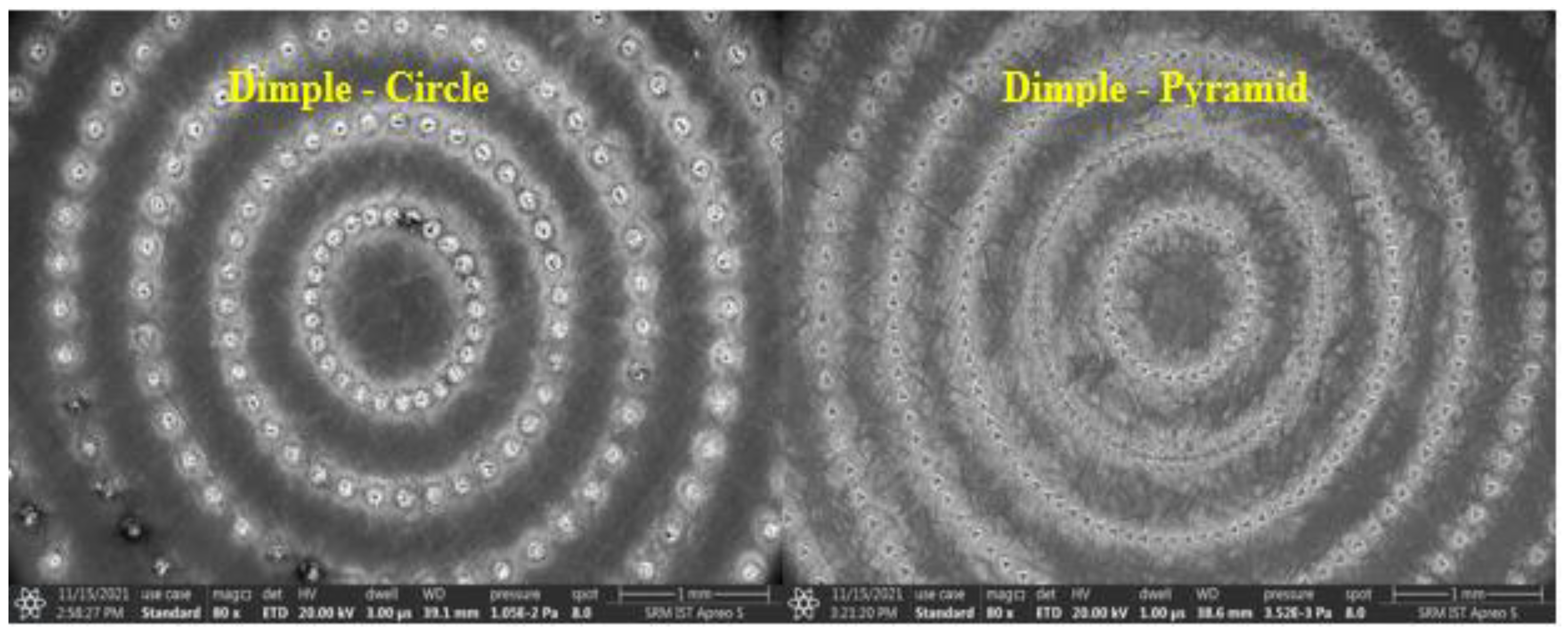
3.3. Micro-Textured Surface Characterization

Figure 7 depicts the morphological characteristics of the laser-textured silicon surface exhibiting various patterns, which resemble a succession of micrometer-scale hills with minor nano- and micro-scale characteristics. Additionally, a surface with a texture will improve visual features with circular, triangle dimples; also, it was discovered that the dimples overlapped, which caused more flashes when the pitch was closed and fewer flashes when the pitch increased. Due to the low thermal effect in laser texturization, which reduces the extrusion of a hill-like structure known as ripples on the surface, a precise shape (approx.) was discovered in this examination. Figure 8 illustrates the distinct dimple shapes that become more visible when the pitch between the dimples rises.
Figure 9 displays the composition of the constituents disclosed by EDX face-scanning studies before and after laser ablation. When textured surfaces are compared to untextured surfaces, it reveals the existence of Si, C, and O. Si is present in both surface elements consistently. However, because laser texturization was carried out in the surrounding environment, peaks connected to O and detected tiny peaks imply a limited C in the laser-textured surface region. The oxide layers are notably located over the surface. According to fiber laser texturization findings with high laser power (20 W), substantial melting and vaporization produce surface textures with ripples. The oxidation is caused mainly by temperature variation.

3.4. AFM Analysis

AFM is the superior technique used to assess the topography in nanoscale to analyze the features of the surfaces. AFM provides information about the surface profiles and the degree of material failure [18] to evaluate at the atomic level after the machining process. It promotes the deterioration of solar and semiconductor devices. The nano-morphology and AFM [19] observations of the sliced surfaces are used to evaluate the impact of AWJ parameters on the surface quality. The photographs obtained from AFM, which operated in the AM mode, are examined using WSxM, a programme developed by Microsoft Windows that was transcribed and used for scanning probe microscopy. Figure 10 demonstrated the 3D view of the laser-textured silicon samples in different patterns (dimple–circle and pyramid) where the texturing as a consequence of laser is influenced by the increase in temperature, which affects the developments in the surface modification due to melting, floating and re-solidification. It exposes the surface features consequence includes cracks, ripples, etc., which were specified with a contrast of gloaming due to the hydrodynamic effect [16]. It is influenced by temperature change, which impacts the initiation of surface modification which leads to pattern formation. Using AFM images with crests and valleys that may be analyzed for different dimple patterns, the surface roughness (Ra) of the textured and untextured surface and its variance of the surface waviness (RRms) data are computed.
The 3D surface imperfection photographs for the silicon specimen’s dimple pattern, are presented in Figure 11, where the wavelength is 1064 nm, the repetition rate is 40,000 pulses/second, and the pulse duration is 50 ns. For the circular and pyramidal surfaces with a 70 µm dimple texture, the average heights were 547 µm and 507 µm while the RMS roughness was 283 µm and 281 µm, respectively. Likewise, the 80 µm dimple pattern with a circle, pyramid and polygon exhibit an average height of 517 μm and 510 μm while the RMS roughness was 278 μm and 280 μm, respectively. The 90 µm dimple pattern for the circular and pyramid have RMS roughness of 279 μm, 280 μm and an average height of 518 µm and 515 µm, respectively. The highest peak and lowest root can determine the waviness by estimating the distance between the profound mountain and shallow valley. This waviness helps to have several reflections, increasing absorption length and improving solar efficiency.

3.5. Fractal Dimensional (D) Analysis

Numerous study works, some of which have noted fractal characteristics in surface topography, have found that fractal dimension (D) oriented examination of the surface generates more equitable and advantageous findings than traditional computation [20]. The peculiarities and imperfections of reality were inaccurately portrayed by classic and Euclidean geometry; Fractal geometry, however, provides a more accurate portrayal. Several methods based on fractional Brownian motion and box-counting fractal dimension are applied to determine the stochastic properties of the complex, unquantifiable designs on the silicon substrate. In this investigation, PSD, based on the fractional Brownian method, is used. The gradient of the height contours is averaged, and FD is determined using the equation FD = 7/2 + α/2. The multifractal offers quantitative properties that describe the scale aspects of geometric properties. The surface fractal dimension (2 < FD < 3) and the profile fractal dimension (1 < FD < 2) are computed. According to the studies above, the more significant fractal dimension number, between 1 and 2, is more complicated. Typically, the smoother and “coarser” the texture, the significantly larger the fractal dimension. The flaws in the measured surface observed reveal that the surface’s complexity changes from 1 to 2, which elaborate the non-uniformity of the surface profile. The quality of the curves with fractal features can be demonstrated by,
N   ( T ) = T D
( i . e . , )   L   ( T ) = N   ( T ) = T 2 D
As a result, D may be calculated
D = l o g   N   ( T ) / l o g   ( 1 / T )
D = l o g   N   ( T ) / l o g   ( T )  
where: T—Dimension of the evaluation scale; N (T)—Total amount of observations taken; L (T)—Overall length of the associated curve; D—Dimensions of Fractals.
The evaluation of D is accomplished by displaying the slope between computed values (log (P)) vs. step sizes (log (S)), as displayed in Figure 12, with a micro-textured (70 µm) substrate surface with circular pattern. As a result of the swelling consequences brought on by the abrupt rise in surface temperature during texturing, the AFM photograph reveals that an embankment-like structure was discovered on the top face of the textured surface, which is not present in the untextured surface.
The D of the single crystal silicon slice shows that circular dimple-textured surfaces generated the most detailed profile in sizes of 70 µm (D = 1.833) when looking at the micro-textured pleomorphic profoundly different dimple patterns such as a circle and pyramid with varied sizes of 70 µm, 80 µm, and 90 µm. The highest D values, however, are displayed by the 80 µm and 90 µm pyramid-textured surfaces (D = 1.822 and 1.821, respectively). The texture with the following medium D values: 70 µm pyramid (1.793), 80 µm circular (1.797), and 90 m pyramid (1.793) (1.806). The unique circular design at 90 µm had the lowest D values, measuring 1.777. According to the observations, different dimple patterns vary in the fractal size range and surface waviness. This means that the remaining designs are rougher than the circularly dimpled patterns (70 µm), which are grimmer still. The 90 µm and 80 µm pyramid dimples were found to have more excellent fractal dimensions and coarser surfaces than the circular design. According to the study, using a fiber laser to irradiate a surface to produce a 70 µm circular dimple texture increased surface changes and roughness by about 3.5%, as opposed to 80 µm and 90 µm by 1.5%. We also identified that a circular depression of 70 m assures a 2.18% improvement to the surface’s pyramid pattern. It displays an enhancement of 4% FD compared to circular dimples and 1.95% FD and roughness compared to other dimples for a 90 µm textured surface. It also shows higher fractal dimensions with higher roughness for an 80 µm pyramid pattern with an increase of 1.86% compared to circular dimples of 1.97%.

3.6. Effect of Absorption and Reflectance without Surface Texturization

The trajectory of the light rays is increased by modifying the surface geometry, which multiplies the internal reflections and piles up the absorption. Those materials encompassing parasitic Fresnel reflection had a negative effect in the conversion of power [21]. By controlling the surface quality to raise the number of reflection and absorption cycles, it is possible to increase the absorptivity of both metallic and nonmetallic materials [22]. Surface features contribute to an increase in the light absorption by the substrate by modifying the contact area, which in turn enhances the number of reflections and helps aggregate absorbance by prolonging the light path. Laser-texturing is utilized to modify the sliced silicon surface with different patterns that enhance the solar device performance and also the sliced bare surface with distinct abrasives mesh sizes are evaluated using a UV-VIS spectrophotometer (SHIMADZU, UV 3600 PLUS). Figure 13 shows the absorption for the sliced silicon with various abrasive mesh sizes of garnet combined with MWCNT by altering the slicing parameters between 200 nm and 1600 nm. The results of the examination show that surface characteristics support the absorption endorsed by photon flux due to multiplied internal reflections, specifically it is high between 200 nm and 1600 nm wavelength range for a coarse abrasive particle (approximately 0.4–0.8%) which is shown in Figure 13a. The nanoparticles (MWCNT) coupled with the #120 sieve’s moderate absorption rate (about 0.5%) and imperfect fractal patterns had a much less significant impact on absorption. Due to their flat surface and high surface polish, fine abrasives with #120 mesh (about 0.4–0.5%) had less effect on absorption than other abrasives, as shown in Figure 13a.
When examining the reflectance between the various surfaces sliced by distinct mesh sizes (Figure 13b, we observed high reflectance up to 400 nm wavelength and declined from 400–1100 nm), which suggested a high reflectivity percentage because of its varied surface texture, the analysis above shows that surface characteristic is essential for improving absorption in the 200–1000 nm spectral range.
The absorption and reflectance percentage of silicon in the wavelength range of 200–1600 nm is listed in Table 2. While comparing the absorption percentage, we revealed the coarseness of the particles due to the height variance of the surface irregularities influenced by the slicing parameters results in higher absorption (0.5–0.55%) Figure 13a, and found some of the sliced surfaces has less influence because of poor fractal features which are not limited with a specific scale range. From Figure 13b, the observation revealed that reflectance is low (15–25%) in the sliced silicon with coarse particles having rough surfaces, but the reflectance percentage is high (38–45%) when small particle size abrasives are used because of good surface quality.

3.7. Effect of Absorption and Reflectance with Surface Texturization

Figure 14 compares the absorption of micro-sized dimple-shaped features created by nanosecond laser machining at wavelengths between 200 and 1000 nm. For fiber laser texturization, the following operational parameters were used: a 50 ns pulse width, a 30 kHz laser frequency, a 7 µm laser beam diameter, a 60 W laser power, and a 226 mm object distance. Because internal reflection lengthens the path of the light in the textured workpiece surface endowed with Lambertian light-scattering and increases absorption, it has been found that increasing wavelength decreases absorption almost like an independent and dependent variable in a linear function [23]. This is because the textured work surface can reach the Yablonovitch light trapping limit. When the photon’s energy hits the flat surface and divides into absorbed and reflected energy, there is a possibility of varying light wave scattering in the textured substrate [24]. The textured surface boosts absorption by many reflections across the whole spectral range due to the pattern, size distribution, and top angle of the roughness formed in the surface. By examining, it is found that the textured silicon’s absorption rate alters the most significantly between the spectral region of 400 and 1000 nm (Figure 14). By comparing the absorptance percentages, it was found that the 70 m circular dimple (approximately 0.85%) had a high rate of absorption by multiple reflections due to the shape, density, and upper angle of the texture established in the surface. The circular dimples with various sizes had an absorption range of around 300 nm and 1000 nm (approximately). A more significant absorption rate is seen between the wavelengths of 200 nm and 1000 nm in pyramid-shaped dimples (around 2%), while just a tiny proportion is seen in dimples with a roughness of 90 m. According to the investigation, a surface having circular dimples can absorb more light than a surface with other dimple textures, regardless of size. However, a surface with pyramid-shaped dimples will absorb less energy as its size increases.
According to Figure 15, 90 μm circular dimples reflect light less than 70 μm and 80 μm dimple patterns, while 70 μm and 80 μm pyramid-shaped dimples reflect light less than 90 μm dimple textures. When comparing the pattern, the pyramid-textured surface decreases from 40% to 8%, and the circular dimple falls from 45% to 28%.
The absorption of a textured silicon substrate with different dimple shapes (circle and pyramid) and sizes (70 μm, 80 μm, 90 μm) in the wavelength range of 200–1600 nm are listed in Table 3. While comparing the absorption percentage of different dimple shapes, we revealed the pyramid-shaped dimple have results in higher absorption (1–2%), (1–1.5%), (0.8–1%) Figure 14, compared with the other dimple shapes (circular—0.55–0.85%, 0.60–0.80%, 0.70–1.15%) because of poor fractal features which are not limited with a specific scale range.
Likewise, the reflectance percentage of the micro-textured pattern with different shapes and sizes in the wavelength range of 200–1600 nm is listed in Table 3. From Figure 15, the observation revealed that reflectance is high (28–30%) in the 70 µm circular dimple. However, the reflectance percentage is low (8%) for the pyramid and also found to increase in reflectivity with its size because of its variations in surface modification. By comparing the three different shapes, we found circular dimples had low reflectivity when their size was large, and pyramids had high reflectance. The absorption level shows the effect of texture in the silicon surface with a long light trapping path and a high percentage of absorption compared with the flat surface, irrespective of their shapes. In reflectance, we noticed the vast differences compared with the flat sliced surface with a low percentage of reflectance because of the orderly arranged pattern and the angle provided for internal reflections, which helps for multiple internal reflections high, which enhances the absorption rate in the solar cell applications. The substantial number of pulses (>10) and the modest pitch between the dimples decreased absorption by up to 5–10% due to the silicon surface melting. The absorption between 300 and 500 nm wavelengths increased (10–15%) when the silicon slice’s surface was laser-textured. The interplay of light waves within the surface of the silicon surface with such “soft” ordered texturing improves light absorption.

4. Conclusions

Laser surface texturing on silicon was conducted using a nanosecond fiber laser to generate a uniform texture for the sliced silicon surface, increasing its anti-reflective property. Based on the investigation and analysis of the modified surface, the following inferences were drawn:
  • Uniform micro-texture with different shapes and sizes (circle and pyramid) were obtained in the order of incident laser wavelength by varying the important laser parameters.
  • The reflectivity of this textured surface (pyramid) was below 8% compared to untextured silicon at 40%, and absorptance increased from 1% to 2% in the wavelength range of 200 to 1000 nm.
  • After comparing the absorptivity and reflectivity graphs together, we found that the triangular dimple (pyramid) with decreased size (70 µm) showed a significant increase in absorptivity and a similarly significant decrease in reflectivity as compared to the other samples.
  • The complexity of the laser-textured surface with varied patterns (circle and pyramid) and untextured surfaces are quantified by fractal dimension (FD) analysis.
  • Despite being more expensive than other texturing methods, the process produces more critical and comprehensive results.

Author Contributions

S.O.N.R.: conceptualization, methodology, investigation, writing — original draft preparation, visualization and resources. S.P.: writing—reviewing and editing, supervision and validation. All authors have read and agreed to the published version of the manuscript.

Funding

This research received no external funding.

Data Availability Statement

Not applicable.

Conflicts of Interest

The authors declare no conflict of interest.

References

  1. Chand, M.; Mehta, A.; Sharma, R.; Ojha, V.N.; Nationa, K.P.C.; Marg, K.S.K. Roughness measurement using optical profiler with self-reference laser and stylus instrument—A comparative study. Indian J. Pure Appl. Phys. 2011, 49, 335–339. [Google Scholar]
  2. Radfar, B.; Es, F.; Nasser, H.; Akdemir, O.; Bek, A.; Turan, R. Effect of Laser Parameters and Post-Texturing Treatments on the Optical and Electrical Properties of Laser Textured c-Si Wafers. In Proceedings of the 8th International Conference on Crystalline Silicon Photovoltaics, Lausanne, Switzerland, 19–21 March 2018. [Google Scholar]
  3. Dasgupta, K.; Ray, S.; Mondal, A.; Gangopadhyay, U. Review on different front surface modification of both n+-p-p+ and p+-n-n+ C- Si solar cell. Mater. Today Proc. 2017, 4, 12698–12707. [Google Scholar] [CrossRef]
  4. Schwarz-Selinger, T.; Cahill, D.G.; Chen, S.-C.; Moon, S.-J.; Grigoropoulos, C.P. Micron-scale modifications of Si surface morphology by pulsed-laser texturing. Phys. Rev. B 2001, 64, 155323. [Google Scholar] [CrossRef]
  5. Lee, B.G.; Lin, Y.-T.; Sher, M.-J.; Mazur, E.; Branz, H.M. Light Trapping for Thin Silicon Solar Cells by Femtosecond Laser Texturing. In Proceedings of the 38th IEEE Photovoltaic Specialists Conference, Austin, TA, USA, 3–8 June 2012; pp. 001606–001608. [Google Scholar] [CrossRef]
  6. Basher, M.K.; Hossain, M.K.; Akand, M.A.R. Effect of surface texturization on minority carrier lifetime and photovoltaic performance of mono-crystalline silicon solar cell. Int. J. Light Electron Opt. 2019, 176, 93–101. [Google Scholar] [CrossRef]
  7. Bougoffa, A.; Trabelsi, A.; Zouari, A.; Dhahri, E. Analytical model of front texturization effect on silicon solar cell with porous silicon at the backside. Opt. Quantum Electron. 2016, 49, 16. [Google Scholar] [CrossRef]
  8. Demir, A.G.; Maressa, P.; Previtali, B. Fibre laser texturing for surface functionalization. Phys. Procedia 2013, 41, 759–768. [Google Scholar] [CrossRef] [Green Version]
  9. Dobrzański, L.A.; Drygała, A. Laser Application in Photovoltaics for Surface Texturization of Silicon and Front Electrode Deposition. Mater. Perform. Charact. 2019, 8, 20190061. [Google Scholar] [CrossRef]
  10. Sai, H.; Fujiwara, H.; Kondo, M.; Kanamori, Y. Enhancement of light trapping in thin-film hydrogenated microcrystalline Si solar cells using back reflectors with self-ordered dimple pattern. Appl. Phys. Lett. 2008, 93, 143501. [Google Scholar] [CrossRef]
  11. Eisenhauer, D.; Sai, H.; Matsui, T.; Koppel, G.; Rech, B.; Becker, C. Honeycomb micro-textures for light trapping in multi-crystalline silicon thin-film solar cells. Opt. Express 2018, 26, A498. [Google Scholar] [CrossRef]
  12. Nayak, B.K.; Iyengar, V.V.; Gupta, M.C. Efficient light trapping in silicon solar cells by ultrafast-laser-induced self-assembled micro/nano structures. Prog. Photovolt Res. Appl. 2011, 19, 631–639. [Google Scholar] [CrossRef]
  13. Vinčiūnas, A.; Indrišiūnas, S.; Voisiat, B.; Račiukaitis, G.; Šimkienė, I.; Suzanovičienė, R.; Rėza, A.; Mažeikienė, R. Effect of Laser Patterning on Properties of Crystalline Si Photovoltaic Cells and Substrates. J. Laser Micro/Nanoeng. 2013, 8, 244–252. [Google Scholar] [CrossRef] [Green Version]
  14. Prasad, K.N.; Syed, I.; Subbu, S.K. Laser dimple texturing—Applications, process, challenges, and recent developments: A review. Aust. J. Mech. Eng. 2019, 20, 316–331. [Google Scholar] [CrossRef]
  15. Farrokhi, H.; Zhou, W.; Zheng, H.Y.; Li, Z.L. Non-ablative texturing of silicon surface with a continuous wave fiber laser. Opt. Express 2012, 20, 23180–23185. [Google Scholar] [CrossRef]
  16. Vidhya, Y.E.B.; Vasa, N.J. Numerical and Experimental analysis of nano second laser induced surface textures for light trapping in a-Si thin film for solar cells. Mater. Res. Express 2018, 5, 066410. [Google Scholar] [CrossRef]
  17. Joshi, K.; Bhandarkar, U.; Samajdar, I.; Joshi, S.S. Micro-structural characterization of thermal damage on silicon wafers sliced using wire-EDM. J. Manuf. Sci. Eng. 2018, 140, 091001. [Google Scholar] [CrossRef]
  18. Guu, Y.H. AFM surface imaging of AISI D2 tool steel machined by the EDM process. Appl. Surf. Sci. 2005, 242, 245–250. [Google Scholar] [CrossRef]
  19. Prabhu, S.; Vinayagam, B.K. AFM investigation in grinding process with nanofluids using Taguchi analysis. Int. J. Adv. Manuf. Technol. 2011, 60, 149–160. [Google Scholar] [CrossRef]
  20. Fashina, A.; Adama, K.; Abdullah, L.; Ani, C.; Oyewole, O.; Asare, J.; Anye, V. Atomic force microscopy analysis of alkali textured silicon substrates for solar cell applications. Int. J. Phys. Res. 2017, 6, 13–17. [Google Scholar] [CrossRef] [Green Version]
  21. Brown, M.S.; Arnold, C.B. Fundamentals of laser-material interaction and application to Multi scale surface modification. Laser Precis. Micro Fabr. 2010, 135, 91–120. [Google Scholar]
  22. Niu, C.; Zhu, T.; Lv, Y. Influence of Surface Morphology on Absorptivity of Light-Absorbing Materials. Int. J. Photoenergy 2019, 2019, 1476217. [Google Scholar] [CrossRef]
  23. Mahdieh, M.H.; Sobhani, M. Experimental Study of Nano-Structure and Optical Properties of Polished Silicon Irradiated by Nanosecond Nd:YAG Laser Beam. In Proceedings of the 15th International Conference on Laser Aided Plasma Diagnostics, Jeju, Republic of Korea, 13–19 October 2011. [Google Scholar]
  24. Raj, S.O.N.; Prabhu, S. Investigation on Slicing Behavior of Single Crystal Silicon Wafer in AWJM and Influence of Micro Dimple Textured Surface for Solar Applications. Silicon 2020, 13, 4481–4499. [Google Scholar] [CrossRef]
Figure 1. AWJ sliced single-crystal silicon.
Lubricants 11 00015 g001
Figure 2. Schematic diagram of different dimple-textured pattern (circle, triangle).
Lubricants 11 00015 g002
Figure 3. Dimple-textured silicon samples with different pattern.
Lubricants 11 00015 g003
Figure 4. 3D images of textured sample surface texturing.
Lubricants 11 00015 g004
Figure 5. XRD peaks of the untextured and laser-textured (70 µm) silicon surface.
Lubricants 11 00015 g005
Figure 6. Raman peaks of the untextured and micro-textured silicon surface.
Lubricants 11 00015 g006
Figure 7. SEM image of fiber laser 70 µm dimple-textured silicon surface.
Lubricants 11 00015 g007
Figure 8. SEM images of 70 µm circular and pyramid dimple-textured surface.
Lubricants 11 00015 g008
Figure 9. Constituent of elements before and after laser texturization, from EDS spectrum analysis.
Lubricants 11 00015 g009
Figure 10. 3D view of the silicon laser-textured samples with patterns (dimple–circle and pyramid).
Lubricants 11 00015 g010
Figure 11. AFM image for laser-textured silicon samples in different patterns (dimple (70 µm)–circle, pyramid.
Lubricants 11 00015 g011
Figure 12. FD analysis of textured silicon surface, 70 µm, D = 1.833 (circular).
Lubricants 11 00015 g012
Figure 13. Untextured silicon’s absorbance and reflectance.
Lubricants 11 00015 g013
Figure 14. Comparison of the micro-textured pattern’s absorbance range concerning the size.
Lubricants 11 00015 g014
Figure 15. Comparison of the micro-textured pattern’s reflectance range concerning the size.
Lubricants 11 00015 g015
Table 1. Laser micro-texturing parameters.
Micro-Texturing ParametersUnitDimple 70 µmDimple 80 µmDimple 90 µm
Wavelengthnm106410641064
Pulse widthns5010050
Focal lengthmm226226226
FrequencykHz405060
Pitchµm708090
Laser pulse energymJ0.50.80.5
Laser PowerW202020
No. of Pulses 51010
Table 2. Absorption and reflectance percentage of untextured silicon.
Absorption % (Approx.)Reflectance % (Approx.)
A1P10.4–0.5R1P135–40
A1C10.4–0.45R1C138–45
A2P20.45–0.5R2P230–38
A2C20.6–0.8R2C215–25
A3P30.45–0.55R3P330–35
A3C30.5–0.55R3C330–35
Table 3. Absorption and reflectance percentage of the micro-textured pattern with different sizes.
Dimple PatternAbsorption % (Approx.)Reflectance % (Approx.)
70 µm80 µm90 µm70 µm80 µm90 µm
Circular0.55–0.850.60–0.800.70–1.1528–3025–2818–20
Pyramid1–21–1.50.8–181220
Disclaimer/Publisher’s Note: The statements, opinions and data contained in all publications are solely those of the individual author(s) and contributor(s) and not of MDPI and/or the editor(s). MDPI and/or the editor(s) disclaim responsibility for any injury to people or property resulting from any ideas, methods, instructions or products referred to in the content.

