Article

Molecular Dynamics Analysis of Adhesive Forces between Silicon Wafer and Substrate in Microarray Adhesion

1
College of Mechanical and Electrical Engineering, Wenzhou University, Wenzhou 325035, China
2
Technology Science and Technology Research Institute, Xinchang Zhejiang University, Shaoxing 312500, China
*
Author to whom correspondence should be addressed.
Lubricants 2024, 12(6), 183; https://doi.org/10.3390/lubricants12060183
Submission received: 16 March 2024 / Revised: 10 May 2024 / Accepted: 17 May 2024 / Published: 21 May 2024

Abstract

:
With the development of the electronics industry, the requirements for chips are getting higher and higher, and thinner and thinner wafers are needed to meet the processing of chips. In this study, a model of the adhesion state of semiconductor wafers in the stacking–clamping process based on microarray adsorption was established, the composition adhesion was discussed, the microarrays of different materials and pressures were experimentally studied, and a molecular dynamics model was established. The molecular dynamics analysis showed that the adhesion force was only related to the type of atom, and the applied pressure did not change the adhesion force. According to the simulation results, the tangential adhesion between the metal and the wafer is greater than that between the ceramic and the wafer, the adsorption force between the aluminum–magnesium alloy and the silicon wafer is shown in the normal direction, and the repulsion force between other materials and the silicon wafer is shown in the normal direction. During the pressure process, the metal is in the elastic deformation stage between the metal and the wafer, the wafer is plastically deformed in the silicon carbide ceramic and wafer, and the wafer is elastically deformed in the alumina ceramic and wafer. In this paper, the adhesion between the substrate and the wafer is studied, a method of constructing microarrays to enhance adhesion is proposed, and the tangential deformation of the array unit under pressure is studied, which provides theoretical support for increasing the adhesion by constructing microarrays.

1. Introduction

Semiconductor refers to materials with electrical conductivity between conductors and insulators at room temperature. The conductivity of semiconductors can be controlled by voltage, light, pressure, and temperature. Semiconductor wafers are widely used in semiconductor applications, and to improve the processing efficiency in semiconductor devices, large-sized wafers are necessary. Larger wafer sizes enable the production of more components, thereby reducing costs [1]. Simultaneously, wafers need to be thinned to produce high-performance devices. The mainstream methods for manufacturing ultra-thin wafers are mechanical grinding and polishing [2,3,4,5,6].
In the current thinning processes, double-sided grinding is favored for its high removal rate, high flatness, high parallelism, and symmetrical stress introduction [7]. It has been applied in processing various planar components. In double-sided grinding, the planetary wheel serves as the primary clamping mechanism. However, challenges arise as the thickness of the planetary wheel needs to be smaller than that of the silicon wafer, leading to issues related to the rigidity and strength of the planetary wheel [8]. Traditional mechanical fixtures were initially used for clamping, but they are rarely employed nowadays.
In the early 20th century, G.A. Wardly and others proposed a novel silicon wafer clamping tool—electrostatic suction cup [9]. This approach fixes the silicon wafer through electrostatic adsorption, distributing the adhesive force uniformly across the wafer surface, preventing warping or deformation. However, electrostatic chucks have limitations, such as weaker force compared to vacuum chucks, dust adherence to the top of chuck pins, and deformation during chucking. Atsunobu and others developed a new non-deforming chucking technology that does not rely on electrostatic or vacuum forces and does not damage the contact surface [10]. Yoshitomi developed a frozen pin chuck system, studying a non-deforming clamping process for thin substrates. For a wafer with a diameter of 300 mm, thickness of 1.2 mm, and warpage of 100 μm, the fixed strength in the shear direction exceeded 110 kPa [11]. The maximum deformation using the chucking process was only 10 μm. A correction processing system was developed to address the deformation caused by the attractive force of the bending moment, allowing grinding and polishing while using frozen pin chucking. This system possesses non-deforming clamping capabilities, suppressing the deformation of initially warped substrates by more than 90% and enhancing locking force [12].
However, these clamping methods are not suitable for use during grinding. Presently, the main semiconductor wafer clamping methods include vacuum adsorption [13], paraffin bonding [14], planetary wheel clamping [15], and wax-free adsorption [16]. Vacuum adsorption can lead to localized deformation of the workpiece, while paraffin bonding is cumbersome and inefficient. Planetary wheel clamping demands high material requirements for the fixture, and wax-free adsorption is unable to adhere to ultra-thin workpieces. Additionally, Chen and others proposed a stacked clamping method, establishing a numerical model based on fractal theory and experimentally verifying the model’s effectiveness [17]. They also experimentally validated the polishing performance of stacked clamping [18] and studied the failure mode of limit pieces, attributing it to edge cutting causing the fracture of limit pieces [19]. The clamping mechanism of stacked clamping was investigated, analyzing the adhesive forces between the substrate and the workpiece. It was concluded that under wet conditions, suction primarily manifests as capillary force, while under dry conditions, it exhibits van der Waals force. Wet capillary force was experimentally verified, but no research was conducted on suction under dry conditions. Delrio built a framework to study the interfacial forces that exist during adhesion, studied the adhesion results on horizontal and vertical surfaces, and studied the effect of contact pressure on adhesion, and reduced the adhesion force by reducing the actual contact area in different ways [20].
This article employs molecular dynamics methods to investigate the adhesive forces between silicon wafers and substrates in a stacked clamping fixture. By establishing a micro-contact model, the study explores van der Waals forces and mean square displacement (MSD) between the contact surfaces under static conditions. The analysis delves into the adhesive forces and molecular diffusion levels in the normal and tangential directions between the substrate and the silicon wafer. Applying pressure to harder materials in both the substrate and silicon wafer, the study analyzes the changes in adhesive forces, MSD, and stress–strain during this process. The research reveals that under static conditions, the tangential adhesive forces for the magnesium–aluminum alloy substrate–silicon wafer and iron–carbon alloy substrate–silicon wafer are greater than those for the aluminum oxide ceramic substrate–silicon wafer and the silicon carbide ceramic substrate–silicon wafer. The normal adhesive force for the aluminum–magnesium alloy substrate-silicon wafer is attractive, while for other combinations, it is repulsive. During compression, the magnitude of adhesive forces is independent of pressure, being influenced by the type of atoms and atomic distances. Additionally, during this process, the magnesium–aluminum alloy substrate and iron–carbon alloy substrate consistently undergo elastic deformation in the tangential direction.

2. Model

Molecular dynamics simulations were performed using the large-scale atomic/molecular massively parallel simulator (LAMMPS) [21]. The visualization of simulation trajectories was achieved through the open visualization tool (OVITO) [22]. For the silicon wafer, a square region measuring 100 nm by 100 nm was established. An uneven and rough surface was generated using a fractal function, and this surface was applied to create a silicon wafer with a roughness (Ra) of 10 nm. Additionally, uniform surfaces with a roughness (Ra) of 1 nm were generated using sine functions for the silicon carbide ceramic, the aluminum oxide ceramic, the magnesium–aluminum alloy, and the iron–carbon alloy.
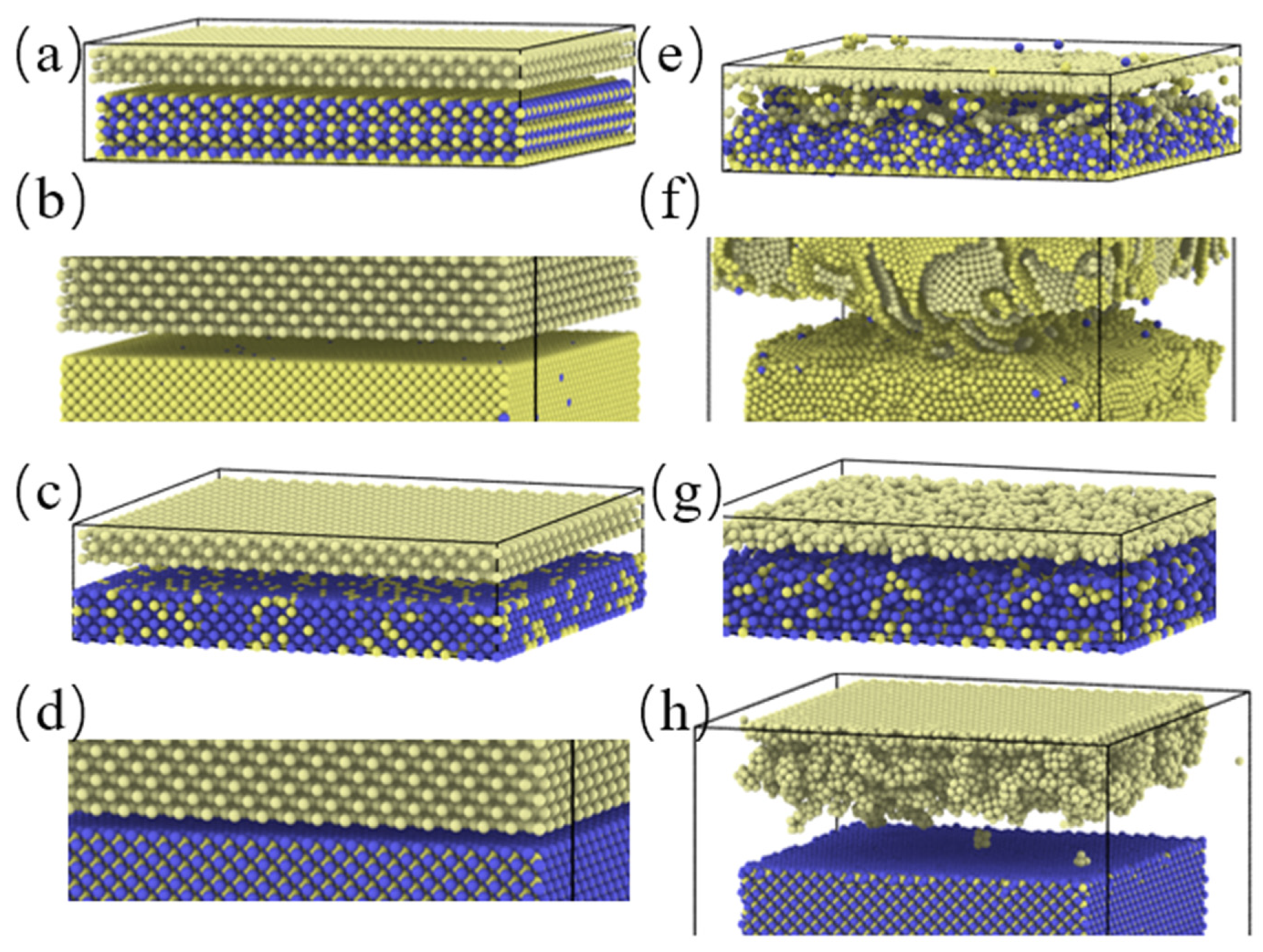
Figure 1 depicts the MD (molecular dynamics) model and atomic crystal structure of the adhesive process between a silicon wafer and different material substrates under static conditions. The substrate model includes two components: the silicon wafer and various material substrates. The substrate is positioned above, and the silicon wafer is positioned below. Both are divided into three regions: the boundary layer, the constant-temperature layer, and the Newtonian layer. From top to bottom, these include the substrate fixed layer, substrate constant-temperature layer, substrate Newtonian layer, gap, silicon wafer Newtonian layer, silicon wafer constant-temperature layer, and silicon wafer-fixed layer. Due to the small distance of adhesive force action and to accelerate simulation speed, the model has been simplified.
The atoms in the boundary layer are utilized to maintain the overall stability of the system, preventing slippage of the workpiece. Atoms in the constant-temperature layer dissipate heat during the adhesive process. Simultaneously, the kinetic energy of the atoms is adjusted at each simulation step, maintaining the average temperature at 300 K. The remaining atoms constitute the Newtonian layer. At the same time, the simulation system is kept dry to avoid the influence of temperature and water vapor on the simulation results.
During the simulation process, the interaction between silicon atoms in the silicon wafer is described using the Tersoff potential [23]. For the substrate, the Tersoff potential is employed to describe silicon carbide [24], while the COMB3 potential function is used for aluminum oxide [25]. Iron [26] and magnesium–aluminum alloy [27] are described using a modified embedded atom method. The non-bonded interactions between the silicon wafer and the substrate are represented by the Leonard–Jones potential, as shown in Equation (1) [28,29].
V L J = 4 ε [ ( σ r ) 12 ( σ r ) 6 ]
In the equation, r represents the distance between simulated atomic particles, ε is the depth of the potential well, and σ is the finite distance at which the atomic potential becomes zero. The relevant parameters for the atoms are shown in Table 1.
We use the Lorentz–Betello law to calculate the sum parameters between atoms ε and σ . The Lorentz rule was proposed by Lorentz in 1881 and is still theoretically valid for rigid systems [29]:
σ = σ i i + σ j j 2
Betlot’s rule definition:
ε ij = ε ii ε jj
In the LJ potential function, the force between atoms is short-range adsorption and long-range repulsion, and the lowest point of LJ potential energy is rmin = 21/6 σ, and r < rmin is the repulsion force and r > rmin is the adsorption force. In order to verify the range of the LJ potential function, a model of the adsorption force between the two groups of materials is established when the distance between the two sets of substrate materials and the silicon wafer is different, the model is shown in Figure 2.
The selection of boundary conditions plays a crucial role in simulations, and for static simulations, periodic boundary conditions were chosen. Various methods can be employed for optimizing atomic structures, and in this study, the conjugate gradient (CG) method was chosen for energy optimization. This algorithm offers advantages such as stepwise convergence, low memory requirements, high stability, and independence from external factors.
At the beginning of the simulation, it is necessary to determine the distance between the silicon wafer and the substrate, ensuring that the model does not experience significant repulsion due to too small atomic distances, leading to large initial velocities and atoms flying out of the boundaries. The motion equations between them were solved with a time step of 1 fs. The canonical ensemble (NVT) ensemble is used where the total energy within the system remains constant, while the individual energy components undergo changes. The initial and final temperatures were set to 300 K, mitigating the influence of temperature variations on the system. Once the various energies within the system reached a stable state, the simulation achieved equilibrium.
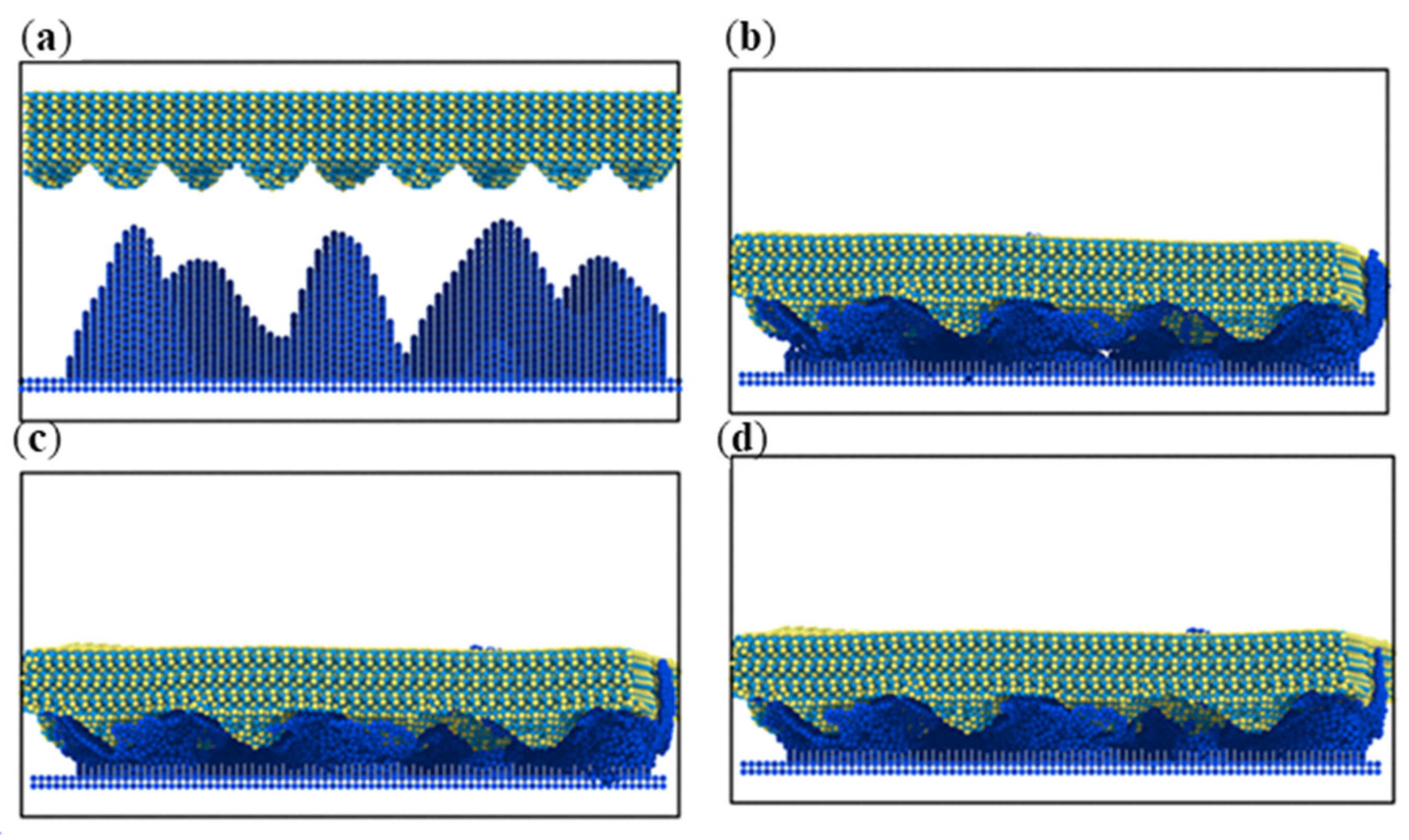
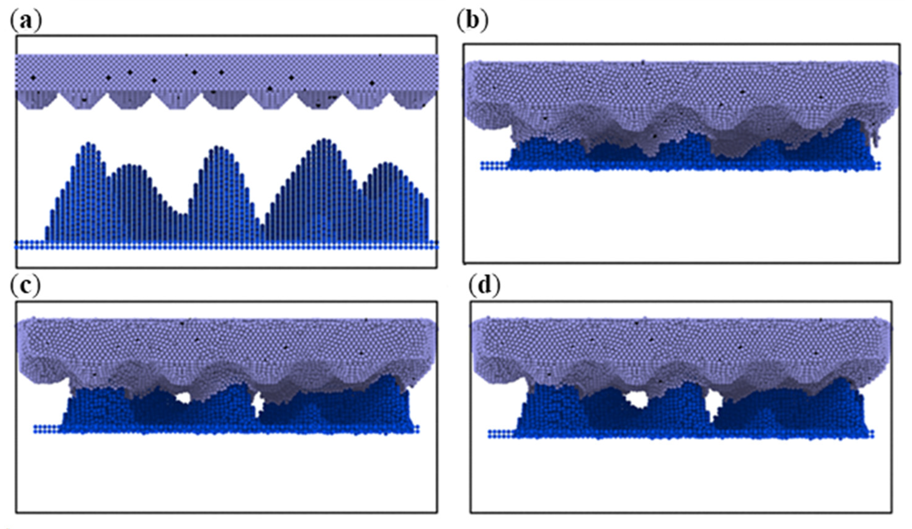
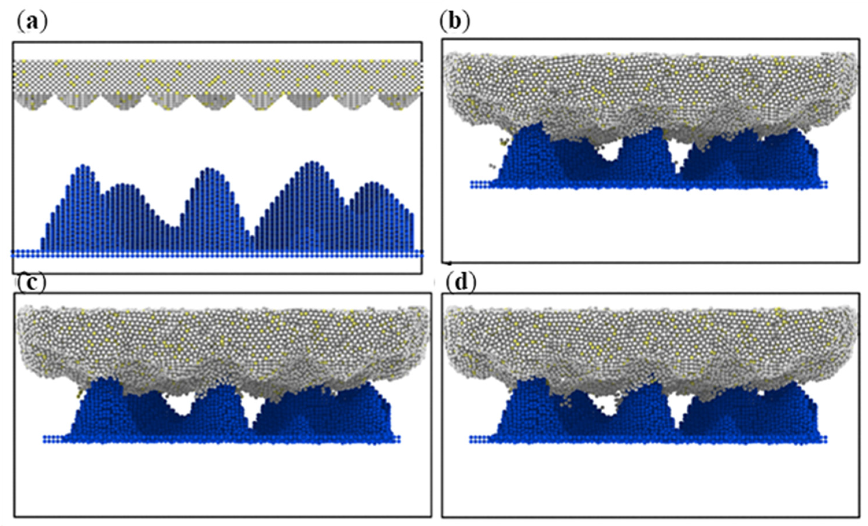
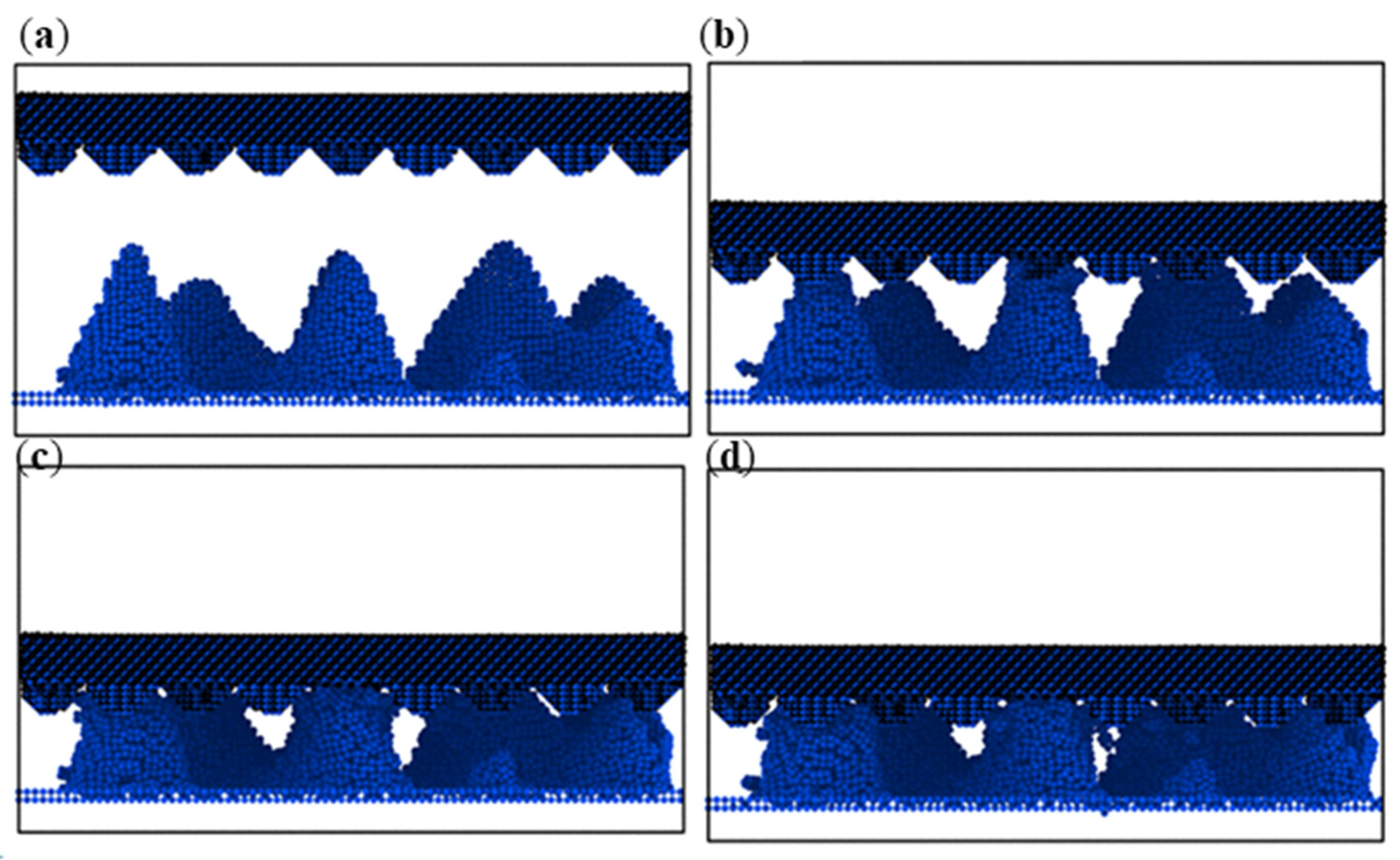
Figure 3, Figure 4, Figure 5 and Figure 6 illustrate the crystal structures during the dynamic simulation process, which is essentially similar to the static simulation. The difference lies in the dynamic simulation where the relatively hard materials in the silicon wafer and substrate are set as rigid bodies. When set as rigid bodies, the entire material is treated as a single entity, and the interactions between rigid body atoms are ignored during the simulation. The interactions between other atoms and the material layering remain the same as in the static conditions. Non-periodic boundary conditions were chosen in the X and Y directions, meaning that the boundary positions would change with the movement of the outermost layer atoms during the simulation.
The compression simulation is carried out in two steps. In the first step, acceleration is applied to the rigid body, causing contact between the silicon wafer and the substrate. After contact is established, the velocity of the rigid body is canceled and set to zero. In the second step, when pressure is applied to the rigid body, the rigid body will obtain the corresponding acceleration; when the applied pressure exerts pressure on each atom in the rigid body, all atoms are subjected to pressure and experience the applied pressure value, at the same time; when different atoms in the rigid body have different atomic masses, different forces need to be applied to different atoms to produce the same acceleration; the pressures exerted by all atoms involved in the compression are 0.1 MPa, 0.2 MPa, and 0.3 MPa, respectively. After calculation, the rigid body is stopped after moving 25 Å.
The mechanical properties were simulated in the LAMMPS software (version 8Feb2023-MPI) based on the applied load and deformation direction. The initial length was determined based on the size of the box. The strain equation was then applied to the stretched structure, determining its instantaneous length and establishing a stress–strain curve to determine the strain generated in the atomic structure. In the presence of load, a calculation program can be used to determine the value of structural strain.
During this process, as the contact area between the rigid body and the Newtonian layer changes, the load on the Newtonian layer also varies. According to Hooke’s law, strain in a solid is proportional to the applied stress and should be within the elastic limit of the material. The yield point of the material is defined as the point at which it begins to undergo plastic deformation. Permanent plastic deformation occurs beyond the yield point. The stress–strain curve for the Newtonian layer atoms, changes in adhesive forces between Newtonian layer atoms and rigid body atoms, and the mean square displacement (MSD)—a measure of the deviation of particle positions from their reference positions over time—were output during this process. In the simulation process, the changes of the stress–strain curve in the X and Y axes and the change rates of adhesion and MSD in the X-axis, Y-axis and Z-axis were calculated by the program, and the adhesion force and MSD were converted into normal and tangential changes.

3. Results and Discussion

3.1. Simulation under Static Conditions

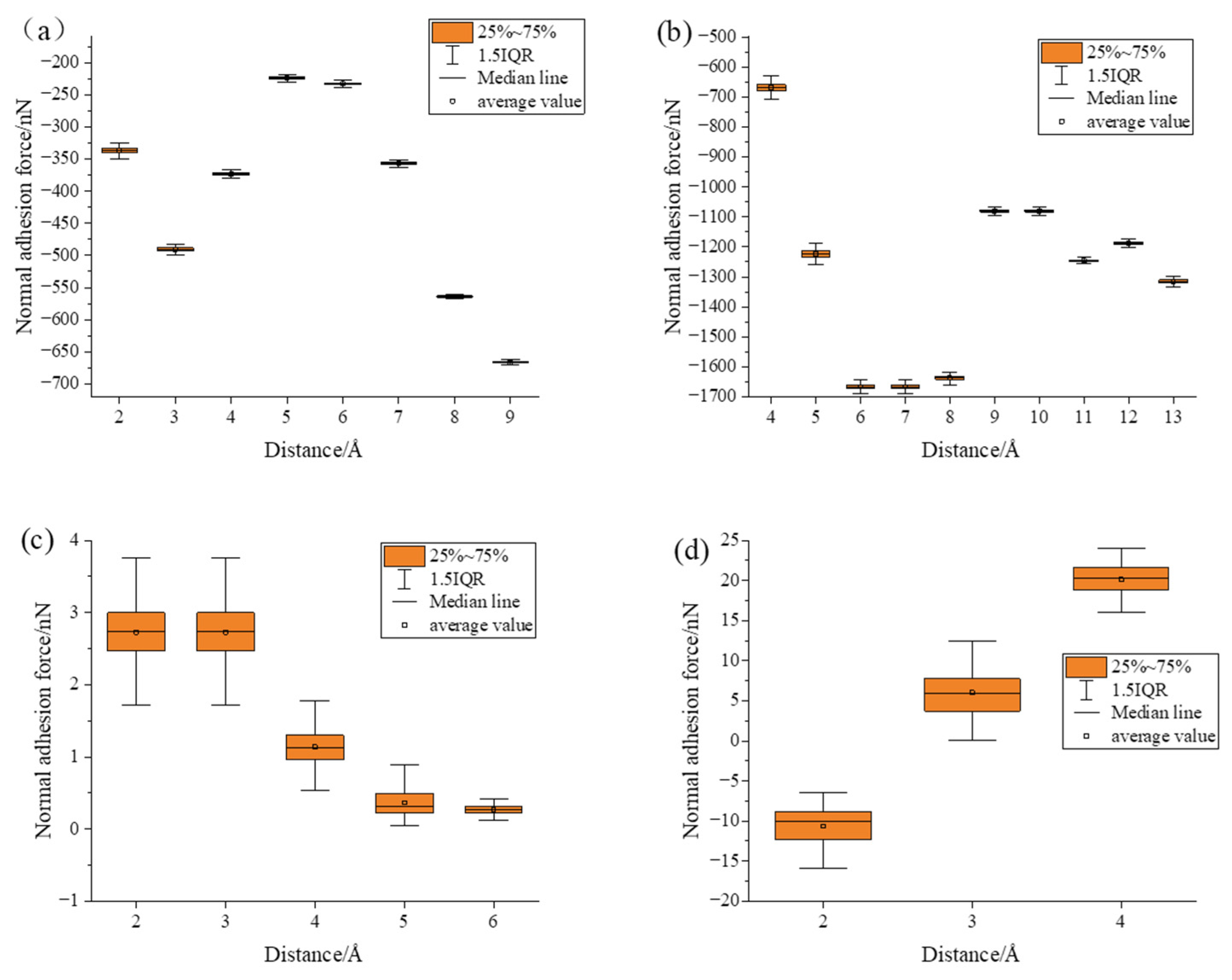
Figure 7 shows the normal adhesion between groups of materials at different distances, in silicon wafers and alumina ceramics and silicon wafers and iron–carbon alloys, the adhesion force generated between atoms is a repulsive force that causes the atoms to move more and more atoms move, so the distance that can produce the force is farther, and the final force is also larger. In silicon wafers and aluminum–magnesium alloys and silicon wafers and silicon carbide ceramics, the atoms move less amplitude, and the final force is limited, and the distance at which the force can be generated is smaller. In the simulation results of each group, the overall normal adhesion of silicon wafers and alumina ceramics to silicon wafers and iron–carbon alloys is repulsion, and the other groups of atoms in the group are adsorption forces and have maximum normal adhesion at different distances.
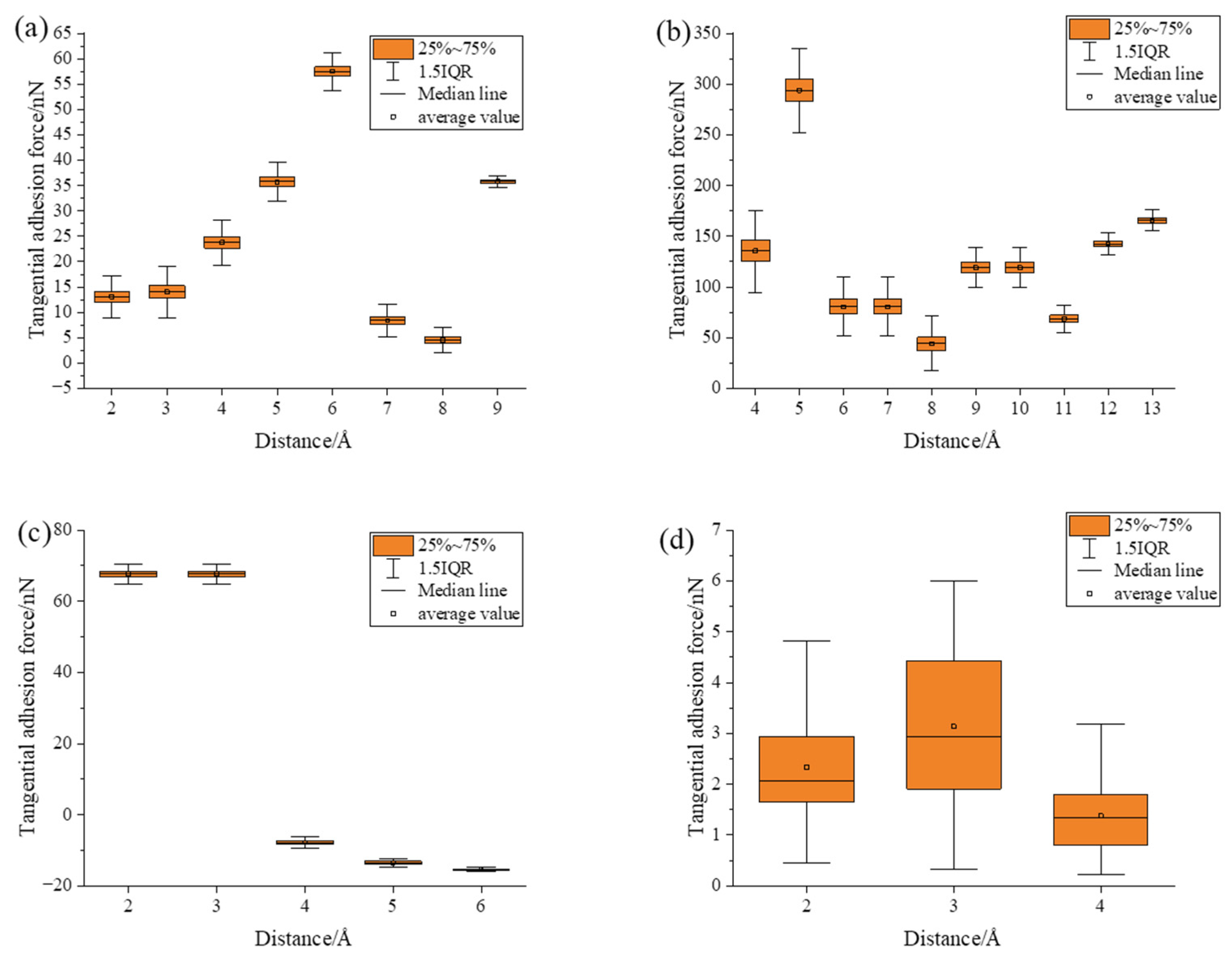
Figure 8 is the tangential adhesion between the groups of materials at different distances. The tangential adhesion between the groups is suction, silicon wafers and alumina ceramics, and silicon wafers and iron–carbon alloys, in the tangential direction is the repulsion force that causes more atoms to participate in the adhesion, in the tangential direction, compared with the silicon wafer and the aluminum–magnesium alloy and the silicon wafer and the silicon carbide ceramic, the atom pairs involved in the adsorption are more, so the normal adsorption force is larger, when comparing the tangential adhesion between ceramic materials and metal materials and silicon wafers, The adsorption force between the iron–carbon alloy and the silicon wafer is greater than that between the alumina ceramic and the silicon wafer, and the adsorption force between the aluminum–magnesium alloy and the silicon wafer is greater than that between the silicon carbide ceramic and the silicon wafer.
Figure 9 shows the variation of adhesion force and mean square displacement (MSD) between various material substrates and silicon wafers under static conditions. A comprehensive analysis reveals that silicon carbide and alumina ceramics reach a stable state in a relatively similar timeframe, closely followed by aluminum–magnesium alloys and iron–carbon alloys.
Figure 9a,b, respectively, represent the tangential and normal adhesion forces between the silicon wafers and substrates. It was found that silicon carbide and alumina ceramics reach stability quicker, while aluminum–magnesium and iron–carbon alloys take longer to stabilize. Tangentially, the adhesion force between the silicon carbide substrate and the silicon wafer is the lowest at 0.18 nN. Alumina ceramics and aluminum–magnesium alloys have similar adhesion forces at equilibrium, at 6.25 nN and 6.1 nN, respectively, while iron–carbon alloys exhibit the highest adhesion force at 10.8 nN, with the largest fluctuations upon reaching equilibrium. In the normal direction, silicon carbide shows the lowest adhesion force at 1.4 nN. The adhesion force for aluminum–magnesium alloys is 28.3 nN, while alumina ceramics and iron–carbon alloys exhibit repulsive forces at 110.3 nN and 220.6 nN, respectively.
Figure 9c,d show the MSD changes in the tangential and normal directions of atoms in the system during the simulation. In the tangential direction, the MSD changes for silicon carbide ceramics, alumina ceramics, aluminum–magnesium alloys, and iron–carbon alloys are 3.8 Å, 7.3 Å, 5.1 Å, and 0.7 Å, respectively. In the normal direction, the changes are 0.19 Å for silicon carbide, 0.47 Å for alumina ceramics, 1.46 Å for aluminum–magnesium alloys, and 3.88 Å for iron–carbon alloys.
From the results after simulation in Figure 1, it can be seen that in the alumina ceramic substrate–silicon wafer pair, the main changes occur in the silicon atoms within the silicon wafer, while the alumina ceramic substrate does not deform significantly. Both alumina ceramics and silicon wafers bond through covalent bonds. However, in alumina, oxygen atoms form a hexagonal close-packed structure, and aluminum atoms form an octahedral network structure. Compared to the close packing in silicon, the structure of alumina ceramics is more stable and less prone to deformation. In the iron–carbon and aluminum–magnesium alloy substrates, the materials are bonded by metallic bonds, which are less stable than the covalent bonds in silicon wafers, leading to larger deformations in the atomic model. This results in more atoms participating in the formation of adhesion forces and stronger van der Waals adsorption between the materials. The more atoms that move tangentially, the less space there is for movement, resulting in greater displacement in the normal direction. Since silicon carbide and silicon both have covalent bonds and closely packed lattice types, both substrates and wafers deform, but the deformation is minor due to their similar stability. The degree of atomic deformation explains the magnitude of adhesion forces. In Figure 1e,g, the deformation levels of silicon and aluminum–magnesium alloys are similar, so their tangential adhesion forces are nearly identical. In the normal direction, since the main deformations occur in the silicon wafer and aluminum–magnesium alloy, and alumina is flat, there are no intersections between alumina and silicon atoms in the normal direction. Therefore, all atomic pairs exhibit repulsive forces, with no attractive atomic pairs formed. In contrast, there are intersections between the aluminum–magnesium alloy and silicon wafer in the normal direction, resulting in both attractive and repulsive atomic pairs, ultimately manifesting as adhesive forces. In Figure 1f, the largest movement of atoms results in the strongest tangential adhesive force. In the normal direction, the excessive movement of iron atoms leads to repulsion with the underlying silicon atoms, ultimately resulting in a repulsive force. In Figure 1h, since silicon carbide and silicon wafers undergo the least deformation, they exhibit the lowest adhesive forces both tangentially and normally.

3.2. Simulation with Different Loads

Experiments applying different loads were conducted between various material substrates and silicon wafers, with pressures of 0.1 MPa, 0.2 MPa, and 0.3 MPa. During the simulation, alumina ceramics, aluminum–magnesium alloys, and iron–carbon alloys all reached the preset compression distances according to the program settings. Between silicon carbide ceramics and silicon wafers, the compression distances at 0.1 MPa, 0.2 MPa, and 0.3 MPa were 12.67 Å, 22.9 Å, and 24.8 Å, respectively.
Analysis from Figure 3, Figure 4, Figure 5 and Figure 6 indicates that during the compression process, the different bonding methods and lattice types of the materials, along with the potential for new bonds forming when atoms come into contact, all influence the simulation results. In the alumina ceramic substrate–silicon wafer pair, the hardness of alumina ceramic is much greater than that of the silicon wafer. When compressed the same distance, the silicon wafer deforms more. After energy minimization and relaxation, alumina ceramic deforms, creating gaps at the boundaries. Silicon atoms from the wafer entering these gaps also affect the simulation results. In the iron–carbon alloy substrate–silicon wafer pair, new bonds form when iron atoms come into contact with silicon atoms. The lower the pressure, the longer the simulation takes, resulting in more new bonds. In the aluminum–magnesium alloy substrate–silicon wafer pair, the aluminum–magnesium alloy undergoes significant deformation after energy minimization and relaxation, reducing the distance between the peaks and troughs of the sinusoidal surface waves. For the silicon carbide ceramic substrate–silicon wafer pair, since silicon carbide ceramics and silicon wafers have similar lattice types and bonding methods, and their material hardness is relatively close, the deformation is limited when the pressure is insufficient. The impact of these factors on the specific results will be explained in the detailed analysis of the results.
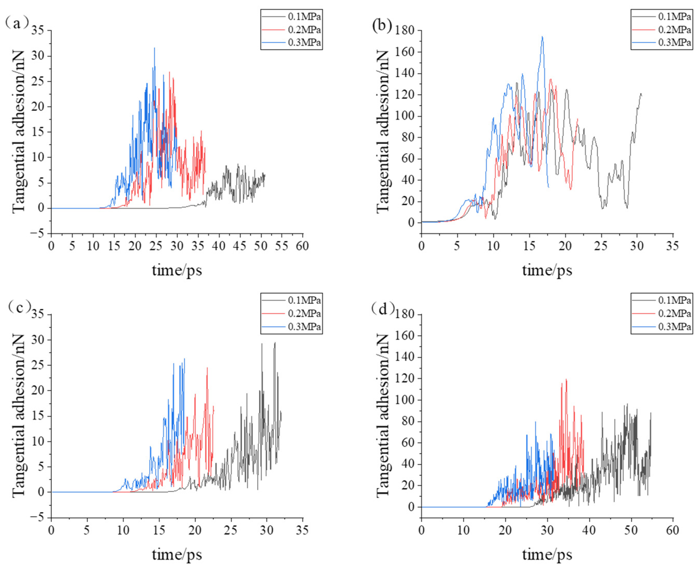
Figure 10 shows the tangential adhesion force changes between different material substrates and silicon wafers under applied pressure. Figure 10a–d correspond to the adhesion forces between silicon carbide ceramics, iron–carbon alloys, aluminum–magnesium alloys, and alumina ceramics with silicon wafers, respectively. After contact between the substrate and silicon wafer, adhesion forces are generated. As the contact deepens, the fluctuations in adhesion force increase. Additionally, different applied pressures result in different acceleration rates for the atoms, leading to different start and end times for the contact process. As contact progresses, the changes and fluctuations in the adhesion force between the substrate and silicon wafer become similar. The adhesion forces of iron–carbon alloys and alumina ceramics are greater than those of silicon carbide ceramics and aluminum–magnesium alloys. At 0.1 MPa pressure, since the contact depth of silicon carbide does not reach the preset distance, its adhesion force is similar to that in the early stages of contact at 0.2 MPa and 0.3 MPa. The adhesion force of iron–carbon alloys fluctuates less frequently compared to the other groups.
Figure 11 presents the changes in normal adhesion force between the substrates and silicon wafers. Figure 11a–d represent the adhesion forces between silicon carbide ceramics, iron–carbon alloys, aluminum–magnesium alloys, and alumina ceramics with silicon wafers, respectively.
It was observed that the overall adhesion force tends to decrease first, then increase, and finally decrease again. This pattern is due to the compression process where, in the initial phase, as contact proceeds, the distance between atoms decreases, and more atoms become involved. During the initial compression, the closest atomic pairs between the substrate and silicon wafer exhibit only repulsive forces, and the adhesion force generated by more distant atoms is insufficient to counteract the repulsion, resulting in an increasing repulsive force initially. In the second phase, as compression continues, atoms fill the entire space in the tangential direction, reaching the maximum and stable value of repulsive atomic pairs, and the repulsion reaches its peak. In the third phase, further compression causes more distant atoms to generate adhesion forces, reducing the repulsion and starting to exhibit overall attractive forces. In the fourth phase, compression continues, and the most distant atoms also generate adhesion, reaching the peak of attractive force. In the fifth phase, further compression reduces the number of atoms generating adhesion forces, leading to a decrease in adhesion, and eventually, the overall force may become repulsive. Notably, the combinations of alumina ceramics–silicon wafers and aluminum–magnesium alloys–silicon wafers exhibit unique behaviors. In the case of alumina ceramics, due to deformation at the boundaries after energy minimization during the simulation, gaps form between the boundaries of alumina ceramics and the simulation box, allowing silicon atoms that could not previously reach this area to enter the gaps and generate adhesion forces, leading to a different trend in the simulation results compared to others, with initial attraction forces increasing. For aluminum–magnesium alloys–silicon wafers, the initial repulsive force is followed by adhesion. This is consistent with the static simulation results where the normal adhesion force between this combination remains attractive and stabilizes in the attractive state, hence the compression simulation results mirror the static condition. Additionally, at 0.1 MPa, when silicon carbide is compressed to 12.67 Å, the pressure is insufficient to proceed to the third phase of the compression process.
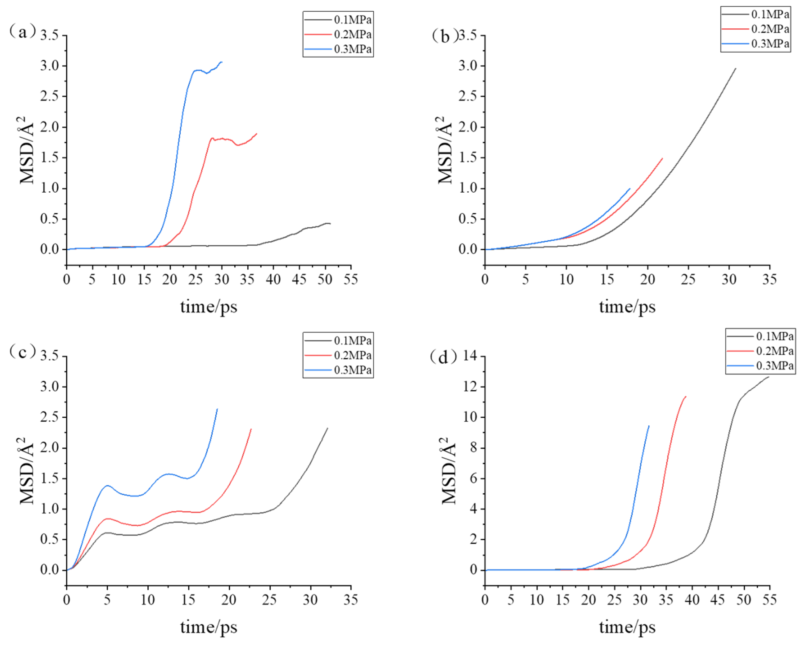
Figure 12 shows the tangential MSD changes between different material substrates and silicon wafers under applied pressure. Figure 12a–d, respectively, show the MSD changes between silicon carbide ceramics, iron–carbon alloys, aluminum–magnesium alloys, and alumina ceramics with silicon wafers. In Figure 12a,d, the MSD changes in the Newtonian layer atoms of the silicon wafers are shown, while Figure 12b,c show the changes in the Newtonian layer atoms of iron–carbon and aluminum–magnesium alloys, respectively. In Figure 12a, due to different compression distances caused by varying loads, the MSD changes differ, with larger compression distances resulting in greater tangential MSD changes. The large MSD change in Figure 12d is due to gaps between the alumina ceramics and the simulation box, allowing more atoms to move. In Figure 12b, the larger MSD at 0.1 MPa is observed because, as seen in Figure 4, iron atoms in iron–carbon alloys bond with the outermost silicon atoms during the simulation, increasing the number of iron atoms involved in bonding over time and leading to an increase in tangential MSD. The fluctuations in the curve in Figure 12c are due to significant volume changes in aluminum–magnesium alloy atoms after molecular minimization, reducing the distance between the peaks and troughs of the sinusoidal surface, causing the silicon wafer to contact the troughs and reducing the space for atomic movement, resulting in data fluctuations. Subsequently, due to the presence of adhesion forces, atoms move in the normal direction, creating more space for tangential movement and normalizing the MSD changes.
Figure 13 presents the normal MSD changes between the substrates and silicon wafers, with Figure 13a–d corresponding to the changes between silicon carbide ceramics, iron–carbon alloys, aluminum–magnesium alloys, and alumina ceramics with silicon wafers, respectively. Compared to tangential MSD changes, except for aluminum–magnesium alloys, the trends in normal MSD changes for the other groups are similar. For aluminum–magnesium alloys, the data are unaffected in the normal direction, and due to the larger MSD changes in this direction, the presence of gaps in alumina ceramics has a minimal effect on the results. Comparing alumina ceramics with silicon carbide ceramics, the results are similar, as are the results for the aluminum–magnesium alloys and iron–carbon alloys.
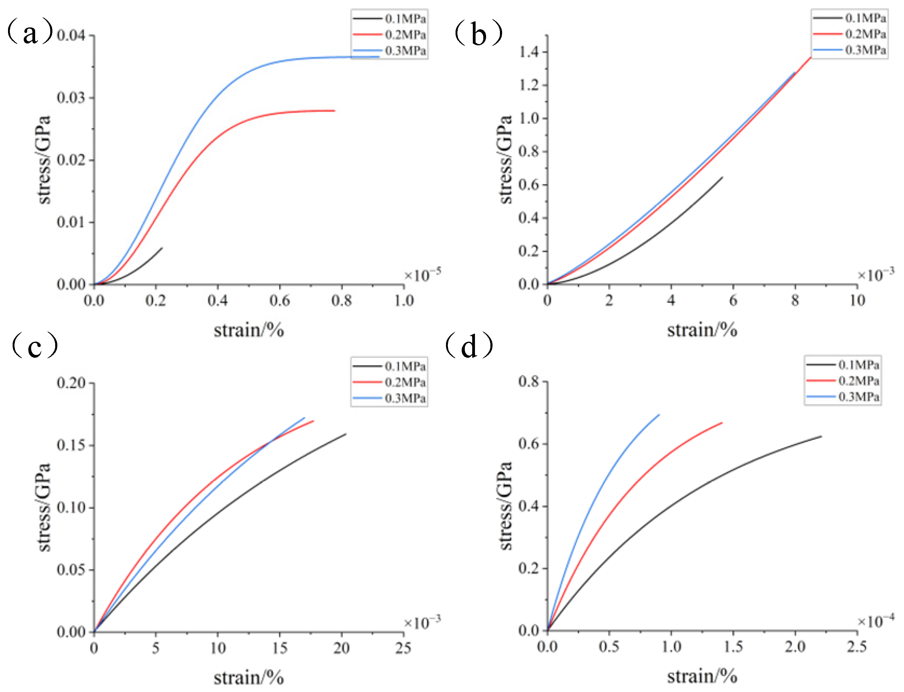
Figure 14 displays the stress–strain curves in the X direction between the substrates and silicon wafers, with Figure 14a–d representing the curves for silicon carbide ceramics, iron–carbon alloys, aluminum–magnesium alloys, and alumina ceramics with silicon wafers, respectively. Observation of the data reveals that in the iron–carbon alloy, aluminum–magnesium alloy, and alumina ceramic substrate–silicon wafer pairs, the silicon is in the elastic deformation stage during the process. When elastic deformation occurs, lower pressure and slower compression allow atoms more time to move, resulting in greater strain. Conversely, higher pressure produces greater stress for the same strain. However, in the iron–carbon alloy substrate–silicon wafer pair, due to new bonds forming between iron and silicon atoms, longer duration results in more bonded atomic pairs, reducing the resultant strain. In this process, silicon in the silicon carbide ceramic substrate–silicon wafer pair undergoes plastic deformation, with 0.1 MPa showing no plastic deformation due to shorter compression distance.
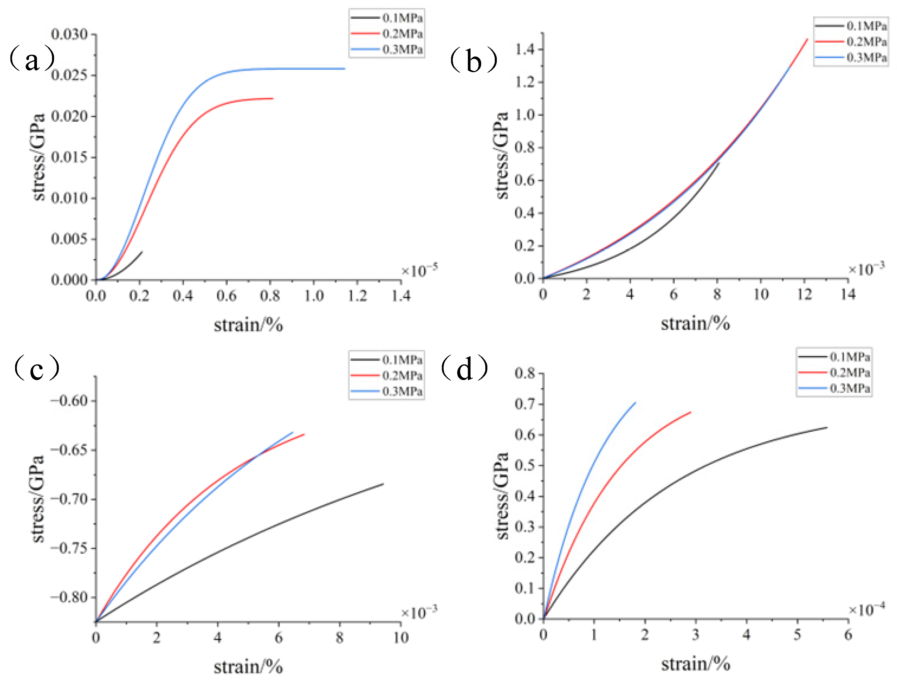
Figure 15 shows the stress–strain curves in the Y direction for the substrates and silicon wafers, with Figure 15a–d corresponding to silicon carbide ceramics, iron-carbon alloys, aluminum-magnesium alloys, and alumina ceramics with silicon wafers, respectively. Compared with the X direction, the stress values in the Y direction are lower for the same strain, which is attributed to differences in the model in the X and Y directions, though the overall trend remains consistent with the X direction.

4. Conclusions

  • Under static conditions, the tangential adhesion force of the iron–carbon alloy and aluminum–magnesium alloy was greater than that of the aluminum oxide ceramic and silicon carbide ceramic. In the normal direction, only the aluminum–magnesium alloy exhibited an attractive force when reaching a stable state.
  • During the compression simulation, the tangential adhesion force of the iron–carbon alloy was the largest, and the normal adhesion force of the aluminum–magnesium alloy was the largest.
  • During compression, the aluminum–magnesium alloy and iron–carbon alloy substrates with the silicon wafer exhibited elastic deformation. The aluminum–magnesium alloy and iron-carbon alloy underwent elastic deformation, while aluminum oxide ceramic and silicon carbide ceramic substrates with the silicon wafer showed plastic deformation when compressed with the silicon carbide ceramic and elastic deformation when compressed with the aluminum oxide ceramic.
  • These conclusions provide support for the construction of microarray structures to enhance adhesion, when the substrate is subjected to normal pressure, the deformation will increase the actual contact area, and at the same time, the tangential deformation can be increased, which will produce more actual contact area. At the same time, after unloading pressure, due to the elastic deformation of the substrate, the microgroove part of the microarray structure cannot contact the wafer, and the actual contact area is smaller than that without the microarray structure, which is more conducive to separating the wafer after processing.

Author Contributions

Conceptualization, S.H. and Z.C.; methodology, S.H. and Z.C.; software, S.H.; writing—original draft preparation, S.H., Z.Z. and Z.W.; writing—review and editing, Z.C., M.F. and Y.C. All authors have read and agreed to the published version of the manuscript.

Funding

This research was funded by the Natural Science Foundation of Zhejiang Province, China (grant No. LQ23E050003, LQ22E050008).

Data Availability Statement

The data presented in this study are available on request from the corresponding author. The data are not publicly available due to privacy.

Conflicts of Interest

The authors declare no conflicts of interest.

References

  1. Stallhofer, P. Ultra-Thin Chip Technology and Applications; Joachim Burghartz; Springer: New York, NY, USA, 2011; pp. 3–12. [Google Scholar]
  2. Zhang, Z.; Cui, J. A novel approach of mechanical chemical grinding. J. Alloys Compd. 2017, 726, 514–524. [Google Scholar] [CrossRef]
  3. Dong, Z.; Lin, Y. Ultra-thin wafer technology and applications: A review. Mater. Sci. Semicond. Process 2020, 105, 104681. [Google Scholar] [CrossRef]
  4. Zhou, L.; Eda, H. Defect-free fabrication for single crystal silicon substrate by chemo-mechanical grinding. CIRP Ann. 2006, 55, 313–316. [Google Scholar] [CrossRef]
  5. Pei, Z.J.; Strasbaugh, A. Fine grinding of silicon wafers: Designed experiments. Int. J. Mach. Tools Manuf. 2002, 42, 395–404. [Google Scholar] [CrossRef]
  6. Pei, Z.J.; Fisher, G.R. Grinding of silicon wafers: A review from historical perspectives. Int. J. Mach. Tools Manuf. 2008, 48, 1297–1307. [Google Scholar] [CrossRef]
  7. Xu, L.; Chen, H. Study on rheological properties and polishing performance of viscoelastic material for dilatancy pad. Precis. Eng. 2022, 77, 328–339. [Google Scholar] [CrossRef]
  8. Pan, B.; Kang, R. Precision fabrication of thin copper substrate by double-sided lapping and chemical mechanical polishing. J. Manuf. Process 2019, 44, 47–54. [Google Scholar] [CrossRef]
  9. Hayes, A.V.; Randive, R. Evaluation of backside particle contamination and electrostatic chuck design on the cleanliness of EUV reticle mask blanks in a multilayer Mo/Si ion beam deposition system. Proc. SPIE 2008, 7122, 1169–1184. [Google Scholar]
  10. Une, A.; Ogasawara, N. Development of a nondeforming chucking technique for EUV lithography. Microelectron. Eng. 2013, 112, 278–281. [Google Scholar] [CrossRef]
  11. Yoshitomi, K.; Une, A. Study of a clamping process with no deformation for a thin substrate using a freezing pin chuck system. Precis. Eng. 2020, 64, 45–52. [Google Scholar] [CrossRef]
  12. Yoshitomi, K.; Une, A. Study of the Warp Removal Process for a Thin Substrate: Development of a Correction Processing System Using a Freezing Pin Chuck. Int. J. Auto. Tech-Jpn. 2020, 14, 633–643. [Google Scholar] [CrossRef]
  13. Zhou, H.; Xu, X.M. In Study on improved grinding process of sapphire with LED substrate material in manufacturing engineering. Adv. Mat. Res. 2012, 583, 314–317. [Google Scholar] [CrossRef]
  14. Xu, L.; Wang, L. Effects of pH values and H2O2 concentrations on the chemical enhanced shear dilatancy polishing of tungsten. Micromachines 2022, 13, 762. [Google Scholar] [CrossRef] [PubMed]
  15. Li, Z.; Pei, Z. Machining processes for sapphire wafers: A literature review. Proc. Inst. Mech. Eng. B J. Eng. Manuf. 2011, 225, 975–989. [Google Scholar] [CrossRef]
  16. Price, G.L.; Usher, B.F. Application of epitaxial lift-off to optoelectronic material studies. In Physical Concepts of Materials for Novel Optoelectronic Device Applications I: Materials Growth and Characterization; SPIE: Bellingham, WA, USA, 1991; p. 1361. [Google Scholar]
  17. Chen, Z.; Cao, L. The mechanism of layer stacked clamping (LSC) for polishing ultra-thin sapphire wafer. Micromachines 2020, 11, 759. [Google Scholar] [CrossRef] [PubMed]
  18. Chen, Z.; Han, S. Performance assessment of ultrathin sapphire wafer polishing with layer stacked clamping (LSC) method. Int. J. Adv. Manuf. Technol. 2023, 127, 3761–3771. [Google Scholar] [CrossRef]
  19. Chen, Z.; Han, S. Analysis of the Influence of the Motion State of Ultra-Thin Sapphire Based on Layer-Stacked Clamping (LSC). Micromachines 2023, 14, 1124. [Google Scholar] [CrossRef] [PubMed]
  20. Delrio, F.W.; Carraro, C.; Maboudian, R. Small-scale surface engineering problems. In Tribology and Dynamics of Engine and Powertrain; Woodhead Publishing: Cambridge, UK, 2010; pp. 960–989. [Google Scholar]
  21. Ringl, C.; Urbassek, H.M. A LAMMPS implementation of granular mechanics: Inclusion of adhesive and microscopic friction forces. Comput. Phys. Commun. 2012, 183, 986–992. [Google Scholar] [CrossRef]
  22. Stukowski, A. Visualization and analysis of atomistic simulation data with OVITO–the Open Visualization Tool. Model. Simul. Mat. Sci. Eng. 2009, 18, 015012. [Google Scholar] [CrossRef]
  23. Tersoff, J. New empirical approach for the structure and energy of covalent systems. Phys. Rev. B 1988, 37, 6991. [Google Scholar] [CrossRef]
  24. Tersoff, J. Chemical order in amorphous silicon carbide. Phys. Rev. B 1994, 49, 16349. [Google Scholar] [CrossRef] [PubMed]
  25. Choudhary, K.; Liang, T. Charge optimized many-body (COMB) potential for Al2O3 materials, interfaces, and nanostructures. J. Phys. Condens. Matter 2015, 27, 305004. [Google Scholar] [CrossRef]
  26. Lee, B.J. A modified embedded-atom method interatomic potential for the Fe–C system. Acta Mater. 2006, 54, 701–711. [Google Scholar] [CrossRef]
  27. Mendelev, M.I.; Asta, M. Development of interatomic potentials appropriate for simulation of solid–liquid interface properties in Al–Mg alloys. Philos. Mag. 2009, 89, 3269–3285. [Google Scholar] [CrossRef]
  28. Rappé, A.K.; Casewit, C.J. UFF, a full periodic table force field for molecular mechanics and molecular dynamics simulations. J. Am. Chem. Soc. 1992, 114, 10024–10035. [Google Scholar] [CrossRef]
  29. Mayo, S.L.; Olafson, B.D. DREIDING: A generic force field for molecular simulations. J. Phys. Chem. C 1990, 94, 8897–8909. [Google Scholar] [CrossRef]
Figure 1. The simulation diagram of silicon wafers with different material substrates under static conditions. (a) The initial model of a silicon wafer–aluminum oxide ceramic substrate; (b) The initial model of a silicon wafer–iron–carbon alloy substrate; (c) The initial model of a silicon wafer–aluminum–magnesium alloy substrate; (d) The initial model of a silicon wafer–silicon carbide ceramic substrate; (e) The simulation results diagram for a silicon wafer–aluminum oxide ceramic substrate; (f) The simulation results diagram for a silicon wafer–iron–carbon alloy substrate; (g) The simulation results diagram for a silicon wafer–aluminum–magnesium alloy substrate; (h) The simulation results diagram for a silicon wafer–silicon carbide ceramic substrate.
Lubricants 12 00183 g001
Figure 2. A model when the distance between the substrate and the wafer is different. (a) The initial model of a silicon wafer–aluminum oxide ceramic substrate; (b) The initial model of a silicon wafer–iron–carbon alloy substrate; (c) The initial model of a silicon wafer–aluminum–magnesium alloy substrate; (d) The initial model of a silicon wafer–silicon carbide ceramic substrate; (e) The simulation results diagram for a silicon wafer–aluminum oxide ceramic substrate; (f) The simulation results diagram for a silicon wafer–iron–carbon alloy substrate; (g) The simulation results diagram for a silicon wafer–aluminum–magnesium alloy substrate; (h) The simulation results diagram for a silicon wafer–silicon carbide ceramic substrate.
Lubricants 12 00183 g002
Figure 3. Silicon wafer–aluminum oxide ceramic substrate. (a) Initial model; (b) Model with applied pressure of 0.1 MPa; (c) Model with applied pressure of 0.2 MPa; (d) Model with applied pressure of 0.3 MPa.
Lubricants 12 00183 g003
Figure 4. Silicon wafer–iron–carbon alloy substrate. (a) Initial model; (b) Model with applied Pressure of 0.1 MPa; (c) Model with applied pressure of 0.2 MPa; (d) Model with applied pressure of 0.3 MPa.
Lubricants 12 00183 g004
Figure 5. Silicon wafer–aluminum–magnesium alloy substrate. (a) Initial model; (b) Model with applied pressure of 0.1 MPa; (c) Model with applied pressure of 0.2 MPa; (d) Model with applied pressure of 0.3 MPa.
Lubricants 12 00183 g005
Figure 6. Silicon wafer–silicon carbide ceramic substrate. (a) Initial model; (b) Model with applied pressure of 0.1 MPa; (c) Model with applied pressure of 0.2 MPa; (d) Model with applied pressure of 0.3 MPa.
Lubricants 12 00183 g006
Figure 7. Normal adhesion between materials: (a) silicon wafer–aluminum oxide ceramic substrate; (b) silicon wafer–iron–carbon alloy substrate; (c) silicon wafer–aluminum–magnesium alloy substrate; (d) silicon wafer–silicon carbide ceramic substrate.
Lubricants 12 00183 g007
Figure 8. Tangential adhesion between materials: (a) silicon wafer–aluminum oxide ceramic substrate; (b) silicon wafer–iron–carbon alloy substrate; (c) silicon wafer–aluminum–magnesium alloy substrate; (d) silicon wafer–silicon carbide ceramic substrate.
Lubricants 12 00183 g008
Figure 9. The associated outcomes between silicon wafers and substrates under static conditions: (a) tangential adhesion force; (b) normal adhesion force; (c) MSD changes in the tangential direction; (d) MSD changes in the tangential normal direction.
Lubricants 12 00183 g009
Figure 10. Variation of tangential adhesion force between groups under different pressures: (a) silicon wafer–silicon carbide ceramic substrate; (b) silicon wafer–iron–carbon alloy substrate; (c) silicon wafer–aluminum–magnesium alloy substrate; (d) silicon wafer–aluminum oxide ceramic substrate.
Lubricants 12 00183 g010
Figure 11. Variation of normal adhesion force between groups under different pressures: (a) silicon wafer–silicon carbide ceramic substrate; (b) silicon wafer–iron–carbon alloy substrate; (c) silicon wafer–aluminum–magnesium alloy substrate; (d) silicon wafer–aluminum oxide ceramic substrate.
Lubricants 12 00183 g011
Figure 12. Variation of tangential MSD between different groups under different pressures: (a) silicon wafer–silicon carbide ceramic substrate; (b) silicon wafer–iron–carbon alloy substrate; (c) silicon wafer–aluminum–magnesium alloy substrate; (d) silicon wafer–aluminum oxide ceramic substrate.
Lubricants 12 00183 g012
Figure 13. Variation of normal MSD between different groups under different pressures: (a) silicon wafer–silicon carbide ceramic substrate; (b) silicon wafer–iron–carbon alloy substrate; (c) silicon wafer–aluminum–magnesium alloy substrate; (d) silicon wafer–aluminum oxide ceramic substrate.
Lubricants 12 00183 g013
Figure 14. Variation of strain–stress in the tangential direction between different groups under different pressures: (a) silicon wafer–silicon carbide ceramic substrate; (b) silicon wafer–iron–carbon alloy substrate; (c) silicon wafer–aluminum-magnesium alloy substrate; (d) silicon wafer–aluminum oxide ceramic substrate.
Lubricants 12 00183 g014
Figure 15. Variation of strain–stress in the normal direction between different groups under different pressures: (a) silicon wafer–aluminum oxide ceramic substrate; (b) silicon wafer–iron–carbon alloy substrate; (c) silicon wafer–aluminum–magnesium alloy substrate; (d) silicon wafer–silicon carbide ceramic substrate.
Lubricants 12 00183 g015
Table 1. Leonard–Jones force field potential constants.
Atom ε (Å) σ (kcal/mol)
Al4.4990.505
O3.5410.195
Si4.270.31
Fe4.540.055
Mg2.960.111
C3.40.0556
Disclaimer/Publisher’s Note: The statements, opinions and data contained in all publications are solely those of the individual author(s) and contributor(s) and not of MDPI and/or the editor(s). MDPI and/or the editor(s) disclaim responsibility for any injury to people or property resulting from any ideas, methods, instructions or products referred to in the content.