Article

Voltage Amplitude-Controlled Synaptic Plasticity from Complementary Resistive Switching in Alloying HfOx with AlOx-Based RRAM

Division of Electronics and Electrical Engineering, Dongguk University, Seoul 04620, Korea
*
Author to whom correspondence should be addressed.
Metals 2020, 10(11), 1410; https://doi.org/10.3390/met10111410
Submission received: 28 September 2020 / Revised: 17 October 2020 / Accepted: 22 October 2020 / Published: 23 October 2020

Abstract

:
In this work, the synaptic plasticity from complementary resistive switching in a HfAlOx-based resistive memory device was emulated by a direct current (DC) voltage sweep, current sweep, and pulse transient. The alloyed HfAlOx dielectric was confirmed by X-ray photoelectron spectroscopy analysis. The negative differential resistance observed before the forming and set processes can be used for interface resistive switching with a low current level. Complementary resistive switching is obtained after the forming process at a negative bias. This unique resistive switching is also suitable for synaptic device applications in which the reset process occurs after an additional set process. The current sweep mode provides more clear information on the complementary resistive switching. Multiple current states are achieved by controlling the amplitude of the set and reset voltages under DC sweep mode. The potentiation and depression characteristics are mimicked by varying the pulse voltage amplitude for synaptic device application in a neuromorphic system. Finally, we demonstrate spike-timing-dependent plasticity by tuning the timing differences between pre-spikes and post-spikes.

1. Introduction

The von Neumann bottleneck makes the memory access time delayed because of the separation of the computing part and memory part in modern complementary metal-oxide-semiconductor (CMOS) computing systems. In the era of big data, more energy efficient and faster computing systems are needed to overcome the limitations of von Neumann architecture. In-memory computing processing is the next promising technology, which, unlike conventional computing, loads and uses all the data into memory [1]. Moreover, brain-inspired computing systems emulating synapses and neurons are proposed for the pursuit of better computing systems [2]. In the neuromorphic chip, a single semiconductor chip performs storage and computation with low energy consumption, and it has specializations for complex tasks such as pattern and speech recognition analysis [3]. The memristor is versatile electron memory element that is applicable to synaptic devices [4,5,6] as well as high-density memory applications [7,8,9,10,11,12]. Among several categories, oxide-based resistive random-access memory (RRAM) is very promising due to its stable and reliable resistive-switching properties such as good variability, long program/erase cycle endurance, long data retention, and complementary metal-oxide-semiconductor (CMOS) compatibility [13]. To date, various resistive switching characteristics of a lot of metal oxides such as ZrOx, TaOx, AlOx, ZnOx, and TiOx have been reported [14,15,16,17,18]. Among them, HfOx is one of the most popular resistive-switching materials due to its outstanding resistive-switching characteristics [18]. The HfO2 dielectric is commonly used in dynamic random-access memory (DRAM) capacitors and gate insulators in metal-oxide-semiconductor field-effect transistors. Excellent resistive-switching behaviors from the movement of oxygen vacancies in the HfO2 dielectric are also achieved [18].
The resistive switching of metal-oxide-based RRAM is classified under three main categories. The first one is electrochemical metallization (ECM), in which the metallic filament is created from the top electrode with high diffusion ability such as Ag and Cu [19]. Metal oxides can be a medium material for metallic filaments from the electrode. The second one is the valence change mechanism (VCM) in which the oxygen vacancies’ movements are the main reason for the resistive switching [18]. The metal-oxide-based RRAM using a VCM has shown the best resistive-switching performance to date [17]. The last one is the thermal–chemical mechanism (TCM), in which unipolar switching occurs with Joule heating. However, TCM-based switching’s performance parameters such as endurance, variability, and reproducibility are not good for commercialization. Al2O3 incorporation in a HfO2 dielectric can enhance the resistive-switching characteristics according to several reports [20,21]. Complementary resistive switching (CRS) has the advantage of nonlinear I–V characteristics, which include selector function. Thus, it increases the read margin by reducing sneak current in the crossbar array structure [13]. We reported nonlinear CRS characteristics in a single-layer HfAlOx dielectric in our past report [21].
Here, the voltage-controlled synaptic behaviors and current sweep mode are proposed in a Pt/Al-incorporated HfOx/TiN device for neuromorphic applications. Firstly, the alloy-type HfAlOx dielectric was investigated by X-ray photoelectron spectroscopy (XPS) analysis. The CRS behavior and negative differential resistance were closely studied by the current sweep method as well as the voltage sweep method. The current sweep can provide more delicate information hidden by the compliance current in a negative bias region for CRS. Interface-type bipolar switching is made available by selecting a negative differential resistance (NDR) for the reset process. In the CRS, multiple levels are obtained by the fine adjustment of the voltage amplitude for a desirable synaptic device. The potentiation and depression characteristics are imitated by pulse events for neuromorphic applications. Furthermore, spike-timing-dependent plasticity (STDP) behavior is emulated by controlling the timing overlapping of two input pulses with different pulse amplitudes.

2. Materials and Methods

The Pt/HfAlOx/TiN device was fabricated as follows: A 100 nm-thick TiN layer was deposited on a SiO2/Si wafer using direct current (DC) sputtering. Some 7 nm-thick HfAlOx were deposited with an atomic layer deposition (ALD) system (NCD, Daejeon, Korea). Tetrakis (ethylmethylamino) hafnium (TEMAH) and trimethylaluminum (TMA) were used as the metal precursors for a HfO2 film and Al2O3 film, respectively. H2O was used as the oxidant for both layers. One cycle of (TMA + H2O) and 11 cycles of (TEMAH + H2O) deposition were alternatively performed a total of 8 times to incorporate the Al in the HfO2 dielectric (Figure 1). The substrate temperature was 280 °C for the HfAlOx deposition. A 100 nm-thick Pt top electrode was deposited with an e-beam evaporator system and patterned by a shadow mask containing circular patterns with a diameter of 100 μm. The electrical properties were characterized in DC mode using a Keithley 4200-SCS semiconductor parameter analyzer (Keithley, Solon, OH, USA) and in pulse mode using a 4225-PMU ultrafast module (Keithley, Solon, OH, USA). During the measurements, a bias voltage and pulse were applied to the Pt top electrode, while the TiN bottom electrode was grounded.

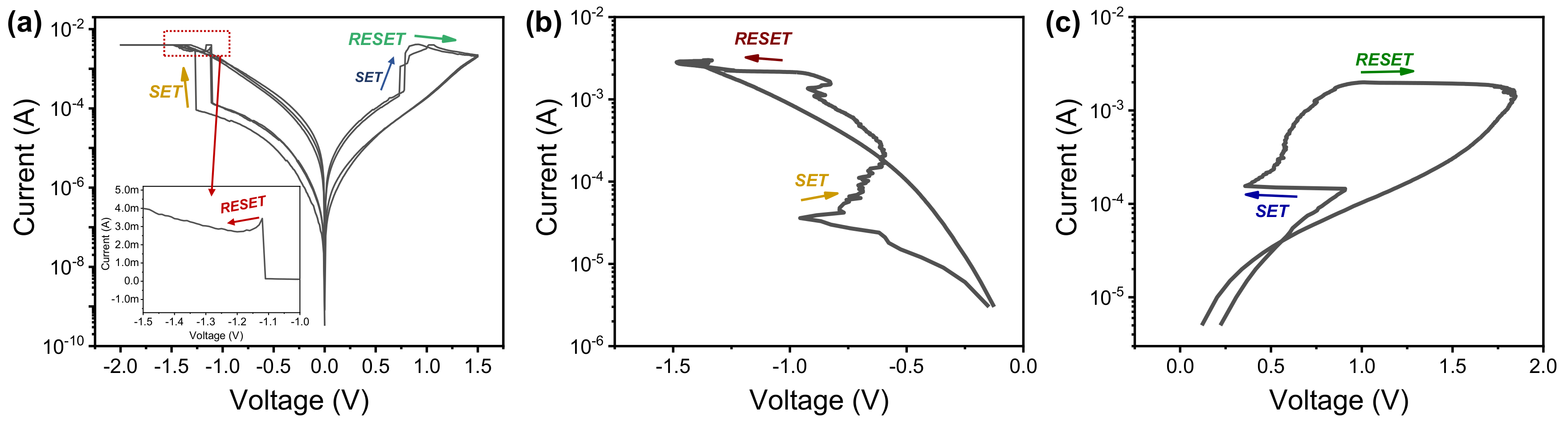
3. Results and Discussion

Figure 2 shows the XPS spectra of the HfAlOx alloy film. Figure S1 shows the survey scan of the HfAlOx film. The binding energy peaks are centered at about 18.3 and 19.5 eV, corresponding to Hf4f7/2 and Hf4f5/2 core-level electrons, respectively (Figure 2a) [22,23]. Two peaks are slightly higher than the values in previous reports. As the Al content increases in a HfAlOx film, the peak of the binding energy tends to increase [24]. Figure 2b shows the Al 2p spectra of the HfAlOx dielectric. Al 2p spectra have higher noise because the number of Al2O3 cycles is much lower compared to the HfO2 cycles during ALD deposition [20]. However, the peak of the binding energy (~75 eV) is clearly observed for Al 2p (Figure 2b) [20]. A similar result is reported for the Al-doped HfO2 film. The binding energy peak is located at 531.7 eV, which corresponds to O1s [23]. This peak value is also higher than that for pure HfO2 film due to the Al incorporation in the HfO2 film. Additionally, we characterized the HfAlOx film on indium tin oxide (ITO) glass with different x values and revealed the x value’s effect on the resistive switching in our previous work [12]. Basically, when the Al content increases, the energy band gap of the HfAlOx layer increases and the insulating property increases [12].
The initial current–voltage (IV) characteristics were investigated by DC voltage and current sweep methods (Figure 3a,b). Forming in negative bias is preferred for resistive switching because the TiN bottom electrode is more suitable for the oxygen exchange layer than the Pt top electrode [25,26].
The IV curves with a relatively large variation include the NDR before the forming process (abrupt current jump) in Figure 3a [27]. The initial reset was selected for a formation-less process when the NDR region was used. We will discuss the bipolar resistive switching later when using an NDR in the first switching. The reset process is observed in the NDR region with the current sweep mode (Figure 3b). Moreover, multiple set transitions are markedly observed before the abrupt SET process in the current sweep method. The temporal transition is related to the defect distribution of the dielectric [28]. Next, the reset process occurs after the set process in a positive bias and a negative bias, as shown in Figure 4. The CRS curves are more distinctively observed in a positive bias region compared to the negative bias region. The reset process is not clearly observed (inset of Figure 4a) after the abrupt set process in the voltage sweep method in a negative bias region because the reset process is hidden by the compliance of 3 mA (Figure 4a). Here, compliance is used to prevent the permanent breakdown of the device. The current in a backward sweep is clearly higher than that in a forward sweep, indicating that the set process is the more dominant process under the negative bias in dual sweep mode. On the other hand, the reset process is the more dominant process than the set process in a positive bias. We presented a possible conducting filament-based switching model in the past [21]. The CRS behavior can be more clearly observed in the current sweep mode. The resistance reduction in the snap-back region means the set process occurs in the current sweep mode of the negative voltage region (Figure 4b). The voltage amplitude is increased at over 1 mA for the reset process (Figure 4b). The current in a backward sweep is significantly increased compared to the that in a forward sweep at the read voltage of −0.5 V. The set and reset processes in a positive voltage region are observed in a similar way as in the negative voltage region, but the current is notably decreased at a backward sweep compared to that at a forward sweep (Figure 4c). The bipolar resistive-switching (BRS) characteristic is obtained by using the reset process in the NDR region of the Pt/HfAlOx/TiN device. The conversion from CRS to BRS is shown in Figure S1. An additional RESET process (second sweep) occurs in a negative bias after the reset (first sweep) in a positive bias. Subsequently, the repeatable set process and reset process are observed in the positive bias and negative bias in Figure S1, respectively.
Next, the multiple levels are demonstrated by controlling the voltage amplitude under the DC sweep mode for CRS before emulating the synapse functions. We focus on the multi-level properties in the positive bias because CRS is more clearly observed in the positive bias. The non-volatile property is confirmed by stopping the peak current at the set process in red color (Figure 5a). The IV at the forward sweep (blue color) for the reset process is nearly same as the IV at the backward sweep for the set process. The voltage range of the conductance transition region in the set process is smaller than that in the reset process. Thus, we can control the smaller reset voltage, so more sophisticated voltage control is required. The current tends to increase gradually with the DC voltage sweep from 0.6 to 0.92 V, with an incremental voltage of 0.02 V (Figure 5b). Conversely, a multiple reset process is achieved by controlling the reset stop voltage from 0.94 to 1.51 V, with an incremental voltage of 0.1 V (Figure 5c). The results indicate that the multi-level cells (MLC) can be implemented by just the voltage amplitude in the positive bias of CRS.
To further demonstrate the MLC for neuromorphic applications, the current response was monitored by pulse inputs. Fifty pairs were applied as the read voltage of 0.5 V and the set voltage of 0.9 V alternated for potentiation. Then, immediately, 50 pairs (read voltage: 0.5 V and reset voltage: 1.05 V) were applied for depression (Figure 6). The current gradually increased in 50 set pulses and then gradually decreased in the reset pulse. It is to be noted that the well-controlled potentiation/depression is only implemented by the voltage amplitude. The inset of Figure 6 shows the gradually controlled conductance that is conversion from the current at 0.2 V for potentiation and depression. STDP is a key biological learning process that controls the synaptic weight between neurons. The strengths of connections in a biological synapse are adjusted by the relative timing differences between pre-spikes and post-spikes from neurons. The fact that the bio-inspired synaptic device mimics the actual biological working method of neurons and synapses such as STDP indicates that it comes a step closer to a neuromorphic system. To emulate the STDP in biological synapses, we firstly designed the scheme of the pre- and post-spike train (Figure 7). The pre-spike consists of a single pulse, and the post-spike consists of several pulses with different voltage amplitudes, as shown in Figure 7b. The single pulse pre-spike overlaps the pulse with a smaller amplitude when the pre-spike leads the post-spike (Figure 7a). The main pulse with highest voltage amplitude should be the range of the set voltage for potentiation. On the other hand, the single pulse in the pre-spike is overlapped in the highest pulse that is in the range of the reset voltage for depression when the pre-spike lags the post-spike (Figure 7c). The current responses by the overlapped pulse trains of the pre-spike and post-spike are obtained for potentiation and depression as shown in Figure 8a,b, respectively. When the pre-spike precedes the post-spike by 200 μs, the fourth one of the pulse train is an effective pulse that causes a current change (Figure 8a). The current is gradually increased when the fourth pulse is applied, which is well matched with the above measurement results. When the pre-spike is behind the post-spike by 200 μs, the sixth pulse of the pulse train is an effective pulse that causes a reset process for depression (Figure 8b). The current gradually decreases when the sixth pulse is applied. Finally, we obtain the STDP curves by scanning a wider range of timing differences (Figure 8c). The synaptic weight change increases as the spike timing difference increases.

4. Conclusions

In summary, voltage-controlled STDP was demonstrated in a Pt/HfAlOx/TiN memristor device. The alloying-type HfAlOx film was verified by XPS analysis. The unique CRS characteristics in Pt/HfAlOx/TiN were extensively investigated by both DC voltage and current sweep modes. The NDR and the hidden resistive switching by current compliance are more clearly observed in DC sweep mode. The NDR provides another switching mode for the homogeneous type. The CRS in the Pt/HfAlOx/TiN device is applicable to the synaptic application. The gradual set process and reset process occur at low voltage and high voltage regions, respectively, which are controllable for MLC by incremental voltage amplitude changes. For more practical operation, the potentiation and depression can be achieved by voltage amplitude-controlled pulses. Finally, we emulated the STDP of the biological synapse by designing a pulse train scheme for pre-spikes and post-spikes.

Supplementary Materials

The following are available online at https://www.mdpi.com/2075-4701/10/11/1410/s1. Figure S1: XPS survey scan of HfAlOx film. Figure S2: Transient characteristics of complementary resistive switching to bipolar resistive switching (interface).

Author Contributions

H.R. and J.C. conducted the electrical measurements and wrote the manuscript. S.K. designed the experiment concept and supervised the study. All authors have read and agreed to the published version of the manuscript.

Funding

This work was supported in part by the National Research Foundation of Korea (NRF), a grant funded by the Korean government (MSIP) under Grant 2018R1C1B5046454.

Conflicts of Interest

The authors declare no conflict interest.

References

  1. Graves, C.E.; Li, C.; Sheng, X.; Miller, D.; Ignowski, J.; Kiyama, L.; Strachan, J.P. Nater. In-Memory Computing with Memristor Content Addressable Memories for Pattern Matching. Adv. Mater. 2020, 32, 2003437. [Google Scholar] [CrossRef] [PubMed]
  2. Xia, Q.; Yang, J.J. Memristive crossbar arrays for brain-inspired computing. Nater. Mater. 2019, 18, 309–323. [Google Scholar] [CrossRef] [PubMed]
  3. Ryu, H.; Kim, S. Pseudo-Interface Switching of a Two-Terminal TaOx/HfO2 Synaptic Device for Neuromorphic Applications. Nanomaterials 2020, 10, 1550. [Google Scholar] [CrossRef] [PubMed]
  4. Mikhaylov, A.; Pimashkin, A.; Pigareva, Y.; Gerasimova, S.; Gryaznov, E.; Shchanikov, S.; Zuev, A.; Talanov, M.; Lavrov, I.; Demin, V.; et al. Neurohybrid Memristive CMOS-Integrated Systems for Biosensors and Neuroprosthetics. Front. Mol. Neurosci. 2020, 14, 358. [Google Scholar] [CrossRef]
  5. Emelyanov, A.V.; Nikiruy, K.E.; Serenko, A.V.; Sitnikov, A.V.; Presnyakov, M.Y.; Rybka, R.B.; Sboev, A.G.; Rylkov, V.V.; Kashkarov, P.K.; Kovalchuk, M.V.; et al. Self-adaptive STDP-based learning of a spiking neuron with nanocomposite memristive weights. Nanotechnology 2020, 31, 045201. [Google Scholar] [CrossRef]
  6. Cho, S.; Kim, S. Emulation of Biological Synapse Characteristics from Cu/AlN/TiN Conductive Bridge Random Access Memory. Nanomaterials 2020, 10, 1709. [Google Scholar] [CrossRef]
  7. Kim, S.; Jung, S.; Kim, M.-H.; Chen, Y.-C.; Chang, T.-C.; Ryoo, K.-C.; Cho, S.; Lee, J.-H.; Park, B.-G. Scaling Effect on Silicon Nitride Memristor with Highly Doped Si Substrate. Small 2018, 14, 1704062. [Google Scholar] [CrossRef]
  8. Mikhaylov, A.; Belov, A.; Korolev, D.; Antonov, I.; Kotomina, V.; Kotina, A.; Gryaznov, E.; Sharapov, A.; Koryazhkina, M.; Kryukov, R.; et al. Multilayer Metal-Oxide Memristive Device with Stabilized Resistive Switching. Adv. Mater. Technol. 2020, 5, 1900607. [Google Scholar] [CrossRef]
  9. Ryu, J.-H.; Kim, S. Improved Intrinsic Nonlinear Characteristics of Ta2O5/Al2O3-Based Resistive Random-Access Memory for High-Density Memory Applications. Materials 2020, 13, 4201. [Google Scholar] [CrossRef]
  10. Maikap, S.; Banergee, W. In Quest of Nonfilamentary Switching: A Synergistic Approach of Dual Nanostructure Engineering to Improve the Variability and Reliability of Resistive Random-Access-Memory Devices. Adv. Electron. Mater. 2020, 6, 2000209. [Google Scholar] [CrossRef]
  11. Kim, S.; Park, B.G. Nonlinear and multilevel resistive switching memory in Ni/Si3N4/Al2O3/TiN structures. Appl. Phys. Lett. 2016, 108, 212103. [Google Scholar] [CrossRef]
  12. Mahata, C.; Kim, S. Modified resistive switching performance by increasing Al concentration in HfO2 on transparent indium tin oxide electrode. Ceram. Int. 2020. [Google Scholar] [CrossRef]
  13. Linn, E.; Rosezin, R.; Kügeler, C.; Waser, R. Complementary resistive switches for passive nanocrossbar memories. Nat. Mater. 2010, 9, 403–406. [Google Scholar] [CrossRef] [PubMed]
  14. Lanza, M.; Wong, H.-S.P.; Pop, E.; Ielmini, D.; Strukov, D.; Regan, B.C.; Larcher, L.; Villena, M.A.; Yang, J.J.; Goux, L.; et al. Recommended Methods to Study Resistive Switching Devices. Adv. Electron. Mater. 2018, 5, 1800143. [Google Scholar] [CrossRef] [Green Version]
  15. Salaoru, I.; Prodromakis, T.; Khiat, A.; Toumazou, C. Resistive switching of oxygen enhanced TiO2 thin-fim devices. Appl. Phys. Lett. 2013, 102, 013506. [Google Scholar] [CrossRef]
  16. Yang, Y.; Sheridan, P.; Lu, W. Complementary resistive switching in tantalum oxide-based resistive memory devices. Appl. Phys. Lett. 2012, 100, 203112. [Google Scholar] [CrossRef]
  17. Lee, M.-J.; Lee, C.B.; Lee, D.; Lee, S.R.; Chang, M.; Hur, J.H.; Kim, Y.-B.; Kim, C.-J.; Seo, D.H.; Seo, S.; et al. A fast, high-endurance and scalable non-volatile memory device made from asymmetric Ta2O5−x/TaO2−x bilayer structures. Nat. Mater. 2011, 10, 625–630. [Google Scholar] [CrossRef]
  18. Chen, X.; Hu, W.; Li, Y.; Wu, S.; Bao, D. Complementary resistive switching behaviors evolved from bipolar TiN/HfO2/Pt device. Appl. Phys. Lett. 2016, 108, 053504. [Google Scholar] [CrossRef]
  19. Bricalli, A.; Ambrosi, E.; Laudato, M.; Maestro, M.; Rodriguez, R.; Ielmini, D. Resistive Switching Device Technology Based on Silicon Oxide for Improved ON–OFF Ratio—Part II: Select Devices. IEEE Trans. Electron Devices 2017, 65, 122–128. [Google Scholar] [CrossRef] [Green Version]
  20. Wu, L.; Liu, H.; Li, J.; Wang, S.; Wang, X. A Multi-level Memristor Based on Al-Doped HfO2 Thin Film. Nanoscale Res. Lett. 2019, 14, 177. [Google Scholar] [CrossRef] [PubMed] [Green Version]
  21. Choi, J.; Kim, S. Nonlinear Characteristics of Complementary Resistive Switching in HfAlOx-Based Memristor for High-Density Cross-Point Array Structure. Coatings 2020, 10, 765. [Google Scholar] [CrossRef]
  22. Zhang, L.; Liu, M.; Ren, W.; Zhou, Z.; Dong, G.; Zhang, Y.; Peng, B.; Hao, X.; Wang, C.; Jiang, Z.D.; et al. ALD preparation of high-k HfO2 thin films with enhanced energy density and efficient electrostatic energy storage. RSC Adv. 2017, 7, 8388. [Google Scholar] [CrossRef] [Green Version]
  23. Wang, L.G.; Qian, X.; Cao, Y.Q.; Cao, Z.Y.; Fang, G.Y.; Li, A.D.; Wu, D. Excellent resistive switching properties of atomic layer-deposited Al2O3/HfO2/Al2O3 trilayer structures for non-volatile memory applications. Nanoscale Res. Lett. 2015, 10, 135. [Google Scholar] [CrossRef] [PubMed] [Green Version]
  24. Ma, F.; Sun, J.; Zhang, G.; Liang, G.; Xin, Q.; Li, Y.; Song, A. Lowetemperature fabrication of HfAlO alloy dielectric usingatomicelayer deposition and its application in a lowepower device. J. Alloys Compd. 2019, 792, 543–549. [Google Scholar] [CrossRef]
  25. Jeon, H.; Park, J.; Jang, W.; Kim, H.; Kang, C.; Song, H.; Kim, H.; Seo, H.; Jeon, H. Stabilized resistive switching behaviors of a Pt/TaOx/TiN RRAM under different oxygen contents. Phys. Status Solidi (a) 2014, 9, 2189–2194. [Google Scholar] [CrossRef]
  26. Liu, Y.; Ouyang, S.; Yang, J.; Tang, M.; Wang, W.; Li, G.; Zou, Z.; Liang, Y.; Li, Y.; Xiao, Y.; et al. Effect of film thickness and temperature on the resistive switching characteristics of the Pt/HfO2/Al2O3/TiN structure. Solid State Electron. 2020, 173, 107880. [Google Scholar] [CrossRef]
  27. Ismail, M.; Kim, S. Negative differential resistance effect and dual resistive switching properties in a transparent Ce-based devices with opposite forming polarity. Appl. Surf. Sci. 2020, 530, 147284. [Google Scholar] [CrossRef]
  28. Zhou, F.; Chang, Y.F.; Fowler, B.; Byun, K.; Lee, J.C. Stabilization of multiple resistance levels by current-sweep in SiOx-based resistive switching memory. Appl. Phys. Lett. 2015, 106, 063508. [Google Scholar] [CrossRef] [Green Version]
Figure 1. Device configuration of Pt/HfAlOx/Si device.
Metals 10 01410 g001
Figure 2. X-ray photoelectron spectroscopy (XPS) spectra of HfAlOx dielectric. (a) Hf 4f; (b) Al 2p; (c) O1s.
Metals 10 01410 g002
Figure 3. Forming I–V characteristics: (a) DC voltage sweep method; (b) DC current sweep method.
Metals 10 01410 g003
Figure 4. I–V characteristics for set and reset characteristics: (a) DC voltage sweep method; (b) set process and (c) reset process in DC current sweep method.
Metals 10 01410 g004
Figure 5. (a) DC dual voltage sweep range for complementary resistive switching (CRS) in a positive bias; multi-level process by DC sweep for (b) set and (c) reset.
Metals 10 01410 g005
Figure 6. Potentiation and depression characteristics in current response from repeating set and reset pulses (pulse width: 100 μs).
Metals 10 01410 g006
Figure 7. Pulse train scheme for spike-timing-dependent plasticity (STDP). (a) Potentiation case: pre-spike leads post-spike; (b) the pre- and post-spikes at zero interval time; (c) depression case: pre-spike lags post-spike.
Metals 10 01410 g007
Figure 8. Current response with overlapped pulse train for (a) potentiation and (b) depression; (c) synaptic weight change as a function of spike timing interval for STDP characteristics.
Metals 10 01410 g008
Publisher’s Note: MDPI stays neutral with regard to jurisdictional claims in published maps and institutional affiliations.

