Review

A Bibliometric Analysis of the Publications on In Doped ZnO to be a Guide for Future Studies

1
Department of Science Teaching, K. K. Education Faculty, Atatürk University, 25240 Erzurum, Turkey
2
Advanced Materials Research Laboratory, Department of Nano science and Nano engineering, Graduate School of Natural and Applied Sciences, Ataturk University, 25240 Erzurum, Turkey
3
ENEA-Italian National Agency for New Technologies, Energy and Sustainable Economic Development, Energy Technologies Department, Casaccia Research Centre, Via Anguillarese 301, 00123 Roma, Italy
4
Department of Basic Sciences, Science Faculty, Erzurum Technical University, 25240 Erzurum, Turkey
5
Photonic Group, High Technology Research Centre (YUTAM), Erzurum Technical University, 25240 Erzurum, Turkey
*
Author to whom correspondence should be addressed.
Metals 2020, 10(5), 598; https://doi.org/10.3390/met10050598
Submission received: 7 April 2020 / Revised: 28 April 2020 / Accepted: 29 April 2020 / Published: 4 May 2020
(This article belongs to the Special Issue Metal Oxides)

Abstract

:
This study aims to examine the studies regarding In doped ZnO published in the Web of Science database. A total of 777 articles were reached (31 March 2020). The articles were downloaded for the bibliometric analysis and collected in a file. The file was uploaded to VOSViewer programme in order to reveal the most used keywords, words in the abstracts, citation analyses, co-citation and co-authorship and countries analyses of the articles. The results showed that the most used keywords were “ZnO”, “photoluminescence”, “optical properties”, “thin films” and “doping”. These results indicate that the articles mostly focus on some characteristics of In doped ZnO thin films such as structural, optical and electrical features. When the distribution of the number of articles using the keywords by year was searched, it was found that recent articles focus mainly on synthesis of In doped ZnO film via chemical routes such as sol-gel and hydrothermal syntheses, and on ZnO-based device applications such as solar cells and gas sensors. The most used keywords were also found to be films, X-ray, glass substrate, X-ray Diffraction (XRD), spectra and layer. These results indicate that the studies mostly focus on In doped ZnO thin films as transparent conductive oxide (TCO) material used in device applications like solar cells. In this context, it was found that structural, topographical, optical, electrical and magnetic properties of In doped ZnO films were characterized in terms of defected structure or defect type, substrate temperature, film thickness and In doping content. When the distribution of these words is shown on a year-by-year basis, it is evident that more recent articles tend to focus both on efficiency and performance of In doped ZnO films as TCO in solar cells, diodes and photoluminescence applications both on nanostructures, such as nanoparticles, and nanorods for gas sensor applications. The results also indicated that Maldonado and Asomoza were the most cited authors in this field. In addition, Major, Minami and Ozgur were the most cited (co-citation) authors in this field. The most cited journals were found to be Thin Solid Films, Journal of Materials Science Materials in Electronics and Journal of Applied Physics and, more recently, Energy, Ceramics International, Applied Physics-A, Optik, Material Research Express, ACS Applied Materials and Interfaces and Optical Materials. The most co-cited journals were Applied Physics Letters, Thin Solid Films, Journal of Applied Physics, Physical Review B, and Applied Surface Science. Lastly, the countries with the highest number of documents were China, India, South Korea, USA and Japan. Consequently, it is suggested that future research needs to focus more on synthesis and characterization with different growth techniques which make In doped ZnO suitable for device applications, such as solar cells and diodes. In this context, this study may provide valuable information to researchers for future studies on the topic.

1. Introduction

Indium, whose abundance in earth is similar to silver, is one of the rare metals in the earth’s crust and is nearly found as a trace element in other minerals. The importance of indium metal and its salts in organic synthesis has been recognized due to the unusual carbon–carbon bond promotion discovered in recent years, its rearrangement reactions and its performance in various beneficial reactions [1,2]. Indium is a metal with a silver-white color and a low melting point, belonging to the metal group, and it does not have the electronic structure of inert gases when it loses its outermost orbital electrons. Therefore, indium is not reactive like typical metals. Compared with lead, it is softer and malleable, but does not oxidize depending on the temperature [3,4]. Indium has also a very special functional application because it is frequently used in semiconductor based devices, thermistors and optical devices. This not only increases the popularity of indium, but also increases the need for indium in these applications. In other words, due to the demand of companies operating in the solar and wind sectors, as Hoffman et al. [5] mentioned in their studies, the demand for indium in addition to tellurium, gallium, dysprosium and neodymium is expected to increase significantly in the coming years. Considering the increasing energy need with the development of technology, it can be concluded that an element that has the status of rare elements in the earth’s crust, like indium, should be used carefully. Moreover, indium has been listed recently as a critical raw material (CRM) by the European Union, due to its high supply risk and its high economic importance [6]. Indium is mainly used as indium tin oxide (ITO), which is the transparent conductive oxide of choice in a wide range of applications, from solar cells to LED panels. ITO’s main constituent is indium (ITO contains approximately 78% indium), and therefore, researchers have focused recently on searching for ITO-alternative materials for optoelectronic applications. Among the proposed alternatives, zinc oxide steps forwards due to its unique properties such as its wide and direct band gap (≈3.3 eV), large exciton binding energy (60 meV), highly transparency in visible range and low cost [7,8,9]. Additionally, easy tunability of its morphology for the application type makes it a very suitable material for solar cells, energy hydrogen conversion devices and sensors [10,11]. From studies on ZnO films, it can be seen that pure ZnO thin films are not very stable during chemisorption and desorption of oxygen due to variable surface conductance [12]. An efficient way to reduce this disadvantage is doping [13]. The properties of ZnO can be controlled by doping and thus tailored for the desired applications. For example, although ZnO has natural n-type electrical conductivity associated with zinc interstitial and oxygen deficiency, ZnO with p-type electrical conductivity can be obtained by doping with La and As [14]. In reality, the growth of stable ZnO films with p-type conductivity is very difficult. Therefore, it is important to determine suitable dopant materials before the experimental procedure. Feng and Xia [15] found that although a large amount of dopants such as N, P, Sb, Co may be used to obtain ZnO with p-type doping, it is difficult to obtain ZnO with stable p-type conductivity due to their low solubility and deep level of acceptor characteristics. However, with the addition of arsenic to ZnO, a complex acceptor (AsZn-2Vzn) with relatively high ionization energy (137 meV) is formed. Thus, ZnO with stable p-type conductivity is obtained. Al, B, In, Ga are generally used to obtain n-type degenerate electrical semiconductors [16], due to the increase of free electrons concentration. Therefore, ZnO may be doped with several elements to achieve both n- and p-type conductivity. In order to reveal the general research tendency in the study of ZnO, a bibliometric mapping analysis was performed. Bibliometrics is an emerging cross-disciplinary analysis based on statistic and mathematic tools to map the state of the art and the development in a given area of scientific knowledge [17,18,19,20]. It allows us to identify essential information on a particular topic based on the analysis of citations, co-citations, geographical distribution and word frequency, etc., revealing the current research situation and giving insight into the future trends. In our study, the bibliometrics analysis (5439 articles were reached with keywords of ("dop*") AND (ZnO OR "zinc oxide")) was obtained by analyzing the articles published in the last three years on doped ZnO and examining them in terms of the distribution of the most frequently mentioned words in the abstracts. The results are reported in Figure 1.
From Figure 1, it can be observed that the frequency of the words “film”, “performance”, “device”, “electrode”, “power conversion efficiency”, “sensor”, “degradation” is high. This means that ZnO has a very wide range of applications. Nevertheless, the bibliometric analysis evidenced high interest towards Al doped ZnO (AZO), which is the most investigated ITO alternative, and In was selected in this review as the ZnO dopant, because it has the advantage of less reactivity and higher oxidation resistance than other additives of the same group [21]. Indium is, at present, listed among CRMs, however its content in indium doped zinc oxide (IZO) is quite low with respect to ITO. It is well known that the characteristics of ZnO depend both on the dopant content as well as on the growth condition and the growth technique. In some studies, [22,23] the dopant was limited in the range of 4 at.%–5 at.% because at a further doping ratio, the deterioration of the ZnO crystal structure or higher resistivity were found. Moreover, the electronegativity of foreign ions and standard electrode potentials (SEP) also affect carrier suppression abilities [24]. In this context, considering the electronegativity (1.78), standard electrode potential (−0.25 V) and ionic radius of indium (0.08 nm for In3+), In can be considered as a suitable dopant for ZnO in applications requiring high conductivity and optical transmission [25,26]. Therefore, in applications which require the use of indium doped tin oxide, the use of indium doped ZnO films with same optoelectronic properties can strongly reduce the use of indium. Shaheera et al. [27] grew In doped ZnO via the radio frequency (RF) sputtering technique and showed that the samples analyzed in their study can be used in white light source and LED device applications. In another study, Yu et al. [28] obtained oxygen defect rich In doped ZnO nanostructures by using a facile solution method followed by an annealing process, and proved that the photocatalytic features of ZnO improved as a result of In3+ addition into the ZnO. Bhatia and Verma [29] also investigated the performance of In doped ZnO films obtained by the rapid sol-gel dip coating technique in gas sensing application and showed that In doped ZnO films are good candidates for NO2 gas sensing due to their quick response time of 65 s and a fast recovery time of 87 s. Kyaw et al. [30] used sol-gel coated indium doped ZnO films and investigated film performance in organic solar cell applications. They obtained films with 5.54 × 10⁻¹ Ωcm−1 resistivity and 80% optical transparency which exhibited good performance as buffer layers in organic solar cell applications. In summary, as can be concluded from the aforementioned discussion, In doped ZnO has been widely used for different applications. Therefore, it is important to examine literature in detail for future studies. In our work, the studies regarding indium doped ZnO published to date in the Web of Science database were analyzed by the bibliometric analysis method. Some insights into the characteristics of IZO films are given and discussed on the basis of data from literature. Therefore, since the current study covers important studies about this subject and includes basic discussions, it will help researchers by providing a detailed background to guide their work.

2. Materials and Methods
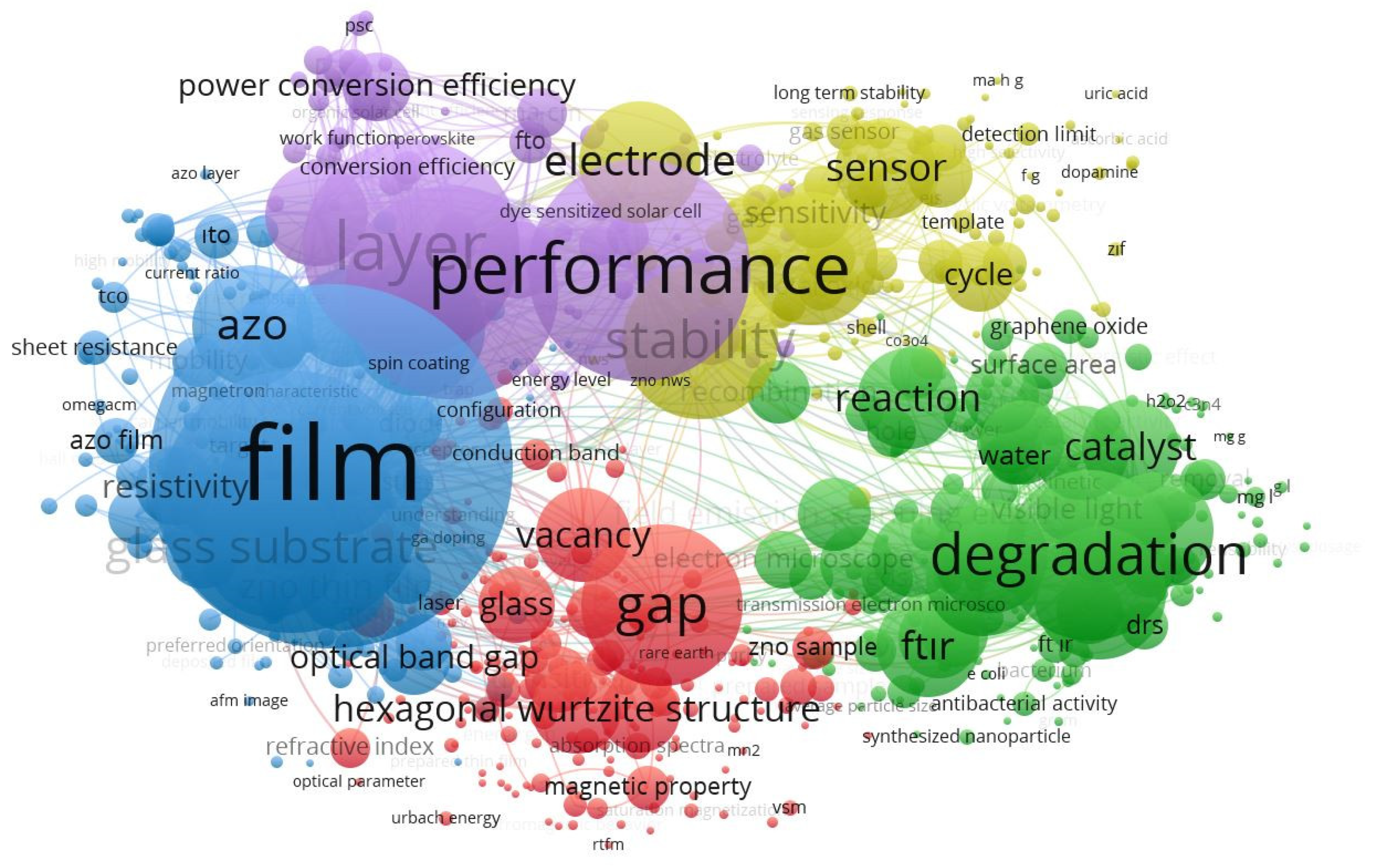
This study aims to examine the articles regarding In doped ZnO published in Web of Science database. The keywords "indium dope*" OR "in dope*" OR "influence of in dope*" OR "influence of indium dope*" OR "effect* of in dope*" OR "effect* of indium dope*" OR "addition of indium dope*" OR "addition of In dope*" AND “ZnO*” OR "zinc oxide" were entered to the “topic” sections and 900 articles were reached (31 March 2020). The language was selected as “English” and document type was fixed as “article”. Then, 777 articles were obtained for analysis. These articles were downloaded as tab-delimited (Win format) for the bibliometric analysis (full record and cited references format). The file was uploaded to VOSViewer programme in order to reveal the most used keywords, words in the abstracts, citation analyses, co-citation and co-authorship in countries analyses in the articles. The process of article selection is summarized in Figure 2.

3. Results

In order to create a map based on text data for the most used keywords, co-occurrence analysis was used and keywords were chosen by the selected authors. The minimum number of occurrences of a keyword was set as five, and the number of keywords to be selected was automatically obtained as 70. The map created is illustrated in Figure 3.
“ZnO” and “zinc oxide” are the most used keywords, as expected. These keywords were removed from the map to highlight the other most used keywords, which are: ‘photoluminescence’ (f = 47), “optical properties” (f = 44), “thin films” (f = 42) and “doping” (f = 38). Results indicate that the publications mostly focus on some characteristics of In doped ZnO thin films such as structural, optical and electrical features. Some of the studies related to In doped ZnO films grown by different techniques were analyzed, and IZO main features were reported in Table 1.
According to the studies reported in Table 1, the characteristics of ZnO depend on both growth technique and In doping content. In other words, ZnO, which is characterized by the hexagonal wurtzite structure, may exhibit different characteristics due to defects such as zinc interstitials and oxygen vacancies, which depend on the growth technique and growth parameters. Similar results were found also by many other authors [40,41]. Therefore, it can be suggested that the evaluation of ZnO’s characteristics should be made taking the growth technique into consideration. For example, in the studies [31,34], which investigate the variations in the characteristics of ZnO grown onto glass substrates by the ultrasonic spray pyrolysis technique as a function of In content, the authors found that samples generally have (002) crystallographic direction along c-axis. This preferential crystallization can be explained by the fact that the atoms have enough energy to spread to this region since the direction of the hexagonal ZnO structure (002) requires the lowest surface energy, so it can be thought that (002) orientation is the most optimal growth orientation for ZnO films [42,43,44]. On the other hand, for films grown by the spray pyrolysis technique, Prasada Rao and Santhoshkumar [45] found a highly oriented (100) ZnO crystallization. They explained this preferred orientation in terms of the amount of ethanol percentage, which affects the films’ crystallinity, the orientation of the crystallites in the films and the films’ morphology. The preferred orientation is explained in terms of nucleation and final growth orientation, both of which result from the nucleation at the film/substrate interface [46]. Similar interpretations were made by other researchers [47]. Other examples of the preferred orientation of ZnO depending on solution chemistry or growth technique are reported below. Dimitrov et al. [48] showed that if the solution is prepared by adding CH3COOH to the zinc ammonia precursor, ZnO with the (002) orientation can be obtained, while ZnO with the (100) orientation can be obtained if the zinc ammonia precursor is prepared with HNO3 or HCl. Additionally, it is possible to obtain ZnO films with a (101) preferred orientation by using RF magnetron sputtering. In summary, it can be said that many factors, such as substrate, heat treatment condition, solution chemistry, directly affect the crystallinity and thus the preferred orientation of the samples [49]. The most probable causes of the three possible orientations for ZnO are discussed above and presented to researchers as a preliminary information for future studies. However, it should be noted that the variation in the preferred orientation affects the properties of the samples. Therefore, it is very important to prepare ZnO to fit desirable purposes. For example, the dark current of ZnO obtained by the solution-based spray pyrolysis technique with a preferred orientation (100) displays a dark current smaller than (002) one [48]. In reference [48], authors found that ZnO films with orientation (100) reach the maximum dark current five seconds earlier than films with orientation (002), showing improved switching performances. Therefore, for researchers who want to examine the sensitivity of ZnO to ammonia, ethanol, acetone and water vapors, it may be suggested to grow ZnO films with preferred (100) orientation, which have much lower conductivity and are sensitive to vapor-based changes. After discussing the changes in preferred orientation, it is also necessary to mention the reasons for possible changes in peak intensity due to external doping. Peak intensity varies depending on indium doping. Fluctuations in the (002) peak appear as the result of deterioration of the crystal structure of ZnO due to In content. Defects induced by doping affect the structural, morphological, optical, electrical and magnetic properties of ZnO [50,51]. From the studies reported in Table 1, it can be observed that, in some cases, crystallite size increases with increasing In content, while in others an opposite tendency is observed. The differences between them can be summarized in terms of following possible reasons:
  • Factors, such as increase in the density of ZnO grains, the presence of elastic stress, the presence of In atoms as an interstitial atom in the ZnO crystal structure, lead to a decrease in the crystalline size of ZnO [31,37,38].
  • Generally, increasing crystallite size is linked with the ionic radii of the dopant and host ions. That is, increased crystallite sizes are likely to occur frequently, especially when larger atoms are used as the dopant. In this case, larger grains will be expected because hosted atoms with larger size replace the Zn atoms in the lattice. Additionally, some researchers mentioned that the morphology of the samples varies because of particle agglomeration due to indium content and therefore bigger particles were obtained [32,35,36,39,52].
It is known that In content and In dependent structural and morphological characteristics directly affect ZnO’s optoelectronic properties. As stated in the study of Hamberg and Granqvist [53], band-gap shift in a semiconductor is defined in terms of two competing mechanisms. The Burstein–Moss effect is generally used to define band-gap widening in heavily doped semiconductors, while electron–electron or electron–ion scattering is used for explaining band-gap narrowing [54,55]. The Burstein–Moss shift effect can be described as follow [56]:
  Δ E g B M = 2 2 m * ( 3 π 2 n ) 2
where n and m * are the carrier concentration and effective mass, respectively. From this Equation, it is possible to infer theoretically the Burstein-Moss shift, once known the carrier concentration. However, when the ZnO matrix is occupied by an ion belonging to the IIIB family, the electron concentration in ZnO increases. Similar to the study made by Cao et al. [55], the generation of free electrons in ZnO as a result of In doping can be expressed by using the following equations:
  Z n O Z n O 1 x + x 2   O 2 ( g )
  O O 1 2 O 2 ( g ) + V O
In Equation (2), Z n O 1 x x term takes into account the neutral oxygen vacancies V O   formed during the growth process of ZnO based on Equation (3). These neutrally formed oxygen vacancies may be singly ionized ( V O ) or doubly ionized ( V O ) , and are called paramagnetic and diamagnetic species, respectively. The occurrence of an electron as a result of single or doubly ionizing process may be described as follows [57]:
  V O V O + e
  V O V O + 2 e
where e is the electron in the conduction band of ZnO. From Equations (2–5), an interpretation on how to increase electron concentration in In doped ZnO can be made. Each Zn atom contributes 2/3 e to the adjacent O or O vacancy to achieve ZnO with n-type electrical conductivity. In this condition, if the Zn atom is substituted by In in the ZnO matrix, every In atom gives 3/3 e to the close O or O vacancy. Therefore, electron concentration increases because of In impurities in ZnO. From the aforementioned discussion, it can be concluded that if ZnO is doped with elements such as “In, Ga, Al Sn” belonging to IIIB and IVB of the periodic table, these elements act as donors, while IA group elements like Li act as acceptors. Therefore, the Burstein–Moss effect can be seen an effective way to explain the band-gap widening effect in ZnO as a result of the presence of In impurities. As mentioned before, the In addition-based defects level was mostly predicted using photoluminescence (PL) measurements. Generally, two emission peaks were observed in the PL spectra of ZnO. A strong peak is located at ~383 nm, while the weak one is located at ~550 nm. The broad peak located in the range of 500–600 nm can be associated with the non-stoichiometric intrinsic defects like zinc vacancies [58]. Moreover, there is a significant change in PL spectra of ZnO because of In doping. According to S.Y. Lim et al.’s [59] study, it can be observed that the intensity of UV emission is increased, while the peak shifts to higher wavelength as a result of increasing In content. This variation in visible luminescence can be related to defect induced emission resulting from increasing defect density. The broadening of the UV peak in PL spectra as a result of the indium addition can also be attributed to the band tail effect, which can be induced by indium impurities into the ZnO lattice.
It is well known that, in a transparent conductive oxide (TCO), the optical properties are strongly correlated to the electrical conductivity and both should be optimized for optoelectronic applications. Therefore, it is necessary to investigate the changes in electrical properties of ZnO films in terms of In content. This case is also seen in the cloud displayed in Figure 5. Additionally, in Figure 5, frequently passing keywords that indicate electrical properties of indium doped ZnO films, such as electrical property, device, carrier concentration, electrical resistivity and low resistivity, also indicate the importance of indium doped zinc oxide films in device applications. Most studies indicate that In doped ZnO films exhibit n-type electrical conductivity [60,61,62]. Additionally, the electrical conductivity of ZnO varies depending on the In content. For example, the sheet resistance of ZnO thin films obtained by Kumar et al. [63] by the chemical spray pyrolysis method was measured as 74 ohms/square and they associated this low resistance with the high amount of zinc metal found in ZnO (Zn/O ratio was 1.77). The electrical resistivity of ZnO films generally decreases with indium incorporation due to the increase in free electron concentration. That is, a large number of indium atoms can ionize in the form of In3+ and replace Zn2+ in the ZnO crystal structure, thereby contributing one free electron from each indium atom. The grain boundary scattering of electrons causes an increase in resistivity [22,61]. However, at high In contents, In segregation may occur and an increase in IZO resistance is observed [64,65]. This case is generally due to the fact that not all indium atoms contribute to conductivity with a free electron [66]. Additionally, similarly to Peng et al.’s study [67], increasing resistivity in higher indium doping content can be linked with the segregation of indium atoms in non-crystalline regions on the grain boundaries.
Table 2 compares the resistivity of In doped ZnO films obtained by different researchers with different techniques. Based on this, the lowest resistivity value for IZO films were obtained with the dc-reactive sputtering technique, while the highest resistivity value was obtained with the spray pyrolysis technique. Additionally, the resistivity value is related to the carrier concentration. In this sense, starting from the studies given in Table 2, it can be concluded that with the increase of In content (considering the doping rates to be determined depending on the technique used), the concentration of the electrical carrier increases and therefore the resistivity decreases.
Additionally, some studies report on resistivity increases at high In content. For example, Benouis et al. [35] found that IZO resistance tends to increase when In is higher than 2 at%, and that possible structural disorders occur as a result of doping. The authors explained the degradation of the electrical resistivity as due to the accumulation of In in indium hydroxide In(OH)3 forming at the grain boundaries, and to the fact that chlorine functions as a trap for electrons [76]. In addition, similarly to what occurs in other TCOs, by increasing film thickness, the concentration of charge carriers increases, thus increasing the conductivity of the material and reducing its transparency. Therefore, an optimal compromise must be acquired between optical transparency and electrical conductivity, with the optical and electrical characteristics correlated with an inverse relationship. It would be preferable to increase the thickness rather than increasing the doping level of a TCO, in order to decrease the sheet resistance of the film while maintaining free carrier absorption as low as possible.
The effect of post deposition annealing on the optical and electrical properties of IZO films has been investigated by several authors. For instance, Guo-Ping et al. [77] found that deposited IZO films grown by RF sputtering have carrier concentrations in the range of 1019 cm−3, which increased up to 4.37 × 1020 cm−3 with a 30 min annealing treatment at 450 °C in argon atmosphere. As a result of this, they obtained IZO films with 2.5 × 10⁻³ Ωcm resistivity. Additionally, Barquinha et al. [78] found a decrease of the electrical resistivity of IZO films upon annealing. However, there are many other works reporting on the increase of IZO films resistance as a result of annealing [70]. Moreover, considering the studies reported in Table 1 and Table 2, it may be observed that samples grown with the same method by different authors have different characteristics. Samples prepared by chemical synthesis may have different precursor solutions and different dopant concentrations, which lead to different electrical and optical properties. For films deposited by Physical Vapour Deposition techniques, several growth parameters (sputtering pressure, oxygen partial pressure, substrate temperature, target to substrate distance, RF or DC powers, magnetron, etc.) affect films’ performances. From the analyzed works, we can summarize that best film performances are achieved generally by physical vapor deposition (PVD) techniques. In addition, differences may also occur in ZnO-based devices. For example, diodes fabricated in the same way may have different diode characteristics, due to different thicknesses of the oxide layer in the metal semiconductor interface and/or due to the non-homogeneous distribution of ZnO as the interface layer [79]. The above-mentioned discussion shows the variety of characteristics of indium doped zinc oxide films, and analyzes the possible reasons, providing time-saving information for guiding the researchers’ studies.
In doped ZnO studies began to grow in number in 2010, though the first study was published on the Web of Science much earlier, in 1976. When the distribution of the number of articles using the keywords by year is shown, it can be seen that recent articles focus mainly on the synthesis of In doped ZnO film via different techniques such as sol-gel and the hydrothermal route, and on device applications such as solar cell and gas sensors. The distribution of the number of the articles by years is presented in Figure 4. The 2016 value in Figure 4 indicates the point of increase of the used-keyword number in articles up to the present. From the analysis of the publications on In doped ZnO, we found that IZO films are mostly used in diode applications, gas sensors and solar cells. Figure 4 shows the emergence of studies on nanoparticles, nanorods and gas sensors in the last few years, together with the advance of low-cost chemical routes such as hydrothermal, sol-gel and spray pyrolysis techniques. This allows us to predict the trends in future studies which will be focused on IZO films and nanostructures obtained by low-cost synthesis for gas sensor and optoelectronic applications.
In order to create a map based on text data for the most used words in the abstracts of articles, the Web of Science bibliographic database file was uploaded into the program. Subsequently, the abstract and binary counting method was selected as the field. The minimum number of occurrences of a term was set as 20 and the number of terms to be selected was automatically stated to be 98. The map created from this is reported in Figure 5.
Figure 5 shows three clusters, and the words “film” (f = 327) and “thin film” (f = 185) are the most used words found in the abstracts. The most used words were also found to be: X-ray diffraction (f = 146), glass substrate (f = 135), X-ray Diffraction (XRD) (f = 135), spectra (f = 131) and layer (f = 128). From these results, it can be concluded that research on In doped ZnO generally focuses on its synthesis and characterization in its thin film form. In addition, the high number of words: glass, XRD, spectra and layer indicate that In-doped ZnO films are synthesized for use in different applications and XRD and spectral techniques are often used for their characterization. On the contrary, the frequency of the words “X-ray photoelectron spectroscopy (XPS), atomic force microscopy (AFM), Photoluminescence Spectroscopy (PL), energy dispersive x-ray spectroscopy (EDS)” was found to be less than the others. Therefore, it is recommended that researchers use these analyses in their studies. Considering that the size of the circles in Figure 5 depends on the frequency of the words in the abstract, it can be concluded that research on nano-shapes regarding In-doped ZnO is limited in this field. Additionally, the frequency of words such as “SEM”,” electron microscopy”, “nanostructure”, “nanoparticle”, “nanorod”, “nanowire”, “morphology”, which indicate the analysis of different IZO morphology, was 71, 70, 46, 68, 47, 41 and 121, respectively. Nevertheless, the ZnO nanostructures have taken the lead in recent years thanks to advanced synthesis methods, and the number of publications about ZnO nanostructures is lower in comparison with those on thin films, and the relationship of the above mentioned words (SEM, nanoparticles, etc.) with the other keywords is weak, which explains their relevance observed in the charts. Therefore, it is important for researchers to study this subject to fill the gap in the field. Additionally, the words “device”, “layer” and “thickness” indicated that In doped ZnO films have also been used in device applications as interlayer structures. Thus, it is recommended that the authors concentrate on studies investigating the performance of nano-shaped indium doped ZnO structures for device applications.
When the distribution of the most used words is shown on a year-by-year basis, it is evident that more recent articles tend to focus on the efficiency and performance of In doped ZnO films as well as TCO in device applications such as solar cells, diodes and photoluminescence applications. The distribution of the most used words in abstracts by year is presented in Figure 6. The 2014 value in Figure 6 indicates the point of increase of the used-words number in abstracts up to the present. Accordingly, the effect of nanoparticles, variation in crystallite size and morphology are the most examined features of In doped ZnO films in aforementioned device applications.
In order to create a map for most cited authors, citation analysis and authors were selected. The minimum number of documents by a particular author was set as five and the minimum number of citations of an author was determined as 10. The number of authors to be selected was automatically obtained as 25. The map created is shown in Figure 7. This indicates that Maldonado (384 citations) and Asomoza (286 citations) were the most cited authors in this field.
Examining the reference analysis of Maldonado’s studies on Indium doped ZnO on Web of Science database, it is observed that articles titled "Indium-doped ZnO thin films deposited by the sol-gel technique [80]” and “Characterization of indium-doped zinc oxide films deposited by pyrolytic spray with different indium compounds as dopant [81]” have the most citations. Both studies were published in the "Thin Solid Film" journal. Researchers can use these studies as a source for their studies.
In addition, the co-citation analysis and cited authors were selected. The minimum number of citations of an author was set as 30 and the number of authors to be selected was automatically given as 44. The map created is shown in Figure 8. The co-citation analysis shows us the most cited authors in the reference list sections of the articles that were included in the analysis. It shows that Major (99 citations), Minami (87 citations) and Ozgur (85 citations) are most co-cited authors in this field. It can be said that these authors are leaders in the studies regarding In doped ZnO. Analyzing the studies of these authors will contribute to researchers’ future studies on this subject.
In order to create a map for most cited journals, the citation analysis and sources were selected. The minimum number of documents of a source was set as five and the minimum number of citations of a source was also set as five. The number of sources to be selected was automatically obtained as 43. The map created from this is presented in Figure 9. Figure 9 shows that the most cited journals are “Thin Solid Films (2434 citations, 49 documents), Sensors” and “Actuators B: Chemical (720 citations, 8 documents)” and “Applied Physics Letters (680 citations, 15 documents)”.
Examining the reference analysis of “Thin Solid Films” on Indium doped ZnO on the Web of Science database, it is observed that articles titled "Zinc oxide thin films by the spray pyrolysis method [82]” and “Highly Transparent and Conducting Indium-Doped Zinc-Oxide Films by Spray Pyrolysis [83]” have the most citations. Both studies were published in the "Thin Solid Film" journal. Researchers can use these studies as a source in their future studies.
In addition to the citation analysis stated in the Figure 9, the number of articles in journals was also analyzed by years. Although the number of publications in “Thin Solid Film” is high, in recent years this journal has lost its popularity in regards to publications on In doped ZnO. It is seen that “Solar Energy”, “Ceramics International”, “Applied Physics-A”, “Optik”, “Material Research Express”, “ACS Applied Materials and Interfaces”, and “Optical Materials” published more studies since 2016 to the present. Therefore, it is suggested that these journals are preferred in future studies. The graph of all these results is presented in Figure 10.
In addition, the co-citation analysis and cited sources were selected. The minimum number of citations of a source was set at 30 and the number of sources to be selected was automatically stated to 127. Figure 11 shows the resulting map. It shows that the most co-cited journals are “Applied Physics Letters” (2084 co-citations), “Thin Solid Films” (1624 co-citations), “Journal of Applied Physics” (1400 co-citations), “Physical Review B” (975 co-citations), and “Applied Surface Science” (626 co-citations). It is indicated that these journals are leaders in regards to their studies on In doped ZnO.
When the citation analysis of the studies on indium doped ZnOs on the Web of Science database in “Applied Physics Letters” is examined, it is seen that the studies named "Large and abrupt optical band gap variation in In-doped ZnO [84]" and "ZnO nanowires and nanobelts: Shape selection and thermodynamic modeling [85]" received more citations than the others. Authors may use these studies as important bibliographic sources.
In order to create a map for co-authorship in countries, co-authorship and countries were selected. The minimum number of documents of a source of a country was adjusted as five and the minimum number of citations from a country was stated as five. The number of countries to be selected was automatically stated as 34. The created map is shown in Figure 12. Figure 12 shows that the countries with the higher number of documents are China (Citations = 4105, Documents = 177), India (Citations = 2104, Documents = 124), South Korea (Citations = 2268, Documents = 93), USA (Citations = 1573, Documents = 69), Taiwan (Citations = 681, Documents = 40) and Japan (Citations = 676, Documents = 39).
According to the results, it is seen that China and India are the leading countries in this field, while in Mexico, Australia, Austria, Ukraine, Thailand, Egypt, Belgium, Netherlands, Iraq and Morocco, the studies on indium doped ZnO are very few. In this context, it is recommended that these countries collaborate with the leading countries in the field (China and India) to produce more publications.

4. Conclusions

In this study, a bibliometric analysis was conducted in order to reveal relationships between concepts in keywords and abstracts, the most cited/co-cited authors, the most cited/co-cited journals and the countries with the most academic studies in In doped ZnO studies. Results show that, apart from the obvious most used keywords such as ZnO and zinc oxide, photoluminescence, optical properties, thin films and doping are the other most used keywords. In addition, film, thin film, X-ray diffraction, glass substrate, XRD, and spectra are the most used words found in the abstracts. When the distribution of the words is searched on a year-by-year basis, it is evident that more recent articles tend to focus on efficiency and performance of In doped ZnO films as TCO in device applications such as solar cells, diodes, gas sensors and photoluminescence applications. The analysis of recent publications also shows an increasing interest towards IZO nanostructures (nanoparticles, nanorods, etc.) obtained by low cost chemical routes. Citation analysis reveals that Maldonado and Asomoza are the most cited authors, and Major, Minami and Ozgur are the most co-cited authors in this field. Thin Solid Films, Sensors and Actuators B: Chemical, Applied Physics Letters are the most cited journals and the most co-cited journals are Applied Physics Letters, Thin Solid Films, Journal of Applied Physics, Physical Review, Applied Surface Science. Finally, the countries with the highest number of documents are China, India, South Korea, USA and Japan, respectively. Based on all of our results and literature discussion, suggestions for authors are presented below:
  • The studies mostly focus on some characteristics of In doped ZnO thin films such as structural, optical and electrical features. It is suggested that authors also pay attention to studies on the magnetic properties of ZnO. It is advised that the evaluation of ZnO’s characteristics should also be made taking growth techniques into consideration.
  • For researchers who want to examine the sensitivity of ZnO to ammonia, ethanol, acetone and water vapors, it may be suggested to work with (100) directed ZnO films due to the fact that films with (100) preferred orientation have much higher conductivity and higher sensing performance.
  • Research on In doped ZnO generally focuses on its synthesis and characterization in its thin film form. However, studies on In-doped ZnO nanostructures are limited. Therefore, it is important for researchers to study this subject to fill the gap in the field.
  • In doped ZnO films have been used in device applications as interlayer structures. Thus, it is recommended that the authors should concentrate on studies investigating the performance of non-shaped indium doped ZnO structures in device applications.
  • Maldonado’s studies on Indium doped ZnO entitled "Indium-doped ZnO thin films deposited by the sol-gel technique [63]” and “Characterization of indium-doped zinc oxide films deposited by pyrolytic spray with different indium compounds as dopant [64]” have the most citations. Researchers can use these studies and can also examine other works published in the same journal.
  • The studies of Major, Minami and Ozgur could contribute to researchers’ future studies on this subject. Researchers can use these studies as a relevant source in future studies.
  • Articles entitled "Zinc oxide thin films by the spray pyrolysis method [65]” and “Highly Transparent and Conducting Indium-Doped Zinc-Oxide Films by Spray Pyrolysis [66]” have more citations than the others in Thin Solid Films. Researchers can use these studies as a source reference in future studies.
  • Applied Physics Letters, Thin Solid Films, Journal of Applied Physics, Physical Review, Applied Surface Science are leader journals with their studies on IZO. However, Solar Energy, Ceramics International, Applied Physics-A, Optik, Material Research Express, ACS Applied Materials and Interfaces, Optical Materials published more studies from 2016 to the present. Therefore, it is suggested that all these journals can contribute to the future study of the researchers on this subject.
  • The studies entitled "Large and abrupt optical band gap variation in In-doped ZnO [67]" and "ZnO nanowires and nanobelts: Shape selection and thermodynamic modeling [68]" received more citations than others in the Applied Physics Letters. Authors could use these studies as a main source when writing a literature discussion in their future works.
  • The countries with the highest number of documents on In doped ZnO are China, India, South Korea, USA and Japan. Researchers working in this field can undertake post-doctoral studies in the aforementioned countries. In addition, international projects can be produced by collaborating with these countries.
  • In Mexico, Australia, Austria, Ukraine, Thailand, Egypt, Belgium, Netherlands, Iraq and Morocco, it is seen that the studies on indium doped ZnO are very few. It is recommended that these countries collaborate with the leading countries in the field (China and India) to produce more publications.

Author Contributions

Methodology, M.Y.; writing—original draft preparation, M.L.G.; writing—review and editing, G.T. All authors have read and agreed to the published version of the manuscript.

Funding

This research received no external funding.

Acknowledgments

The authors would like to thank Rabia Meryem Yilmaz from Ataturk University, Department of Computer Education and Instructional Technology for her valuable contributions to this study.

Conflicts of Interest

The authors declare no conflict of interest.

References

  1. Ranu, B.C.; Mandal, T. Indium(I) Iodide-Promoted Cleavage of Diaryl Diselenides and Disulfides and Subsequent Condensation with Alkyl or Acyl Halides. One-Pot Efficient Synthesis of Diorganyl Selenides, Sulfides, Selenoesters, and Thioesters. J. Org. Chem. 2004, 69, 5793–5795. [Google Scholar] [CrossRef] [PubMed]
  2. Schneider, U.; Dao, H.T.; Kobayashi, S. Unusual Carbon−Carbon Bond Formations between Allylboronates and Acetals or Ketals Catalyzed by a Peculiar Indium(I) Lewis Acid. Org. Lett. 2010, 12, 2488–2491. [Google Scholar] [CrossRef] [PubMed]
  3. Habashi, F. Indium, Physical and Chemical Properties. In Encyclopedia of Metalloproteins; Springer: New York, NY, USA, 2013; pp. 981–982. [Google Scholar]
  4. Choubey, P.K.; Jha, M.K.; Gupta, D.; Jeong, J.; Lee, J.-C. Recovery of Rare Metal Indium (In) from Discarded LCD Monitors. In Rare Metal Technology 2014; John Wiley & Sons, Inc.: Hoboken, NJ, USA, 2014; pp. 37–42. ISBN 9781118888827. [Google Scholar]
  5. Hofmann, M.; Hofmann, H.; Hagelüken, C.; Hool, A. Critical raw materials: A perspective from the materials science community. Sustain. Mater. Technol. 2018, 17, e00074. [Google Scholar] [CrossRef]
  6. European Commıssıon Commıttee and the Commıttee of the Regıons on the 2017 list of Critical Raw Materials for the EU. Commun. From Comm. Eur. Parliam. Counc. Eur. Econ. Soc. Comm. Comm. Reg. 2017, XIV, 293.
  7. Yilmaz, M.; Grilli, M.L. The modification of the characteristics of nanocrystalline ZnO thin films by variation of Ta doping content. Philos. Mag. 2016, 96, 2125–2142. [Google Scholar] [CrossRef]
  8. Yilmaz, M.; Tatar, D.; Sonmez, E.; Cirak, C.; Aydogan, S.; Gunturkun, R. Investigation of Structural, Morphological, Optical, and Electrical Properties of Al Doped ZnO Thin Films Via Spin Coating Technique. Synth. React. Inorganic, Met. Nano-Metal Chem. 2016, 46, 489–494. [Google Scholar] [CrossRef]
  9. Yilmaz, M.; Turgut, G.; Aydin, S.; Ertugrul, M. Electrochemical deposition of ZnO thin films on to tin(IV) oxide:Fluorine. Asian J. Chem. 2012, 24, 3371–3374. [Google Scholar]
  10. Sun, X.; Li, Q.; Jiang, J.; Mao, Y. Morphology-tunable synthesis of ZnO nanoforest and its photoelectrochemical performance. Nanoscale 2014, 6, 8769–8780. [Google Scholar] [CrossRef]
  11. Kahraman, S.; Çakmak, H.M.; Çetinkaya, S.; Bayansal, F.; Çetinkara, H.A.; Güder, H.S. Characteristics of ZnO thin films doped by various elements. J. Cryst. Growth 2013, 363, 86–92. [Google Scholar] [CrossRef]
  12. Nunes, P.; Braz Fernandes, F.M.; Silva, R.J.C.; Fortunato, E.; Martins, R. Structural Characterisation of Zinc Oxide Thin Films Produced by Spray Pyrolysis. Key Eng. Mater. 2002, 230, 599–602. [Google Scholar] [CrossRef]
  13. Rashed, H.A.; Umran, N.M. The stability and electronic properties of Si-doped ZnO nanosheet: A DFT study. Mater. Res. Express 2019, 6, 045044. [Google Scholar] [CrossRef]
  14. Habashyani, S.; Özmen, A.; Aydogan, S.; Yilmaz, M. An examination of correlation between characteristic and device performance of ZnO films as a function of La content. Vacuum 2018, 157, 497–507. [Google Scholar] [CrossRef]
  15. Feng, T.-H.; Xia, X.-C. Characteristics of doping controllable ZnO films grown by photo-assisted metal organic chemical vapor deposition. Opt. Mater. Express 2017, 7, 1281. [Google Scholar] [CrossRef]
  16. Sukee, A.; Kantarak, E.; Singjai, P. Preparation of Aluminum doped Zinc Oxide Thin Films on Glass Substrate by Sparking Process and Their Optical and Electrical Properties. J. Phys. Conf. Ser. 2017, 901, 012153. [Google Scholar] [CrossRef]
  17. Arici, F.; Yildirim, P.; Caliklar, Ş.; Yilmaz, R.M. Research trends in the use of augmented reality in science education: Content and bibliometric mapping analysis. Comput. Educ. 2019, 142, 103647. [Google Scholar] [CrossRef]
  18. Yilmaz, R.M.; Topu, F.B.; Takkaç Tulgar, A. An examination of the studies on foreign language teaching in pre-school education: A bibliometric mapping analysis. Comput. Assist. Lang. Learn. 2019, 1–24. [Google Scholar] [CrossRef]
  19. Liao, H.; Tang, M.; Luo, L.; Li, C.; Chiclana, F.; Zeng, X.-J. A Bibliometric Analysis and Visualization of Medical Big Data Research. Sustainability 2018, 10, 166. [Google Scholar] [CrossRef] [Green Version]
  20. Melkers, J. Bibliometrics as a Tool for Analysis of R&D Impacts. In Evaluating R&D Impacts: Methods and Practice; Springer: Boston, MA, USA, 1993; pp. 43–61. [Google Scholar]
  21. Silva-Lopez, H.E.; Marcelino, B.S.; Guillen-Cervantes, A.; Zelaya-Angel, O.; Ramirez-Bon, R. Physical Properties of Sputtered Indium-doped ZnO Films Deposited on Flexible Transparent Substrates. Mater. Res. 2018, 21, 1–6. [Google Scholar] [CrossRef] [Green Version]
  22. Biswal, R.; Maldonado, A.; Vega-Pérez, J.; Acosta, D.R.; De La Luz Olvera, M. Indium Doped Zinc Oxide Thin Films Deposited by Ultrasonic Chemical Spray Technique, Starting from Zinc Acetylacetonate and Indium Chloride. Materials 2014, 7, 5038–5046. [Google Scholar] [CrossRef] [Green Version]
  23. Du, X.; Liu, B.; Li, L.; Kong, X.; Zheng, C.; Lin, H.; Tong, Q.; Tao, S.; Zhang, X. Excimer emission induced intra-system self-absorption enhancement – a novel strategy to realize high efficiency and excellent stability ternary organic solar cells processed in green solvents. J. Mater. Chem. A 2018, 6, 23840–23855. [Google Scholar] [CrossRef]
  24. Ting, C.-C.; Chang, S.-P.; Li, W.-Y.; Wang, C.-H. Enhanced performance of indium zinc oxide thin film transistor by yttrium doping. Appl. Surf. Sci. 2013, 284, 397–404. [Google Scholar] [CrossRef]
  25. Moradi-Haji Jafan, M.; Zamani-Meymian, M.-R.; Rahimi, R.; Rabbani, M. The effect of solvents and the thickness on structural, optical and electrical properties of ITO thin films prepared by a sol–gel spin-coating process. J. Nanostructure Chem. 2014, 4, 89. [Google Scholar] [CrossRef] [Green Version]
  26. Wade, K.; Banister, A. The Chemistry of Aluminium, Gallium, Indium and Thallium: Comprehensive Inorganic Chemistry; Pergamon Press: Oxford, UK, 2016. [Google Scholar]
  27. Shaheera, M.; Girija, K.G.; Kaur, M.; Geetha, V.; Debnath, A.K.; Vatsa, R.K.; Muthe, K.P.; Gadkari, S.C. Characterization and device application of indium doped ZnO homojunction prepared by RF magnetron sputtering. Opt. Mater. 2020, 101, 109723. [Google Scholar] [CrossRef]
  28. Yu, Y.; Yao, B.; He, Y.; Cao, B.; Ma, W.; Chang, L. Oxygen defect-rich In-doped ZnO nanostructure for enhanced visible light photocatalytic activity. Mater. Chem. Phys. 2020, 244, 122672. [Google Scholar] [CrossRef]
  29. Bhatia, S.; Verma, N. Gas Sensing Performance of Dip-Coated Indium-Doped ZnO Films. J. Electron. Mater. 2018, 47, 6450–6457. [Google Scholar] [CrossRef]
  30. Kyaw, A.K.K.; Wang, Y.; Zhao, D.W.; Huang, Z.H.; Zeng, X.T.; Sun, X.W. The properties of sol-gel processed indium-doped zinc oxide semiconductor film and its application in organic solar cells. Phys. Status Solidi 2011, 208, 2635–2642. [Google Scholar] [CrossRef]
  31. El Filali, B.; Jaramillo Gomez, J.A.; Torchynska, T.V.; Casas Espinola, J.L.; Shcherbyna, L. Band-edge emission, defects, morphology and structure of in-doped ZnO nanocrystal films. Opt. Mater. 2019, 89, 322–328. [Google Scholar] [CrossRef]
  32. Khalfallah, B.; Chaabouni, F.; Abaab, M. Some physical investigations on In-doped ZnO films prepared by RF magnetron sputtering using powder compacted target. J. Mater. Sci. Mater. Electron. 2015, 26, 5209–5216. [Google Scholar] [CrossRef]
  33. Thambidurai, M.; Kim, J.Y.; Kang, C.M.; Muthukumarasamy, N.; Song, H.J.; Song, J.; Ko, Y.; Velauthapillai, D.; Lee, C. Enhanced photovoltaic performance of inverted organic solar cells with In-doped ZnO as an electron extraction layer. Renew. Energy 2014, 66, 433–442. [Google Scholar] [CrossRef]
  34. Benhaliliba, M.; Benouis, C.E.; Mouffak, Z.; Ocak, Y.S.; Tiburcio-Silver, A.; Aida, M.S.; Garcia, A.A.; Tavira, A.; Sanchez Juarez, A. Preparation and characterization of nanostructures of in-doped ZnO films deposited by chemically spray pyrolysis: Effect of substrate temperatures. Superlattices Microstruct. 2013, 63, 228–239. [Google Scholar] [CrossRef]
  35. Benouis, C.E.; Benhaliliba, M.; Sanchez Juarez, A.; Aida, M.S.; Chami, F.; Yakuphanoglu, F. The effect of indium doping on structural, electrical conductivity, photoconductivity and density of states properties of ZnO films. J. Alloys Compd. 2010, 490, 62–67. [Google Scholar] [CrossRef]
  36. Lee, C.; Lim, K.; Song, J. Highly textured ZnO thin films doped with indium prepared by the pyrosol method. Sol. Energy Mater. Sol. Cells 1996, 43, 37–45. [Google Scholar] [CrossRef]
  37. Rambu, A.P.; Sırbu, D.; Sandu, A.V.; Prodan, G.; Nıca, V. Influence of In doping on electro-optical properties of ZnO films. Bull. Mater. Sci. 2013, 36, 231–237. [Google Scholar] [CrossRef]
  38. Tang, K.; Gu, S.; Liu, J.; Ye, J.; Zhu, S.; Zheng, Y. Effects of indium doping on the crystallographic, morphological, electrical, and optical properties of highly crystalline ZnO films. J. Alloys Compd. 2015, 653, 643–648. [Google Scholar] [CrossRef]
  39. Jongthammanurak, S.; Cheawkul, T.; Witana, M. Morphological differences in transparent conductive indium-doped zinc oxide thin films deposited by ultrasonic spray pyrolysis. Thin Solid Film. 2014, 571, 114–120. [Google Scholar] [CrossRef]
  40. ILICAN, S.; İlgü Büyük, G. ZnO:Eu Filmlerinin Mikroyapısal ve Optik Özellikleri. Karadeniz Fen Bilim. Derg. 2018, 8, 141–153. [Google Scholar] [CrossRef]
  41. Marouf, S.; Beniaiche, A.; Guessas, H.; Azizi, A. Morphological, Structural and Optical Properties of ZnO Thin Films Deposited by Dip Coating Method. Mater. Res. 2016, 20, 88–95. [Google Scholar] [CrossRef] [Green Version]
  42. Karakaya, S. Annealing Effect on Structural and Optical Properties of ZnO Films Prepared by Ultrasonic Spray Pyrolysis. ANADOLU Univ. J. Sci. Technol. A Appl. Sci. Eng. 2016, 17, 670–676. [Google Scholar] [CrossRef] [Green Version]
  43. Purohit, A.; Chander, S.; Sharma, A.; Nehra, S.P.; Dhaka, M.S. Impact of low temperature annealing on structural, optical, electrical and morphological properties of ZnO thin films grown by RF sputtering for photovoltaic applications. Opt. Mater. 2015, 49, 51–58. [Google Scholar] [CrossRef]
  44. Ye, J.; Gu, S.; Zhu, S.; Chen, T.; Hu, L.; Qin, F.; Zhang, R.; Shi, Y.; Zheng, Y. The growth and annealing of single crystalline ZnO films by low-pressure MOCVD. J. Cryst. Growth 2002, 243, 151–156. [Google Scholar] [CrossRef]
  45. Prasada Rao, T.; Santhoshkumar, M.C. Highly oriented (100) ZnO thin films by spray pyrolysis. Appl. Surf. Sci. 2009, 255, 7212–7215. [Google Scholar] [CrossRef]
  46. Francombe, M.H.; Satō, H. Single Crystal Films; Pergamon Press: London, UK, 1964. [Google Scholar]
  47. Ilıcan, S.; Çağlar, Y.; Çağlar, M. X-ray Diffraction Studies of Undoped and in-Doped Cd0.22Zn0.78S Films Deposited by Spray Pyrolysis. Cankaya Univ. J. Arts Sci. 2005, 1, 85–94. [Google Scholar]
  48. Dimitrov, O.; Nesheva, D.; Blaskov, V.; Stambolova, I.; Vassilev, S.; Levi, Z.; Tonchev, V. Gas sensitive ZnO thin films with desired (002) or (100) orientation obtained by ultrasonic spray pyrolysis. Mater. Chem. Phys. 2014, 148, 712–719. [Google Scholar] [CrossRef]
  49. Kumar, V.; Singh, N.; Mehra, R.M.; Kapoor, A.; Purohit, L.P.; Swart, H.C. Role of film thickness on the properties of ZnO thin films grown by sol-gel method. Thin Solid Films 2013, 539, 161–165. [Google Scholar] [CrossRef]
  50. Liu, F.-C.; Li, J.-Y.; Chen, T.-H.; Chang, C.-H.; Lee, C.-T.; Hsiao, W.-H.; Liu, D.-S. Effect of Silver Dopants on the ZnO Thin Films Prepared by a Radio Frequency Magnetron Co-Sputtering System. Materials 2017, 10, 797. [Google Scholar] [CrossRef]
  51. Obeid, M.M.; Jappor, H.R.; Al-Marzoki, K.; Al-Hydary, I.A.; Edrees, S.J.; Shukur, M.M. Unraveling the effect of Gd doping on the structural, optical, and magnetic properties of ZnO based diluted magnetic semiconductor nanorods. RSC Adv. 2019, 9, 33207–33221. [Google Scholar] [CrossRef] [Green Version]
  52. Khashan, K.S.; Mahdi, M. Preparation of indium-doped zinc oxide nanoparticles by pulsed laser ablation in liquid technique and their characterization. Appl. Nanosci. 2017, 7, 589–596. [Google Scholar] [CrossRef] [Green Version]
  53. Hamberg, I.; Granqvist, C.G. Evaporated Sn-doped In 2O3 films: Basic optical properties and applications to energy-efficient windows. J. Appl. Phys. 1986, 60, R123–R160. [Google Scholar] [CrossRef]
  54. Singh, A.; Chaudhary, S.; Pandya, D.K. High conductivity indium doped ZnO films by metal target reactive co-sputtering. Acta Mater. 2016, 111, 1–9. [Google Scholar] [CrossRef]
  55. Cao, Y.; Miao, L.; Tanemura, S.; Tanemura, M.; Kuno, Y.; Hayashi, Y.; Mori, Y. Optical Properties of Indium-Doped ZnO Films. Jpn. J. Appl. Phys. 2006, 45, 1623–1628. [Google Scholar] [CrossRef]
  56. Aydoğan, Ş.; Grilli, M.L.; Yilmaz, M.; Çaldiran, Z.; Kaçuş, H. A facile growth of spray based ZnO films and device performance investigation for Schottky diodes: Determination of interface state density distribution. J. Alloys Compd. 2017, 708, 55–66. [Google Scholar] [CrossRef]
  57. Lim, J.H.; Lee, S.M.; Kim, H.-S.; Kim, H.Y.; Park, J.; Jung, S.-B.; Park, G.C.; Kim, J.; Joo, J. Synergistic effect of Indium and Gallium co-doping on growth behavior and physical properties of hydrothermally grown ZnO nanorods. Sci. Rep. 2017, 7, 41992. [Google Scholar] [CrossRef] [PubMed] [Green Version]
  58. Kim, Y.-S.; Tai, W.-P.; Shu, S.-J. Effect of preheating temperature on structural and optical properties of ZnO thin films by sol–gel process. Thin Solid Films 2005, 491, 153–160. [Google Scholar] [CrossRef]
  59. Lim, S.Y.; Brahma, S.; Liu, C.-P.; Wang, R.-C.; Huang, J.-L. Effect of indium concentration on luminescence and electrical properties of indium doped ZnO nanowires. Thin Solid Film. 2013, 549, 165–171. [Google Scholar] [CrossRef]
  60. Hori, Y.; Shiota, Y.; Ida, T.; Yoshizawa, K.; Mizuno, M. Local structures and electronic properties of In atoms in In-doped ZnO. Thin Solid Film. 2019, 685, 428–433. [Google Scholar] [CrossRef]
  61. Chirakkara, S.; Nanda, K.K.; Krupanidhi, S.B. Pulsed laser deposited ZnO: In as transparent conducting oxide. Thin Solid Films 2011, 519, 3647–3652. [Google Scholar] [CrossRef]
  62. Caglar, M.; Caglar, Y.; Ilican, S. Electrical and optical properties of undoped and In-doped ZnO thin films. Phys. Status Solidi c 2007, 4, 1337–1340. [Google Scholar] [CrossRef]
  63. Kumar, P.M.R.; Kartha, C.S.; Vijayakumar, K.P.; Abe, T.; Kashiwaba, Y.; Singh, F.; Avasthi, D.K. On the properties of indium doped ZnO thin films. Semicond. Sci. Technol. 2004, 20, 120–126. [Google Scholar] [CrossRef]
  64. Edinger, S.; Bansal, N.; Bauch, M.; Wibowo, R.A.; Újvári, G.; Hamid, R.; Trimmel, G.; Dimopoulos, T. Highly transparent and conductive indium-doped zinc oxide films deposited at low substrate temperature by spray pyrolysis from water-based solutions. J. Mater. Sci. 2017, 52, 8591–8602. [Google Scholar] [CrossRef] [Green Version]
  65. Caglar, Y.; Zor, M.; Caglar, M.; Ilican, S. Influence of the indium incorporation on the structural and electrical properties of zinc oxide films. J. Optoelectron. Adv. Mater. 2006, 8, 1867–1873. [Google Scholar]
  66. Nasir, M.F.; Hannas, M.; Mamat, M.H.; Rusop, M. Electrical Properties of Indium-Doped Zinc Oxide Nanostructures Doped at Different Dopant Concentrations. In Proceedings of the Nanoscience, Nanotechnology and Nanoengineering: Fundamentals and Applications; Trans Tech Publications Ltd.: Baech, Switzerland, 2015; Volume 1109, pp. 593–597. [Google Scholar]
  67. Peng, L.; Fang, L.; Zhao, Y.; Wu, W.; Ruan, H.; Kong, C. Growth and characterization of indium doped zinc oxide films sputtered from powder targets. J. Wuhan Univ. Technol. Sci. Ed. 2017, 32, 866–870. [Google Scholar] [CrossRef]
  68. Mahesh, D.; Kumar, M.C.S. Synergetic effects of aluminium and indium dopants in the physical properties of ZnO thin films via spray pyrolysis. Superlattices Microstruct. 2020, 142, 106511. [Google Scholar] [CrossRef]
  69. Benzitouni, S.; Zaabat, M.; Mahdjoub, A.; Benaboud, A.; Boudine, B. High transparency and conductivity of heavily In-doped ZnO thin films deposited by dip-coating method. Mater. Sci. 2018, 36, 427–434. [Google Scholar] [CrossRef] [Green Version]
  70. Ullah, M.; Chunlei, W.; Su, W.-B.; Manan, A.; Ahmad, A.S.; Rehman, A.U. Thermoelectric properties of indium-doped zinc oxide sintered in an argon atmosphere. J. Mater. Sci. Mater. Electron. 2019, 30, 4813–4818. [Google Scholar] [CrossRef]
  71. Winkler, N.; Wibowo, A.; Kubicek, B.; Kautek, W.; Ligorio, G.; List-Kratochvil, E.; Dimopoulos, T. Rapid Processing of In-Doped ZnO by Spray Pyrolysis from Environment-Friendly Precursor Solutions. Coatings 2019, 9, 245. [Google Scholar] [CrossRef] [Green Version]
  72. Mahesh, D.; Kumar, B.H.; Kumar, M.C.S. Enhanced luminescence property of 1 D nanorods realised by aqueous chemical growth on indium doped zinc oxide thin films. Thin Solid Film. 2019, 686, 137279. [Google Scholar] [CrossRef]
  73. Kotlyarchuk, B.; Savchuk, V.; Oszwaldowski, M. Preparation of undoped and indium doped ZnO thin films by pulsed laser deposition method. Cryst. Res. Technol. 2005, 40, 1118–1123. [Google Scholar] [CrossRef]
  74. Wang, B.; Callahan, M.J.; Xu, C.; Bouthillette, L.O.; Giles, N.C.; Bliss, D.F. Hydrothermal growth and characterization of indium-doped-conducting ZnO crystals. J. Cryst. Growth 2007, 304, 73–79. [Google Scholar] [CrossRef]
  75. Ye, Z.-Z.; Tang, J.-F. Transparent conducting indium doped ZnO films by dc reactive S-gun magnetron sputtering. Appl. Opt. 1989, 28, 2817. [Google Scholar] [CrossRef]
  76. Joseph, B.; Manoj, P.K.; Vaidyan, V.K. Studies on preparation and characterization of indium doped zinc oxide films by chemical spray deposition. Bull. Mater. Sci. 2005, 28, 487–493. [Google Scholar] [CrossRef]
  77. Qin, G.-P.; Zhang, H.; Ruan, H.-B.; Wang, J.; Wang, D.; Kong, C.-Y. Effect of Post-Annealing on Structural and Electrical Properties of ZnO: In Films. Chin. Phys. Lett. 2019, 36, 047301. [Google Scholar] [CrossRef]
  78. Barquinha, P.; Gonçalves, G.; Pereira, L.; Martins, R.; Fortunato, E. Effect of annealing temperature on the properties of IZO films and IZO based transparent TFTs. Thin Solid Film. 2007, 515, 8450–8454. [Google Scholar] [CrossRef]
  79. Özmen, A.; Aydogan, S.; Yilmaz, M. Fabrication of spray derived nanostructured n-ZnO/p-Si heterojunction diode and investigation of its response to dark and light. Ceram. Int. 2019, 45, 14794–14805. [Google Scholar] [CrossRef]
  80. Luna-Arredondo, E.J.; Maldonado, A.; Asomoza, R.; Acosta, D.R.; Meléndez-Lira, M.A.; Olvera, M. de la L. Indium-doped ZnO thin films deposited by the sol–gel technique. Thin Solid Film. 2005, 490, 132–136. [Google Scholar] [CrossRef]
  81. Gómez, H.; Maldonado, A.; Asomoza, R.; Zironi, E.P.; Cañetas-Ortega, J.; Palacios-Gómez, J. Characterization of indium-doped zinc oxide films deposited by pyrolytic spray with different indium compounds as dopants. Thin Solid Film. 1997, 293, 117–123. [Google Scholar] [CrossRef]
  82. Krunks, M.; Mellikov, E. Zinc oxide thin films by the spray pyrolysis method. Thin Solid Films 1995, 270, 33–36. [Google Scholar] [CrossRef]
  83. Major, S.; Banerjee, A.; Chopra, K.L. Highly transparent and conducting indium-doped zinc oxide films by spray pyrolysis. Thin Solid Film. 1983, 108, 333–340. [Google Scholar] [CrossRef]
  84. Kim, K.J.; Park, Y.R. Large and abrupt optical band gap variation in In-doped ZnO. Appl. Phys. Lett. 2001, 78, 475–477. [Google Scholar] [CrossRef]
  85. Fan, H.J.; Barnard, A.S.; Zacharias, M. ZnO nanowires and nanobelts: Shape selection and thermodynamic modeling. Appl. Phys. Lett. 2007, 90, 143116. [Google Scholar] [CrossRef]
Figure 1. Most used words in abstract sections about doped ZnO articles.
Metals 10 00598 g001
Figure 2. The process of article selection.
Metals 10 00598 g002
Figure 3. The most used keywords in the articles related to In doped ZnO.
Metals 10 00598 g003
Figure 4. The distribution of the number of the articles by years.
Metals 10 00598 g004
Figure 5. Most used words in abstract sections.
Metals 10 00598 g005
Figure 6. The distribution of the most used words in abstracts by year.
Metals 10 00598 g006
Figure 7. The most cited authors.
Metals 10 00598 g007
Figure 8. The most co-cited authors.
Metals 10 00598 g008
Figure 9. The most cited journals.
Metals 10 00598 g009
Figure 10. The journals with the most publications by years.
Metals 10 00598 g010
Figure 11. The most co-cited journals.
Metals 10 00598 g011
Figure 12. The co-authorship in countries.
Metals 10 00598 g012
Table 1. Comparison of In doped ZnO films grown by different techniques in terms of structural, optical and electrical characteristics.
The Study
(As a Function of Increasing “In” Rate)
Growth TechniqueCrystallite Size
(nm)
Optical Band Gap
(eV)
Resistivity
(Ωcm)
Filali et al. [31]Ultrasonic spray pyrolysis26–28; 21–233.31; 3.27-
Khalfallah et al. [32]RF magnetron sputtering24.91; 31.063.27; 3.365.35 × 10−3
Thambidurai et al. [33]Sol-gel22.4; 7.33.12; 3.237.98 × 10−3; 2.40 × 10⁻³
Benhaliliba et al. [34]Ultrasonic spray pyrolysis technique39; 243.18; 3.21~385; ~8.35
Benouis et al. [35]Spray pyrolysis26; 553.28; 3.3517 × 10⁻³; 6 × 10⁻³
Lee et al. [36]Pyrosol method~49; ~62--1.3 × 10⁻²; 3.0 × 10⁻³
Silva-Lopez et al. [21]RF magnetron sputtering16.4; 16.03.2 ± 0.12.9 ± 0.7 × 10⁻³
Rambu et al. [37]Thermal evaporation29; 243.32; 3.384.12 × 10−3; 4.26
Tang et al. [38]MOCVD38.2; 20.1~3.25; ~3.18~30; ~6 × 10⁻³
Jongthammanurak et al. [39]Ultrasonic spray pyrolysis technique18.7; 25.43.300; 3.2930.521; 0.176
Table 2. Comparison of resistivity of In doped ZnO films obtained by different techniques.
Sample NameGrowing Tech.Doping Ratio (at%)Resistivity (Ωcm)
IZO 3 [68]Spray pyrolysis33.48 × 10−2
IZO33 [69]Dip coating0.331.48
(Zn1−xInx)O [70]Solid-state reaction0.021.884 × 10−3
IZO-6 [71]Ultrasonic spray pyrolysis45.7 × 10−3
In:ZnO [72]Spray Pyrolysis2.51.77 × 10−2
ZnO:In [73]PLD-10−1
IZO [54]Dc reactive co-sputtering3.23.6 × 10−4
In:ZnO [74]Hydrothermal0.551.5 × 10−2
ZnO-1 [75]Modified S-gun magnetron sputtering61.08 × 10−3
ZnO:In [36]Pyrosol spray method33 × 10−3

