Article

Recrystallization Behavior of a Pure Cu Connection Interface with Ultrasonic Welding

1
Key Laboratory for Robot and Welding Automation of Jiangxi Province, School of Mechanical and Electrical Engineering, Nanchang University, Nanchang 330031, China
2
School of Mechanics and Materials Engineering, Jiujiang University, Jiujiang 332005, China
*
Author to whom correspondence should be addressed.
Metals 2021, 11(1), 61; https://doi.org/10.3390/met11010061
Submission received: 23 November 2020 / Revised: 21 December 2020 / Accepted: 25 December 2020 / Published: 30 December 2020
(This article belongs to the Special Issue Technology of Welding and Joining)

Abstract

:
Three-dimensional metal waveguide components are key components in the next generation of radio telescopes. Ultrasonic additive manufacturing technology combining ultrasonic welding and micro electrical discharge machining (micro-EDM) provides a new method for the overall manufacturing of waveguide elements, and the effective welding of Electrolytic Tough Pitch copper (Cu-ETP) sheets is the key process of this method. This study demonstrates that the orthogonal test optimization method is used to conduct ultrasonic welding tests on Cu-ETP. Specifically, electron backscattered diffraction (EBSD) technology is used to analyze the crystal grains, grain boundary types and texture changes during interface recrystallization. In addition, the finite element software ABAQUS 6.13 is employed to calculate the temperature field in order to determine the possibility of recrystallization of the welding interface. The results showed that the average grain size of the welding interface decreased from 20 to 1~2 μm. The Cu-ETP matrix is mainly composed of coarse grains with high-angle grain boundaries (HAGBs), while a large number of low-angle grain boundaries (LAGBs), subcrystals and fine equiaxed grains appear in the welded joint. At the same time, discontinuous dynamic recrystallization (DDRX) occurs in the less strained area, and continuous dynamic recrystallization (CDRX) is predominant in the greater strain area. The temperature field calculation shows that the peak temperature of the welding interface exceeds the recrystallization temperature of Cu-ETP from 379.05 to 433.2 °C.

1. Introduction

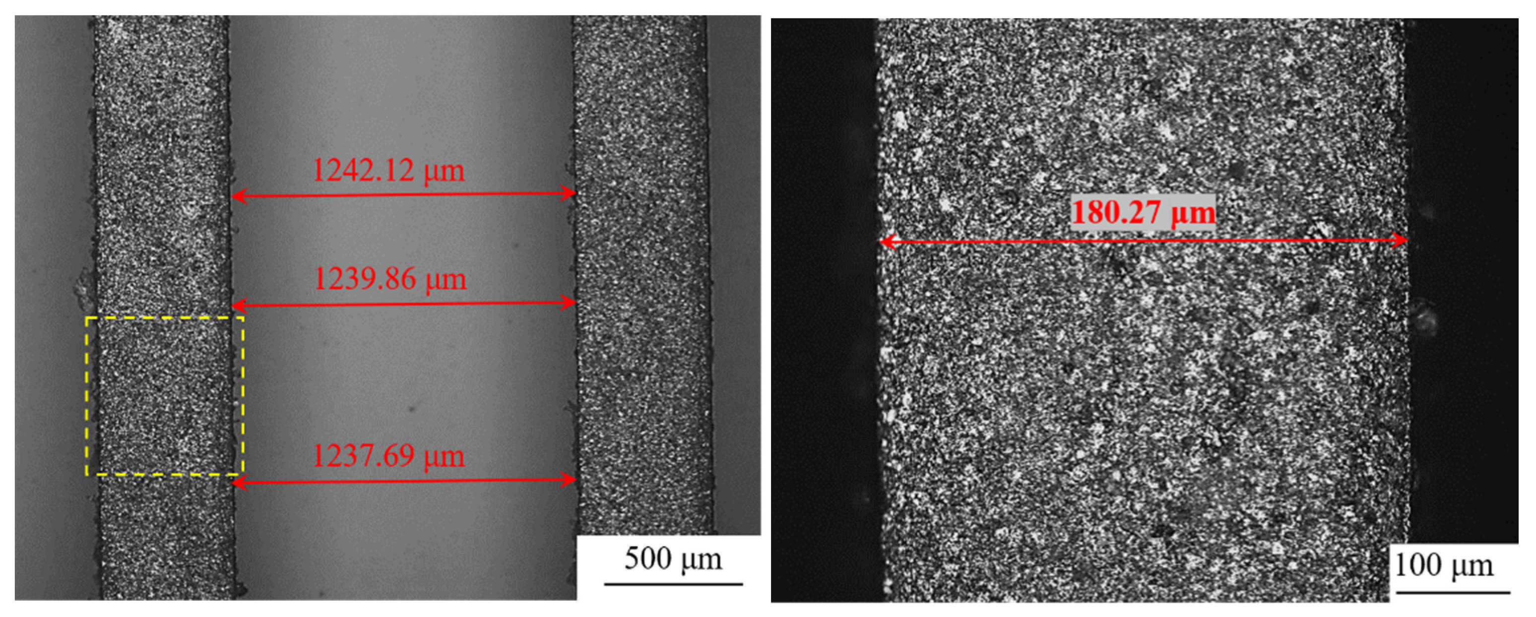
Metal waveguide components (with a three-dimensional distributed waveguide network, including receiving signal holes, local oscillator signal holes, coupling holes, etc.) are an important part of integrated heterodyne array receivers in the sub-millimeter wave band of radio telescopes. In the past, discrete waveguide components were connected by pin positioning screws to join them together, making it difficult to achieve large-scale pixels. The next-generation of array receivers with hundred-beam scale pixels must be integrated and modular. The Purple Mountain Observatory of China has proposed a 3D waveguide network with vertically distributed receiving signal holes. The 3D waveguide network must be formed as a whole, and the structure must be very compact [1]. The key to realizing this array pattern is high-precision 3D waveguide network manufacturing. Therefore, the integral forming of three-dimensional metal waveguide components is a key link in the preparation of next-generation radio telescopes [2]. A schematic diagram of the 3D metal waveguide network is shown in Figure 1. The machining accuracy of the 3D waveguide network coupling channel is controlled within 0.01 mm. The current high-speed milling technology in traditional ultrasonic additive manufacturing cannot process such coarse holes [3,4,5,6,7]. However, micro electrical discharge machining (micro-EDM) technology ensures the shape accuracy, dimensional accuracy, and surface quality of the micron-level 3D waveguide network and can form sharp corners inside the component [8]. Figure 2 shows the shape and size of the straight groove for the micro-EDM. It can be seen that the processed straight groove has a good size consistency, the error is controlled at approximately 5 μm, and the surface roughness reaches 0.6 μmRa. The new ultrasonic additive manufacturing technology integrating ultrasonic welding and micro-EDM provides a new method for the overall preparation of waveguide elements.
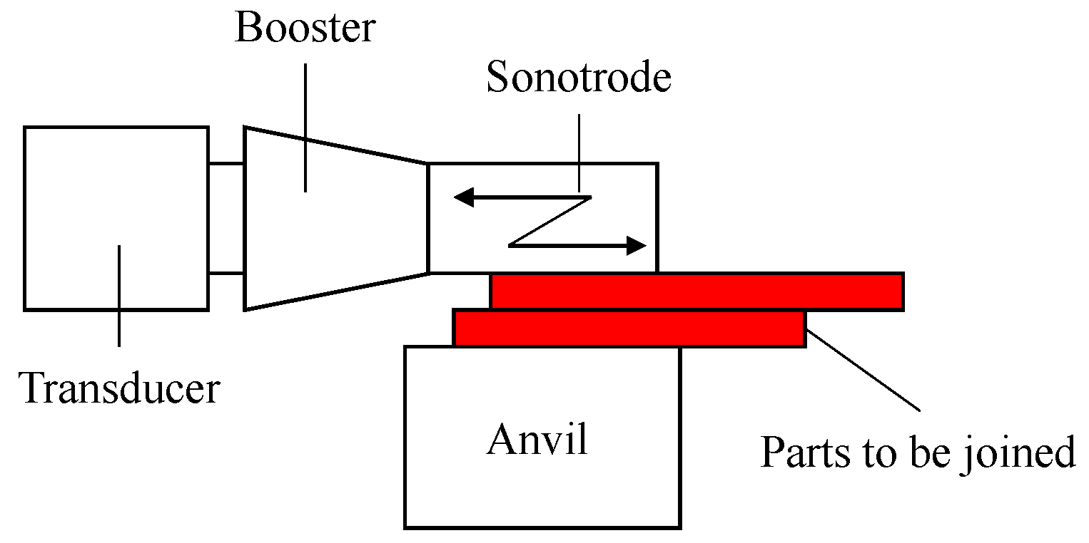
The waveguide network is usually made of metallic materials (copper, aluminum, etc.). Considering that the receiver will work at extremely low temperatures (as low as 4 K), the thermal conductivity of aluminum alloys will deteriorate at low temperatures. Therefore, Electrolytic Tough Pitch copper (Cu-ETP) is used as the research material. The effective connection of the Cu-ETP sheet is the key process for realizing the application of this technology. Ultrasonic welding technology only needs 25–50% of the melting point of the metal to realize the metallurgical connection between metal layers through ultrasonic friction, avoiding the liquid–solid phase transition, residual stress, dimensional changes and metallurgical incompatibility. The technical principle is shown in Figure 3. The vibration direction is different from that of plastic ultrasonic welding. Longitudinal vibration with pressure causes the metal sheet (the thickness is generally 0.3 mm) to achieve metallurgical bonding [9,10,11,12,13,14]. Fujii, H.T. et al. [15] studied the formation mechanism and joint failure mode of ultrasonic welding. The results show that metal bonding is the main connection mechanism of Al−Al, and physical bonding caused by friction is the main connection mechanism of the Cu−Cu or Al−Cu interface. Joint failure is a mixed failure mode of weld interface peeling and joint tearing. Nambu, S. et al. [16] found that high-frequency tangential motion during the ultrasonic welding process caused the metal interface to form nanoparticles. Under the action of the welding pressure, the nanoparticles are compacted to form a bonding interface, which is formed by mixing two specimen components. Sriraman, M.R. et al. [17] realized the high-power ultrasonic additive manufacturing of copper foil with a thickness of 150 μm at room temperature. The results show that copper involves significant material softening and plastic flow in the ultrasonic additive process. The initial grains of copper foil (25 μm in size) transform into fine dynamic recrystallized grains (0.3–10 μm in size) at the weld interface; this phenomenon is believed to be metallurgical bonding caused by a grain boundary migration. Xie, J. et al. [18] studied the recrystallization behavior of aluminum alloy ultrasonic welds by comparing the microstructure and texture of the base material and the welded specimen. The results showed that dynamic recovery (DRV) makes the weld form a layered structure with {111} and rotating cube {001} shear textures. Dynamic recrystallization (DRX) causes the weld to form uneven fine/ultrafine equiaxed grains, and the weld area has a sharp recrystallized structure {311}. We systematically explored the DRV and DRX mechanisms that control the evolution of the microstructure during the ultrasonic welding process. Fujii, H.T. et al. [19] studied the microstructure and mechanical properties of aluminum alloy/stainless steel ultrasonic welded joints. The results show that with an increasing welding energy, the fracture mode of the lap joints changes from interface peeling to base metal fracture during tension. During the welding process, the weld produces a high strain rate shear deformation and temperature rise. Through the recrystallization of aluminum alloy, the microstructure of the weld is composed of fine grains and equiaxed grains. Haddadi, F. et al. [20] used electron backscattered diffraction (EBSD) technology to study the dynamic recrystallization and grain growth of the weld during the ultrasonic welding of an aluminum alloy. The results show that high-power ultrasonic welding causes large-scale plastic deformation in the welded area. The welding seam temperature increased to 440 °C within a short welding time of 100 ms, and an ultrafine grain structure was observed at the welding interface. With an increasing welding time, the texture changed from an initially cube-dominated texture, to one where the typical β-fiber brass component prevailed.
Due to the interaction of complex factors in the ultrasonic welding process, the detailed evolution of the recrystallization behavior of the weld interface is still unclear. Moreover, the current research focuses on understanding the recrystallization behavior of metals away from the interface, and the two main bonding mechanisms on the interface are not well understood. In addition, previous work was limited to aluminum alloys, which led to insufficient research on the ultrasonic welding of copper for waveguides. In this paper, the mechanical properties (tensile load, peeling load) and the microstructure (metallography, EBSD) of welded joints are studied to evaluate the welding quality of welded joints with various process parameters, in order to study the connection mechanism of ultrasonic welding and to obtain the optimal welding parameters. EBSD technology is used to analyze the grain changes, grain boundary type changes, texture changes, etc., during the recrystallization process of the copper welding interface. ABAQUS finite element software is used to simulate the temperature field of the ultrasonic welding process of copper, and the temperature field is used to judge whether the weld temperature reaches the recrystallization temperature. The systematic exploration of this work is helpful at explaining the connection mechanism of ultrasonic welding and has important guiding significance for the control of the weld’s microstructure. The research results will provide guidance for the design process of manufacturing 3D metal waveguide devices using new ultrasonic additive manufacturing technology.

2. Experimental and Finite Element Model

2.1. Experimental Materials and Methods

In this paper, Cu-ETP was used for the welding experiment of lap joints. The specimen size was 100 mm × 20 mm × 0.3 mm, and the overlap amount was 30 mm. The model for the ultrasonic welding equipment used in the test was NC-2020A (system power P = 50~2000 W, system working force F = 460~1400 N, welding time t = 0~104 ms, welding spot area 15 × 6 mm2, ultrasonic vibration frequency f = 20 kHz). To evaluate the relationship between the ultrasonic welding process parameters and the predicted response values (welded joint tensile and shear load), the experiment adopted an orthogonal experimental design and conducted a range analysis to determine the optimal process parameters combination [21,22].
The factor level codes used in the ultrasonic welding experiment are shown in Table 1. Among them, “0” is the center point, “−” is the lower level, and “+” is the upper level.
Before welding, 320#SiC sandpaper was used to remove the surface oxide of the base metal, and acetone was finally used to completely degrade the surface oxide. The weld cross-section specimens were prepared by wire cutting. The corrosive agent FeCl3:HCl:H2O = 3 g:10 mL:100 mL was used to corrode the weld, and the corrosion time was 3–5 s. An Axio Imager A1m optical microscope was used to observe the metallographic structure of the joint. The evolution of the microtexture of the joint was analyzed by EBSD (Oxford) technology. During the test, the specimen tilt angle was 70°, the working distance was approximately 20 mm, and the acceleration voltage was 20 kV. The test data were analyzed using Aztec and Channel 5 software. A WDW3050 universal testing machine (Jinan Time Shijin Testing Machine Co., Ltd., Jinan, Shandong Province, China) was used to test the tensile load and peel load of the specimen, and the loading speeds were 3 and 15 mm/min, respectively. HVS-1000 micro Vickers hardness tester (Jiangxi Huake Precision Instrument Co., Ltd., Nanchang, Jiangxi Province, China) was used to measure the microhardness of the joint, the load was 0.025 kg, and the pressure holding time was 10 s.
To avoid systematic errors, a random ultrasonic welding experimental design is performed. The process parameters and response results are shown in Table 2.

2.2. Finite Element Model

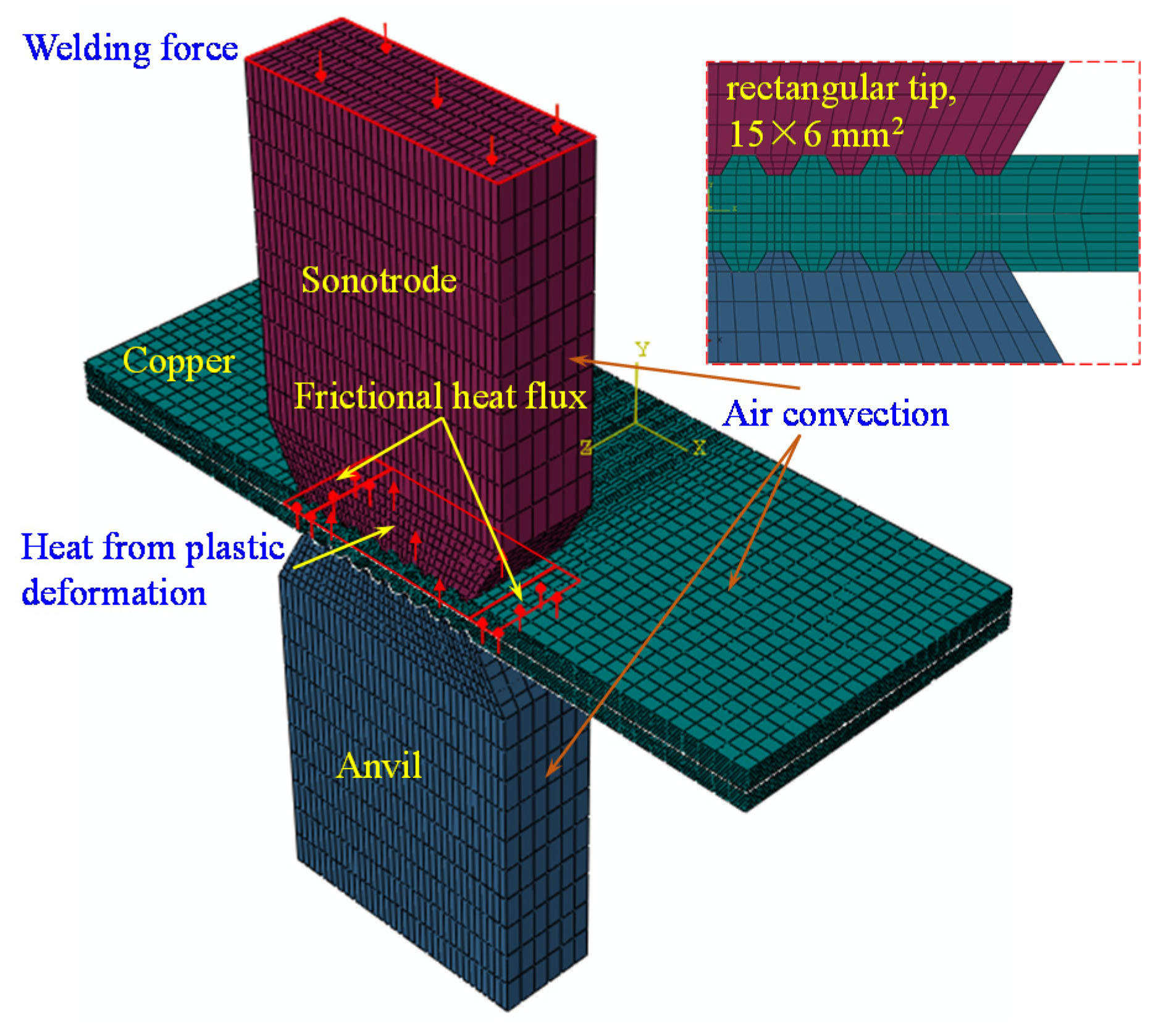
Due to the symmetry of the welded structure geometry, the boundary constraints and the load in the longitudinal plane, the finite element model was simplified based on symmetry to reduce the amount of calculation. It was assumed that there was no gap and no relative sliding on the contact surface of the sonotrode, Cu-ETP and anvil. The room temperature was 20 °C, and the sonotrode area was equal to the plastic deformation zone ADZ. ABAQUS finite element software was used to establish the ultrasonic welding model, as shown in Figure 4. The physical property parameters of the sonotrode, anvil and Cu-ETP are shown in Table 3 and Table 4 [23].
The heat source of ultrasonic welding mainly comes from the heat generated by the plastic deformation of the workpiece and the interface friction [24]. The heat flow generated due to plastic deformation was applied to the plastic deformation zone ADZ below the sonotrode. The heat flow generated by the ultrasonic vibration friction of the welding interface was applied to the interface friction area AFR near the sonotrode. The heat flow equation is calculated as follows:
The heat flow equation is generated by plastic deformation.
Q w = p T O T A L A D Z = F w ( T , F N , t ) V a v g A D Z
where
F w = ( T , F N , t ) = [ Y ( T ) 2 ] 2 ( F N / A D Z 2 ) A w ( t )
V a v g = 4 ε 0 f w
where PTOTAL is the welding power; ADZ is the plastic deformation area; Fw (T, FN, t) is the welding force [25]; Vavg is the ultrasonic welding average speed; Y(T) is the workpiece yield strength; FN is the welding static pressure; Aw(t) is the welding area; ε0 is the ultrasonic amplitude; and fw is the vibration frequency.
In a short welding time, the interface only produces a small area of mechanical interlocking, and the connection area is much smaller than the end face of the sonotrode. The welding area can be approximated as:
A w ( t ) = 1.6 ( 1 e k t / s e c ) · 10 5 · m 2   ( k   is   a   constant )
The heat flow equation generated by interfacial friction:
Q F R = P F R A F R = F F R V a v g A F R
F F R = μ F N
Q F R = 4 μ F N ε 0 f w A F R
where PFR is the frictional heat generation power; AFR is the interface friction area; FFR is the friction force; and μ is the friction coefficient.

3. Results and Discussion

3.1. Effect of the Process Parameters on the Response Value

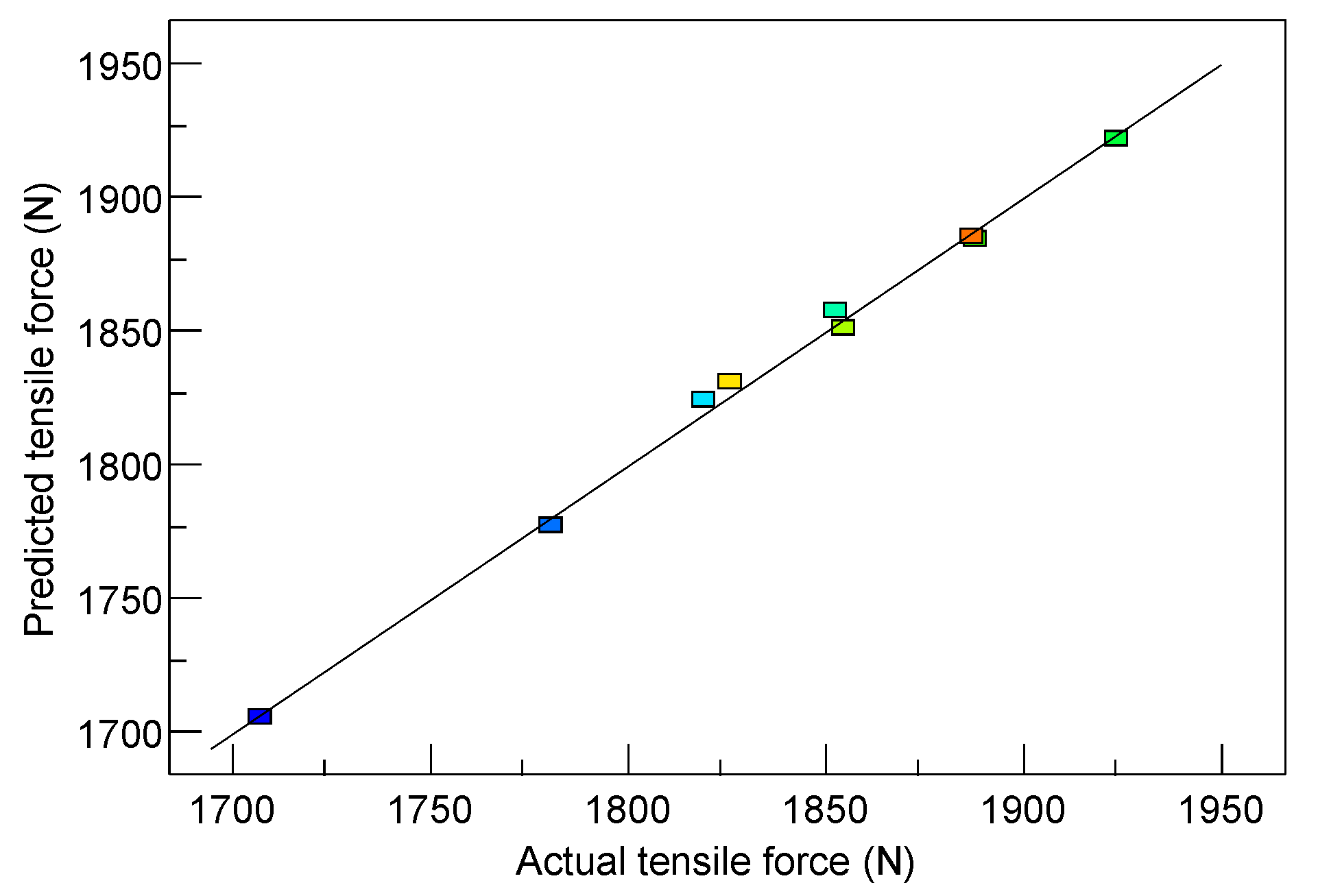
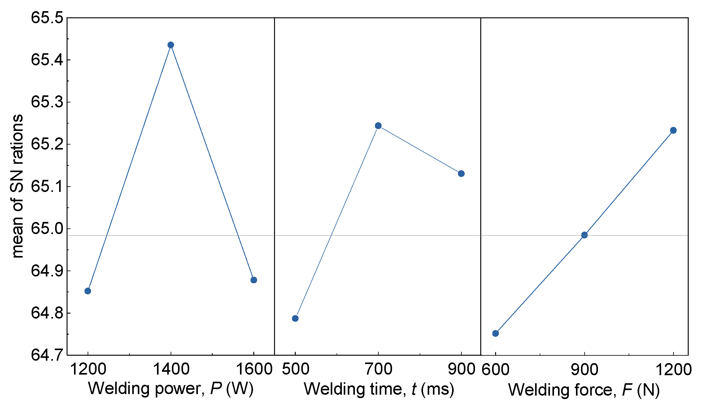
From the results of the variance analysis in Table 5, it can be seen that R2 > 90%, and the probability ∆Prob > ∆F is less than 0.05, indicating that the model can simulate the real process. Figure 5 is a scatter diagram of the predicted response and its actual values, indicating that the regression model is not unfit. From the comparison of ∆Prob > ∆F values, it is determined that the degree of influence of each parameter on the tensile load is P > t > F. This paper adopts general optimization standards for copper ultrasonic welding and sets the target as the maximum ultimate tensile strength. Additionally, the welding process parameters are kept within the design space domain. From the main effect diagram of the signal to noise (SN) ratios in Figure 6, the optimal process parameters combination can be predicted as P = 1400 w, t = 700 ms, and F = 1200 N.
The influence of various factors on the response value of Cu-ETP ultrasonic welded joints includes the welding energy P, welding time t and welding force F, and the influence of the various process parameters on joint quality is not simply superimposed but instead interactive. Therefore, the influence of the welding heat input (P × t) and welding force F on joint quality is analyzed below.
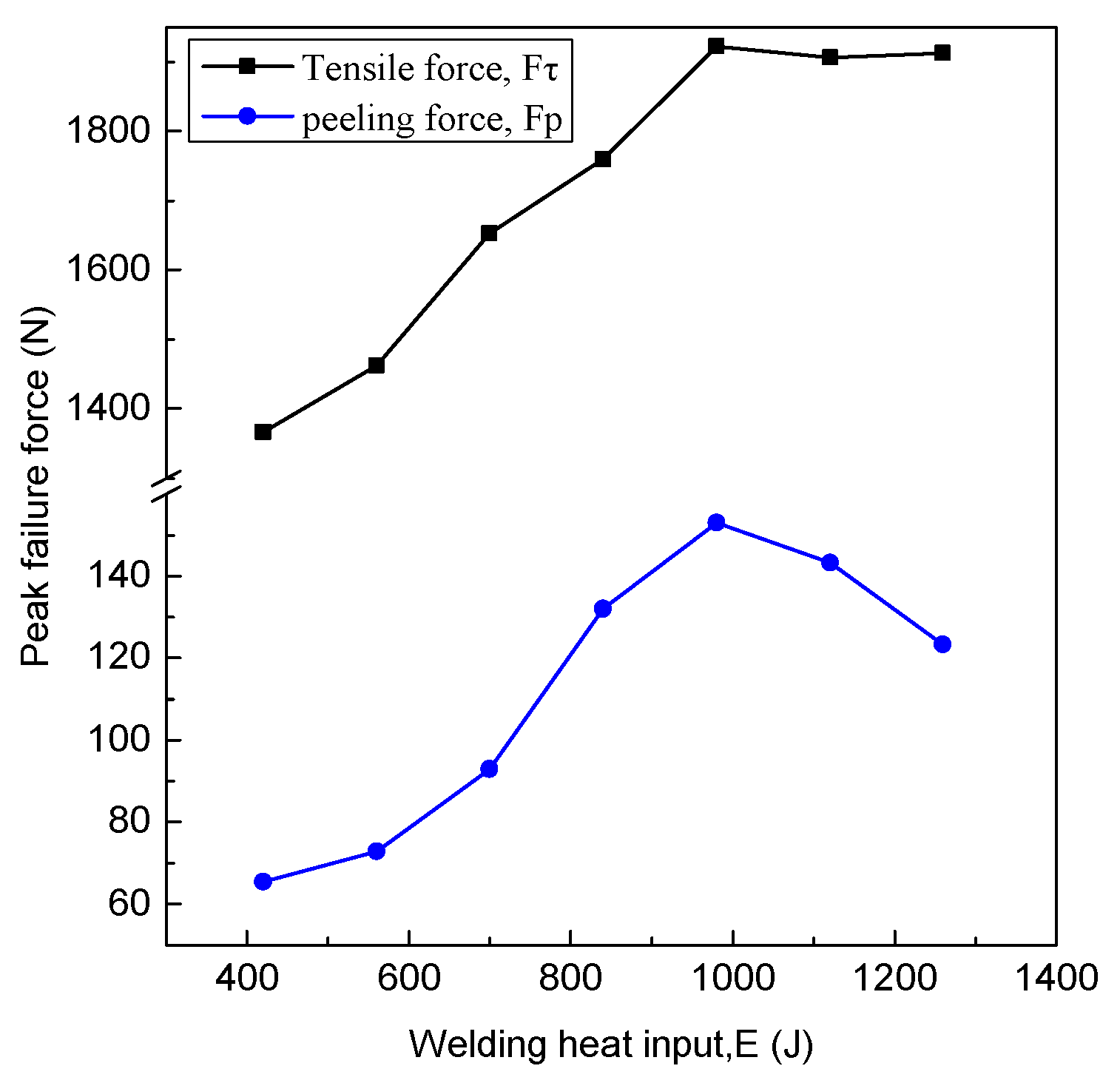
Figure 7 shows the metallographic structure of Cu-ETP welds at different welding heat inputs when the welding force is 1200 N. At a low welding heat input, the quality of the joint is only determined by the welding force and the ultrasonic vibration to achieve mechanical fitting of the local contact surface. With an increase in the welding heat input, the welding workpiece appears softened, and a small amount of plastic deformation makes the interface tightly connected. When the heat input is 700 ms × 1400 W, the connection line is not obvious, which also shows that the joint has the best mechanical performance. With a further increase in heat input, the welding workpiece softens, and the plastic deformation intensifies, resulting in a stress concentration in the local connection area and a decrease in the mechanical properties. The corresponding tensile load and peeling load curves are shown in Figure 8.
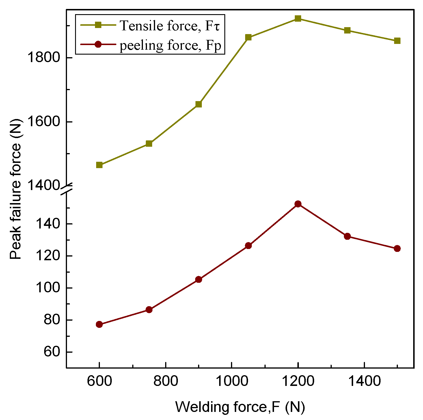
Figure 9 shows the metallographic structure of Cu-ETP welds at different welding forces when the welding heat input is 500 ms × 1400 w. It can be seen that due to the low static friction of the interface under a low welding force, false solder appears on the bonding surface. When the welding force is 1200 N, the grains near the weld are significantly refined, and the joint is well bonded. Excessive welding force causes severe deformation of the weld and microcracks in some areas, which reduces the quality of the joint connection. The corresponding tensile load and peel load curves are shown in Figure 10.
The ultrasonic welding process is complicated, involving not only mechanical interlocking but also interatomic diffusion and dynamic recrystallization of crystal grains [26]. In the early stage of Cu-ETP ultrasonic welding, the welds were not directly bonded but instead partially mechanically interlocked. Due to the low welding heat input or low welding force, the welding energy between the interfaces is insufficient. Under the action of an external force, the connecting surfaces squeeze and cause friction on one another to form a mechanical interlock. Mechanical interlocks are usually jagged. This type of interlocking is only macroscopic mechanical interlocking, and it is easy to detach under the action of an external force, so the tensile load and peeling load of this joint are relatively low. As the welding energy or welding force increase, the mechanical interlock will gradually decrease. This shows that mechanical interlocking is not the main connection mechanism of copper ultrasonic welding.
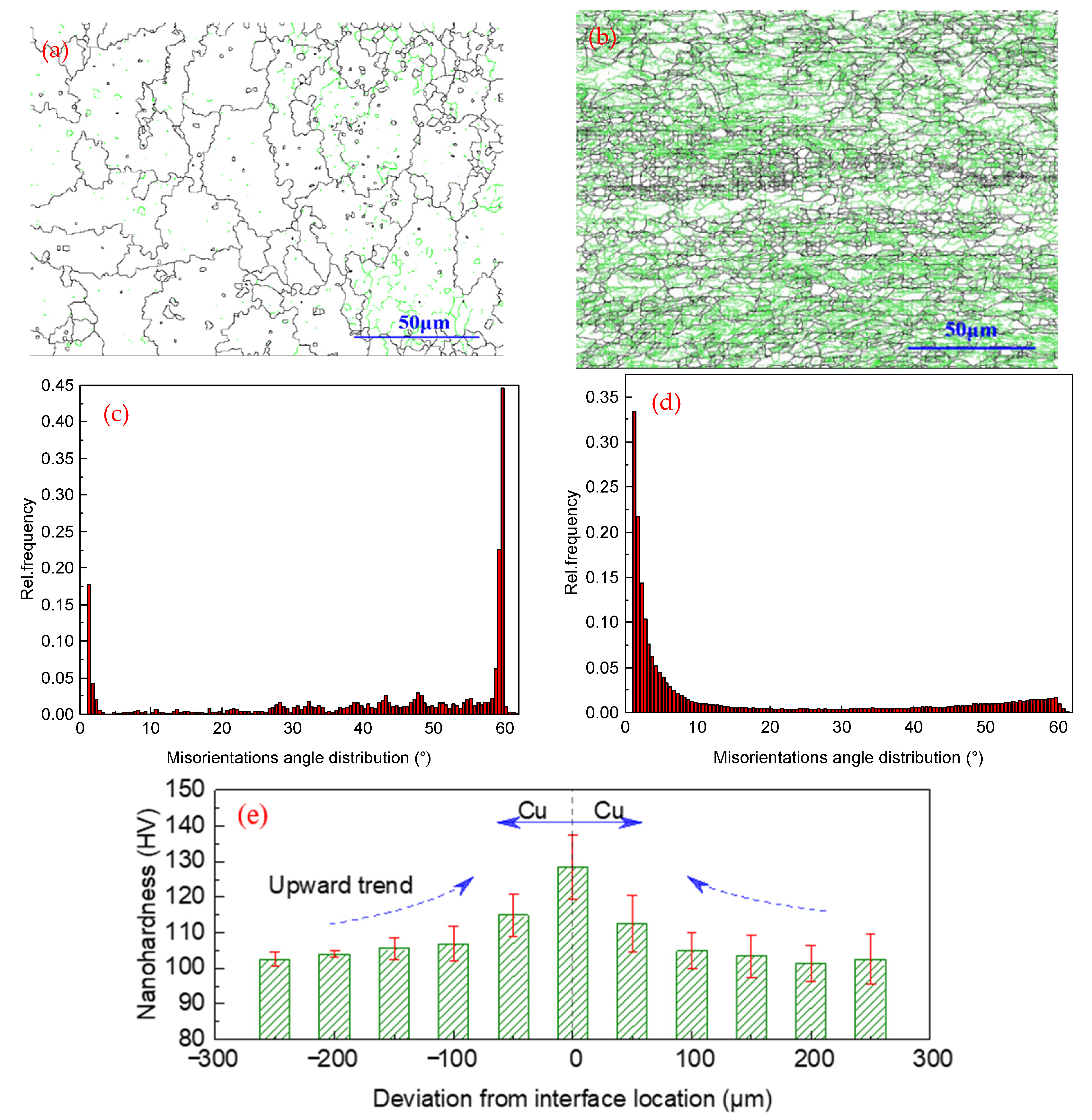
Under the action of static pressure and high-frequency vibration, the interface temperature of the joint increases rapidly. When the energy acquired by the atom is greater than its activation energy for diffusion, the atom diffuses, and the metal atoms interact to form a bond. Metal bonding enhances the mechanical properties of welded joints. This shows that metal bonding plays a key role in the ultrasonic welding of Cu-ETP. The grain boundary misorientation angle is less than 5° as indicated by the green line in Figure 11, and the grain boundary misorientation angle is greater than 5°, as marked by the black line in Figure 11. Figure 11a,b shows that the quantity of small-angle grain boundaries increases significantly after welding. The fraction of grain boundary misorientation distribution in Figure 11c,d also shows this trend. These results lie in the plastic deformation of the welded joint during the welding process, which leads to an increase in the dislocation density. The welding process increases the temperature of the substrate, which leads to the climbing of ductile dislocations and the cross-slip of screw dislocations. The dislocations gradually evolve into multilateral structures and then develop into small-angle grain boundaries. From the grain distribution of Cu-ETP welded joints with the optimal process, it shows that there are a large number of coarse columnar grains far away from the weld area. Due to recrystallization, a large number of small equiaxed grains with a diameter of a few microns are generated in the area adjacent to the weld. These newly generated fine equiaxed grains increase the number of grain boundaries, hinder the movement of dislocations and improve the strength and plasticity of the material. Figure 11e shows the distribution of the micro Vickers hardness of the joint. It can be seen that the microhardness of the connecting interface area is higher than that of the base material (~91 HV). These results further indicate that severe plastic deformation, grain refinement and dislocation multiplication occurred in the interface zone.

3.2. Analysis of Interface Recrystallization Behavior

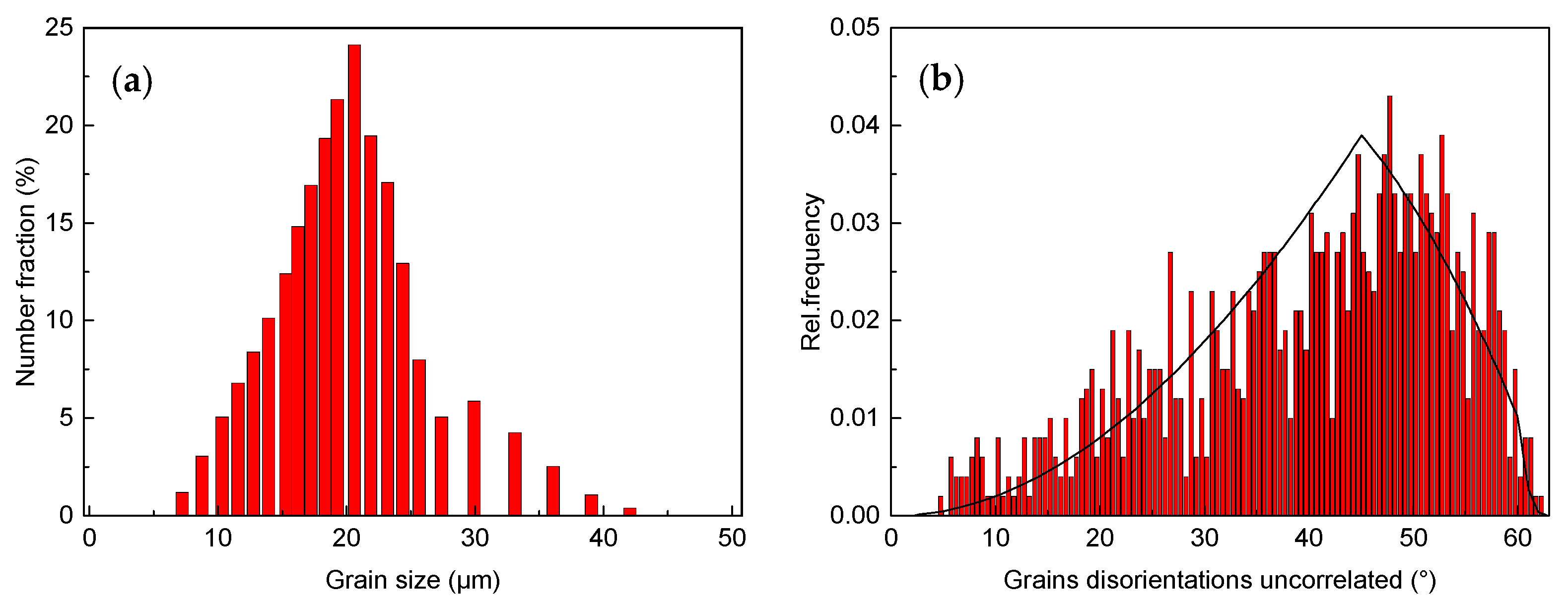
The microstructure of Cu-ETP mainly includes coarse grains with HAGBs (phase difference α > 15°), with a large number of annealing twins. The base metal structure is unevenly distributed, and the grain size is 10~30 μm (Figure 12a). The misorientation distribution of the base material grains (columnar line) is essentially consistent with the random distribution curve (black curve). This shows that the misorientation distribution of the copper base material obtained by annealing conforms to the theoretical value. In addition, these misorientations include not only the grain boundaries, but also the sub-grain boundaries inside the grains (Figure 12b).
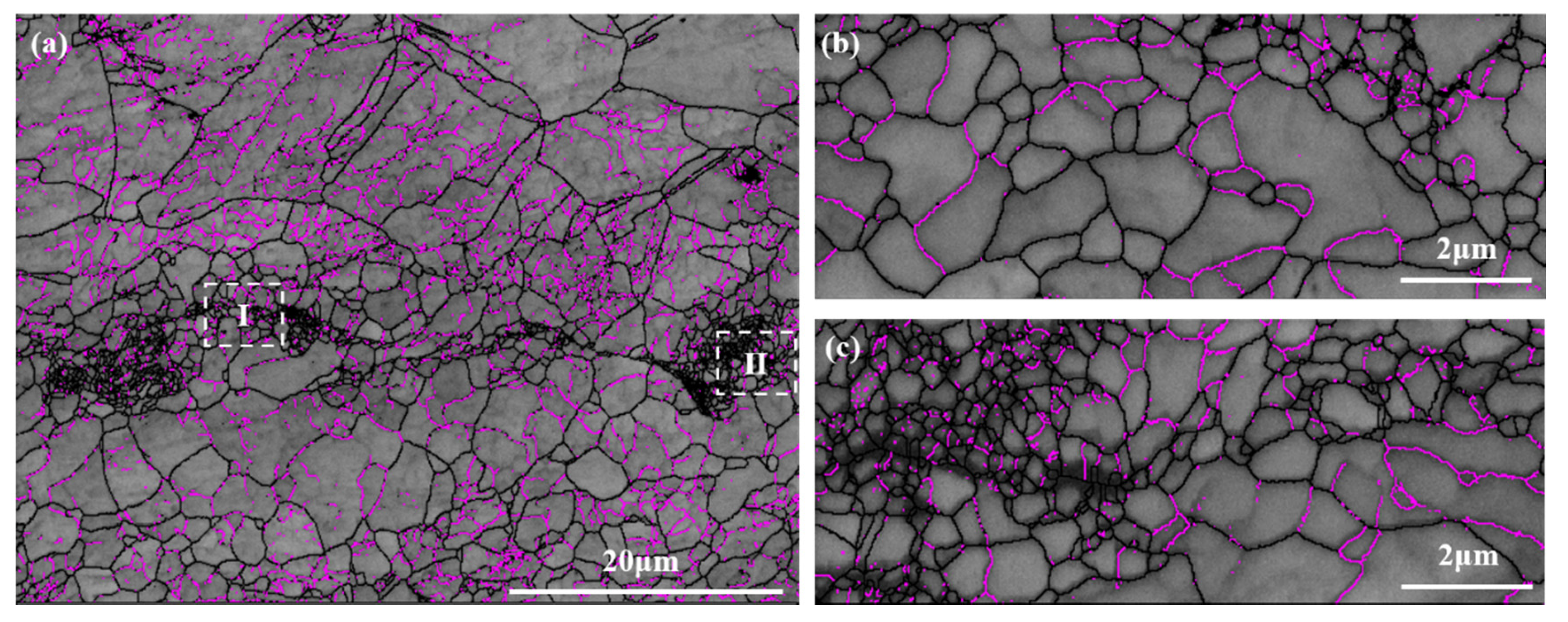
The grain boundary map of the copper ultrasonic welded joint is shown in Figure 13. The purple line represents the high-angle grain boundary. It can be seen that there are no visible defects in the weld, such as cracks or virtual welds. The area far away from the welding interface is composed of coarse deformed grains and a large number of low-angle grain boundaries (LAGBs; phase difference α < 15°). These LAGBs are generally accompanied by the generation of subcrystals and dislocations. The gradual disappearance of copper twins is due to the welding pressure and ultrasonic vibration that promote the deformation and movement of the twins, thereby forming coarse deformed grains. The welding interface area is mainly composed of uneven regenerated small equiaxed grains, which are gathered together in large numbers with a minimum size of 0.5 μm. This is because the fine grains regenerated during the ultrasonic welding process aggregate under the action of plastic flow. When the temperature reaches the recrystallization temperature, the original crystal defects (dislocations, grain boundaries, etc.) will re-nucleate and grow into distortion-less equiaxed crystals. Therefore, the appearance of small equiaxed crystals in the joint is an important sign of copper recrystallization during ultrasonic welding. In addition, a small number of slender layered structures are generated in the interface area, which is related to the dynamic recovery effect during the ultrasonic welding process. At the same time, a large number of HAGBs are generated, while the LAGBs are significantly reduced, which is due to the copper recrystallization temperature reached during the welding process. Some LAGBs (subcrystals) merge with adjacent subcrystals to form high-angle grain boundaries, and the other LAGBs (dislocations) are entangled and migrate to form high-angle grain boundaries due to an increase in the external pressure and activation energy.
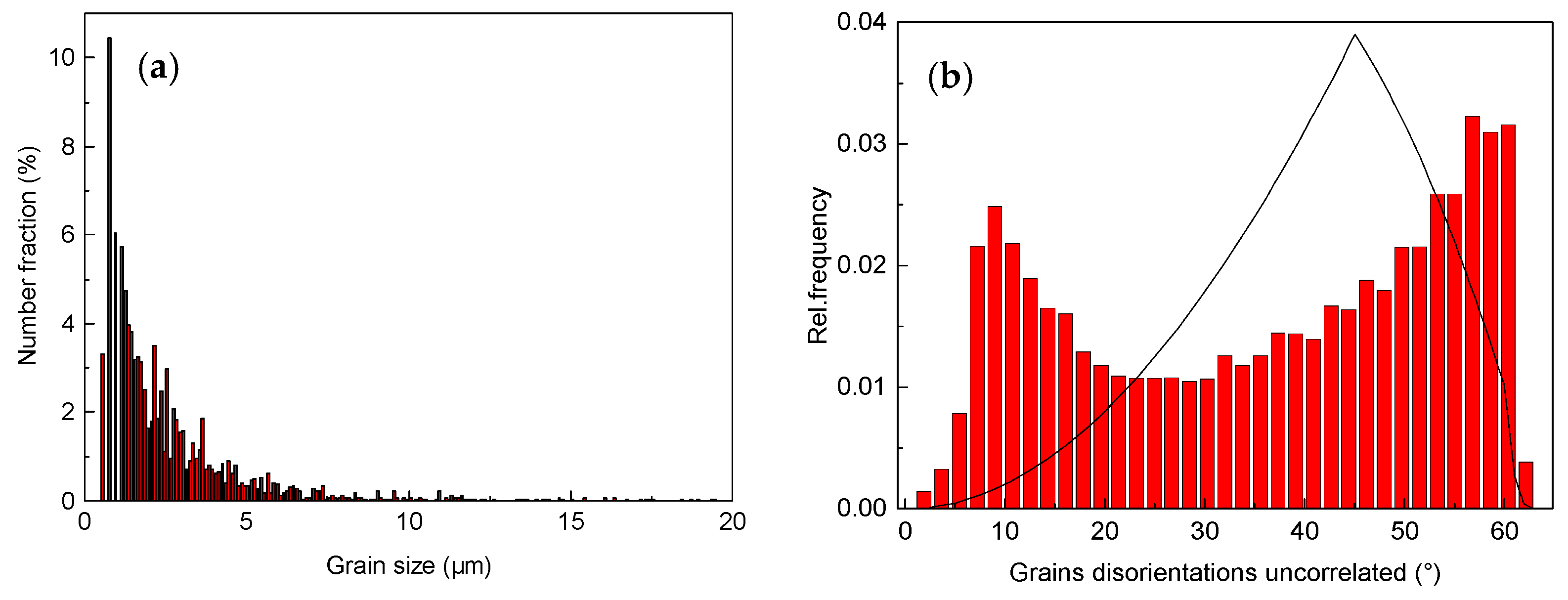
Figure 14 is a statistical graph of the grain size and misorientation of the welded joint. The grain size of copper is obviously reduced after ultrasonic welding, and the average grain size is 1~2 μm. The grain size is relatively concentrated, and most of the grain size is in the range of 1~10 μm, which shows that ultrasonic welding has the effect of grain refinement (Figure 14a). It can be seen from the misorientation statistical graph that the misorientation has changed from high to low. This shows that the small-angle grain boundaries increase after ultrasonic welding, and the large-angle grain boundaries decrease, which corresponds to Figure 13 (Figure 14b).
There is no strong oriented texture in the copper base material, mainly brass texture {112}<111>, (<001>‖ND) and a cubic texture {001}<100>, (<001>‖ND). Figure 15 shows the distribution of the EBSD inverse pole figure (IPF) of the Cu-ETP ultrasonic welding interface microstructure and the crystal plane pole figure (PF) of the microstructure at {100}, {101} and {001}. It can be seen that the welds mainly have shear textures {111}<143>, {111}<110> (blue position) and {221}<122> (purple position), and parts of the {001}<130>, {001 }<230> and {114}<131> textures, etc. Among them, there are many regenerated fine cubic textures {100}<001> (red position) and shear textures {111}<110> at the welding interface. The evolution of the interface texture is related to the DRV and DRX mechanisms during ultrasonic welding.
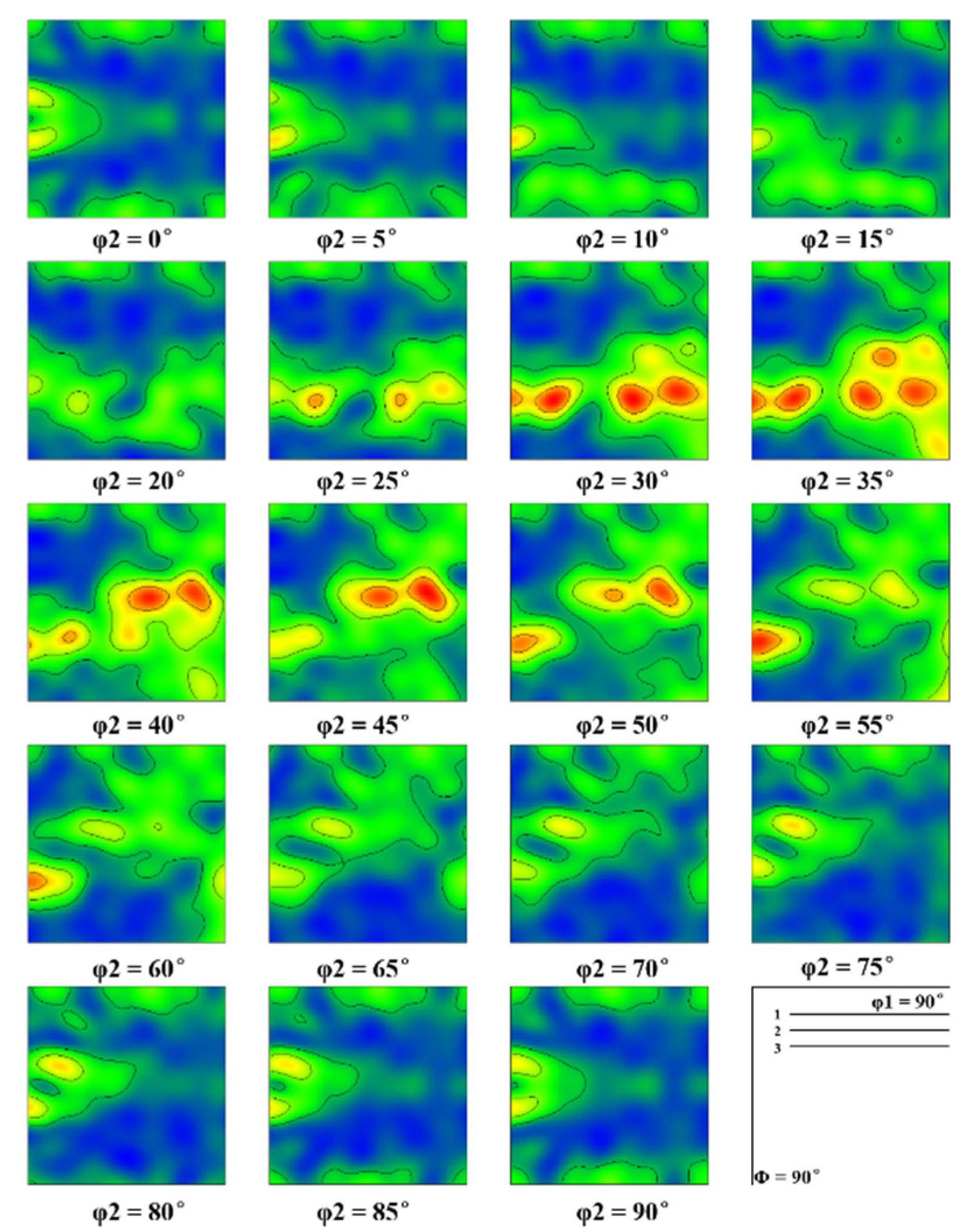
The orientation distribution function (ODF) diagram can be used to quantitatively and accurately analyze the spatial distribution of the grain orientation in the texture material to further characterize the microstructure of the weld (Figure 16). The ODF map was measured to obtain the Euler angle, and the Euler angle was used to calculate the micro-textures in different regions. It can be seen that there are {001} <100> cubic textures, {001} <110> rotating cube textures and {111} <143>, {221} <122> deformation textures in the Cu-ETP welds. This cubic texture is not the cubic texture of the base material but is instead produced during the recrystallization process with ultrasonic welding. The cubic texture in the base metal becomes the core of recrystallization under the action of ultrasonic excitation and welding pressure and finally grows into a new recrystallized cubic texture. The cubic texture is also one of the main recrystallization textures of face-centered cubic crystals. The deformation texture is produced by the plastic deformation of the joint during the welding process. The reason is that the base material grains are produced via plastic deformation, and the newly formed recrystallized grains are deformed during the ultrasonic welding process.

3.3. Numerical Simulation Results and Analysis

The recrystallization behavior of metallic materials occurs within a certain temperature range. The recrystallization temperature is not a fixed physical constant but is instead affected by many factors. The most significant factor is the degree of metal deformation. As the degree of deformation increases, the more energy stored inside the material, the greater the driving force for recrystallization, which reduces the recrystallization temperature. The grain size of the base material also has a greater influence on the recrystallization temperature. The smaller the grain size is, the lower the recrystallization temperature. This is because most of the recrystallization nuclei are located at grain boundaries and dislocations. The finer the grains, the more grain boundaries there are, and the easier recrystallization and nucleation are. In addition, there are other factors that affect the recrystallization temperature, such as material solute atoms and second-phase particles. Generally, in pure metals with a large degree of deformation, the recrystallization temperature is approximately (0.35–0.4) Tm (the melting point of pure metals). The melting point of copper is 1083°C, so the recrystallization temperature of copper is approximately 379.05–433.2 °C.
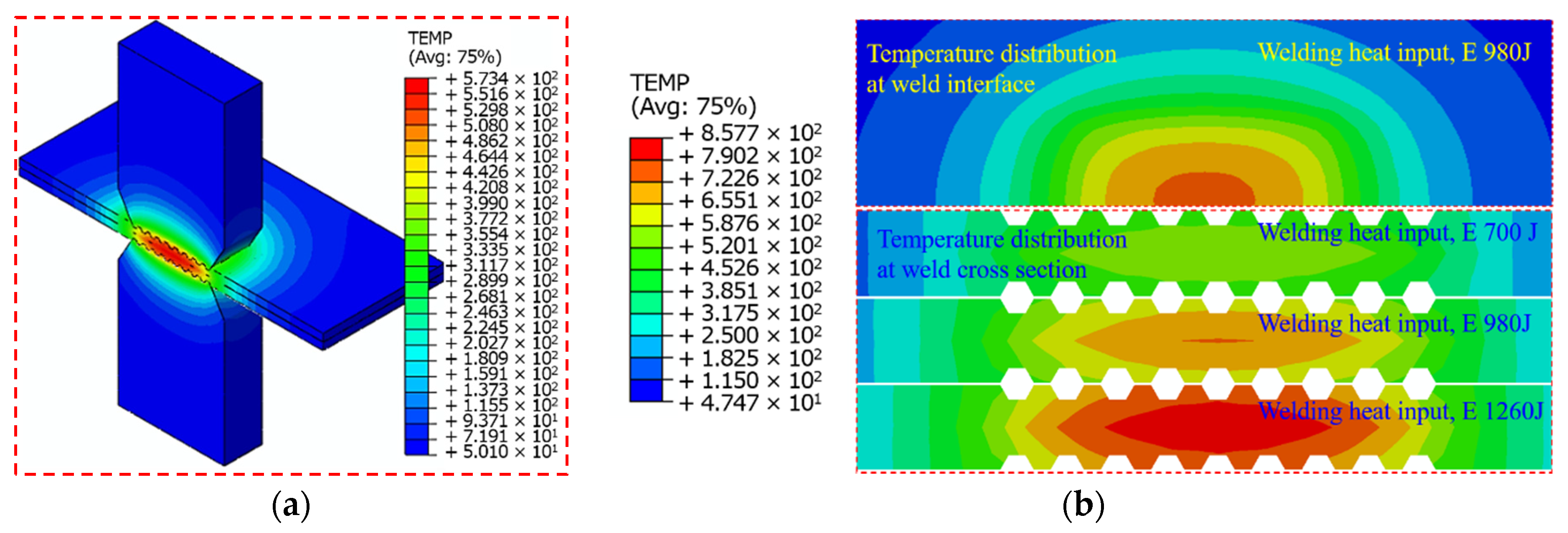
Figure 17 shows the simulation results of the temperature field with different welding heat inputs at a welding force of 1200 N. As the welding heat input increases, the temperature at the center of the welding interface also increases. The center point temperatures are 573, 723 and 858 °C, while the melting point of copper is 1083 °C. The temperature below the melting point indicates that ultrasonic welding is a solid phase connection technology. The maximum temperatures reached 52.9%, 66.8% and 79.2% of the melting point of copper, respectively. Within the range of 30% to 80%, the simulation results are reasonable. In addition, it can be seen from the temperature field that the area near the weld is a high-temperature area, and the central area has the highest temperature. The temperature of the contact area between the sonotrode and the copper is significantly lower. When the welding heat input is 980 J, the temperature in the center area rises sharply to 400 °C within 100 ms of the welding time. It can be seen that the energy conversion is very fast in the ultrasonic welding process. Then, the temperature slowly rises linearly with time, and the final temperature reaches 723 °C. From the Cu-ETP recrystallization temperature range combined with the simulation results, it can be seen that the temperature in the vicinity of the welding interface has reached the recrystallization temperature.

3.4. Analysis of DRV and DRX

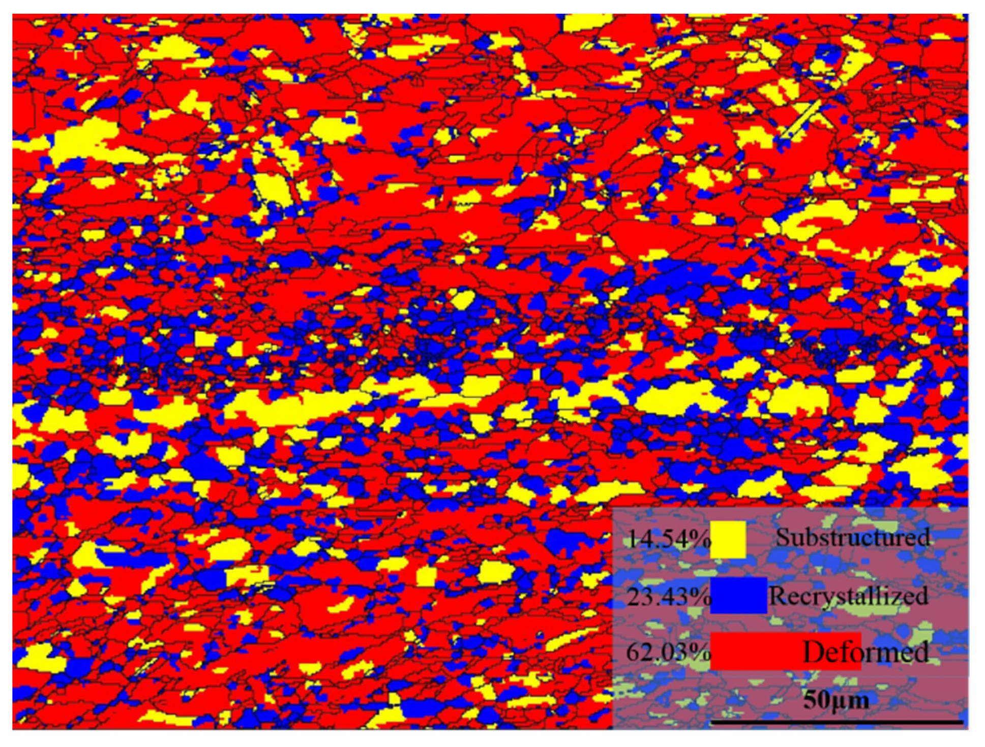
For the analysis of the microstructure, the texture and numerical calculation results show that the Cu-ETP welding interface produces strong shear plastic deformation and reaches the recrystallization temperature under the combined action of high frequency excitation and welding pressure during the ultrasonic welding process. The microstructure changes and connection mechanisms are dominated by DRV and DRX [27,28,29]. Figure 18 is a statistical graph of the EBSD recrystallization fraction of the welded joint. Blue is the recrystallized area (23.43%), yellow is the sub-structured area (14.54), and red is the deformed grain area (62.03%). It can be seen that the recrystallized areas are mostly located near the welding interface, while the subcrystals are mostly near the recrystallized grains and the deformed grains are mostly far away from the welding interface. The research results show that DRV and DRX formed a slender layered structure and ultrafine equiaxed grains, respectively, during the ultrasonic welding process.
Due to the combined effect of the welding pressure and ultrasonic vibration on the workpiece, the copper grains are deformed. With an increasing strain, the dislocations continue to multiply, and the dislocation density continues to increase. They gradually entangle one another or form a cellular substructure. These defects return to the undistorted state before being deformed, and the temperature rises continuously during the ultrasonic welding process, which provides an exciting energy for the recovery process. When the internal temperature of the crystal is high enough and the energy is large enough, the dislocations will migrate, the dislocation nodes will be unpinned, and the unlike dislocations will be offset when they are in contact on the new slip surface to reduce the dislocation density. It is worth noting that there is no large-angle grain boundary migration during the recovery process. DRV-driven dislocation climbing and cross-slips will form dislocation cells or subcrystals. At the same time, a few unstable crystal grains may split and form high-orientation boundaries to separate the dislocation cell masses and form elongated, layered deformation bands. Finally, the deformation bands evolved into elongated layered particles rich in LAGBs. Unstable splitting is considered to be the initial stage of ultrafine grain formation on the bonding surface. This may also contribute to the uneven distribution of fine grains at the bonding interface.
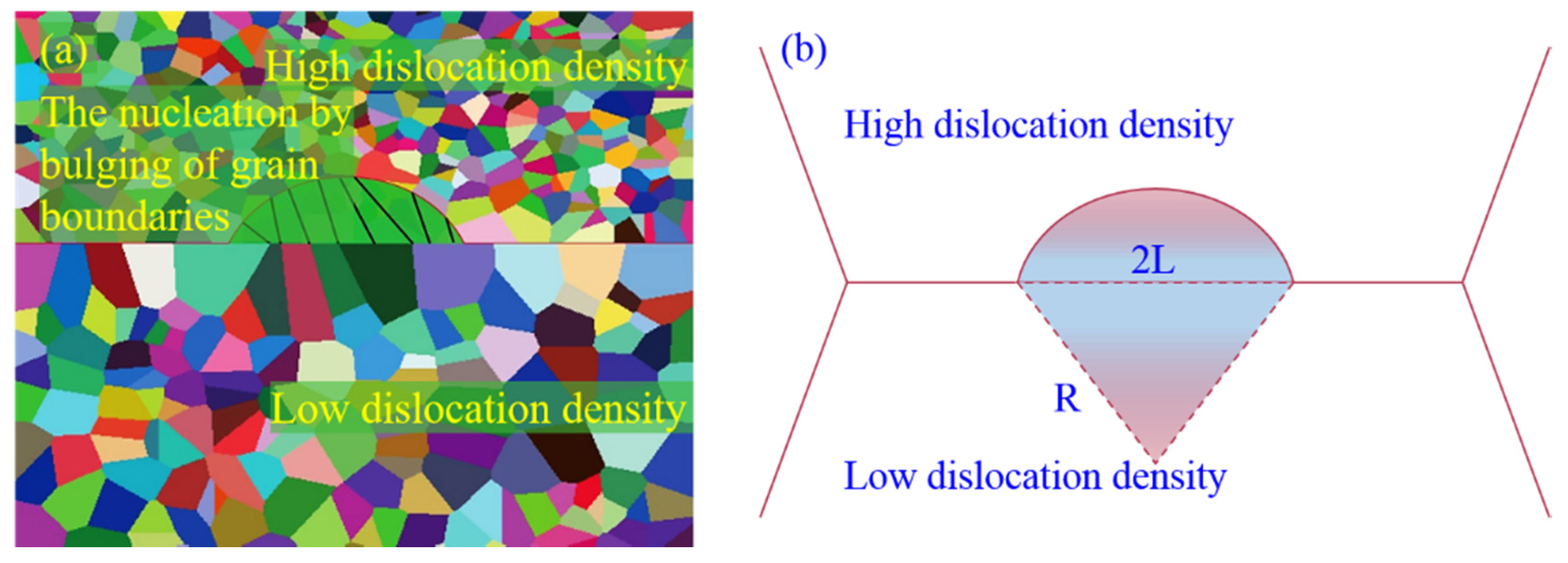
The method of dynamic recrystallization is related to the strain inside the material. When the strain is small, as shown in area I in Figure 13, discontinuous dynamic recrystallization (DDRX) mainly occurs. DDRX mainly nucleates and grows at the original grain boundary or the trigeminal node of the grain boundary. That is, the nucleation grows by arching the nucleation mode at the grain boundary. When the crystal strain is small, the dislocation density of adjacent crystal grains is different due to an uneven deformation. A grain with a large degree of deformation usually has a larger dislocation density, and a large dislocation density will increase the number of subcrystals formed inside the grain and reduce the size [18,30]. To reduce the free energy of the system, part of the subcrystals in the crystal grains with low dislocation density will migrate to the crystal grains with a high dislocation density through the adjacent grain boundary arching method and then merge the subcrystals to recrystallize the nucleus without distortion (Figure 19a). Figure 19b shows the DDRX nucleation model of grain boundary removal. The equation is:
  Δ E 2 γ L
where γ is the surface energy of copper (approximately 1.81 J·m−2); and L is the chord corresponding to the bulging arc (approximately 5 μm). This shows that the DDRX nucleation energy of copper is 7.24 × 10⁵ J. Due to the combined effect of the welding pressure and ultrasonic vibration. The welding energy is much greater than this value, and the material will undergo plastic deformation. Therefore, ultrasonic welding provides the energy and strain conditions for DDRX nucleation.
Continuous dynamic recrystallization (CDRX) mainly occurs in areas with large plastic deformation (Figure 13c). Due to the high frequency friction existing in the interface area, the material in this area produces severe shear plastic deformation and obtains a higher temperature. At the same time, dislocation cells or subcrystals produced by DRV can also trigger CDRX. The process is as follows: First, the shear plastic deformation drives the sliding of dislocations within the subcrystals. To adapt to the adjacent strain incompatibility, subcrystal boundaries are combined with sliding dislocations, and the grains are refined by CDRX. Finally, the subcrystals with LAGBs become fine equiaxed CDRX grains with HAGBs through an increase in the misorientation and subgrain/grain boundary rotation. Since subcrystalline nucleation is a form of CDRX nucleation, subcrystalline grains are often accompanied by CDRX grains (Figure 18). When the metal is deformed to a large extent, the dislocations in the crystal continue to multiply, and the dislocations entangle with one another to form a cellular structure. As the temperature rises, the cell walls become flat and form subcrystals. Some of the subcrystals can merge with adjacent subcrystals to form HAGBs, which have a higher mobility and can move quickly to eliminate dislocations during movement, thereby forming a distortion-free recrystallization core. The other part of the subcrystals, due to its large misorientation, tends to migrate as the temperature rises and transforms into LAGBs before developing into recrystallization cores.

4. Conclusions

To summarize, we have demonstrated that the orthogonal test optimization method can be used to conduct ultrasonic welding tests on pure Cu with a thickness of 0.3 mm. The process parameters combination of joint welding can be evaluated and optimized by studying the joint microstructure and mechanical properties. Besides, using EBSD technology to analyze the microstructure and texture changes of the welded joints, and combining the finite element method to study the recrystallization process of copper ultrasonic welding.
(1) The micro-EDM straight groove size error is approximately 5 μm, and the surface roughness reaches 0.6 μmRa, which can form sharp corners inside the component and ensures the machining accuracy and surface quality of the micron-level 3D waveguide network.
(2) The optimal process parameters combination of Cu-ETP ultrasonic welding were obtained through experiments (P = 1400 W, t = 700 ms, F = 1200 N). The finite element calculation temperature peak value under this parameter reached 723 °C, which exceeded the recrystallization temperature of Cu-ETP from 379.05 to 433.2 °C. The quality of the welded joint is determined by the mechanical interlocking of the local contact surface at a low welding heat input. However, this interlocking is only a macroscopic mechanical fitting, and it is easy to detach under the action of an external force. When the energy acquired by the atom is greater than its activation energy for diffusion, as the welding heat input increases the atom diffuses, and the metal atoms interact to form a bond.
(3) There are LAGBs, subcrystalline grains and fine equiaxed grains in the Cu-ETP weld, and the average grain size is approximately 1–2 μm. These newly generated fine equiaxed grains increase the number of grain boundaries, hinder the movement of dislocations and improve the strength and plasticity of the material.
(4) The microstructure, texture and numerical calculation results show that Cu-ETP has DRV and DRX effects. The DRV and DRX effects make the weld form a slender layered structure and ultrafine equiaxed grains and play a leading role in microstructure changes and adhesion mechanisms. After welding, the brass texture {112}<111> and cubic texture {001}<100> are transformed into shear textures {111}<143>, {111}<110> and {221}<122>, as well as some other textures, such as {001}<130>, {001}<230>, {114}<131>, etc. In addition, there are a large number of regenerated fine cubic textures {100}<001> and shear textures {111}<110> at the welding interface.

Author Contributions

Conceived and designed the experiments, finite element simulation, performed the experiments, writing—original draft, Z.S.; funding acquisition, conceived and designed the experiments, writing—review & editing, Z.Z.; Funding acquisition, performed the experiments, Y.Z.; data analysis, writing—review & editing, H.Z.; sample fabrication, Q.X. All authors contributed to the data analysis and discussion. All authors have read and agreed to the published version of the manuscript.

Funding

This research was funded by the financial support from the National Natural Science Foundation of China (grant no. U1731118) and the Science and Technology Research Project of Jiangxi Provincial Department of Education (GJJ190918).

Institutional Review Board Statement

Not applicable.

Informed Consent Statement

Informed consent was obtained from all subjects involved in the study.

Data Availability Statement

The data presented in this study are available on request from the corresponding author.

Conflicts of Interest

The authors declare no conflict of interest.

References

  1. Shan, W.; Yang, J.; Shi, S.; Yao, Q.; Zuo, Y.; Lin, Z.; Chen, S.; Zhang, X.; Duan, W.; Cao, A.; et al. Development of Superconducting Spectroscopic Array Receiver: A Multibeam 2SB SIS Receiver for Millimeter-Wave Radio Astronomy. IEEE Trans. Terahertz Sci. Technol. 2012, 2, 593–604. [Google Scholar] [CrossRef]
  2. Groppi, C.; Kawamura, J.H. Coherent Detector Arrays for Terahertz Astrophysics Applications. IEEE Trans. Terahertz Sci. Technol. 2011, 1, 85–96. [Google Scholar] [CrossRef]
  3. Wang, Y.; Yang, Q.; Liu, X.; Liu, Y.; Liu, B.; Misra, R.D.K.; Xu, H.; Bai, P. Microstructure and mechanical properties of amorphous strip/aluminum laminated composites fabricated by ultrasonic additive consolidation. Mater. Sci. Eng. A 2019, 749, 74–78. [Google Scholar] [CrossRef]
  4. Friel, R.J.; Harris, R.A. Ultrasonic Additive Manufacturing–A Hybrid Production Process for Novel Functional Products. Procedia CIRP 2013, 6, 35–40. [Google Scholar] [CrossRef] [Green Version]
  5. Kelly, G.S.; Just, M.S.; Advani, S.; Gillespie, J.W. Energy and bond strength development during ultrasonic consolidation. J. Mater. Process. Technol. 2014, 214, 1665–1672. [Google Scholar] [CrossRef]
  6. Kelly, G.S.; Advani, S.; Gillespie, J.W.; Bogetti, T.A. A model to characterize acoustic softening during ultrasonic consolidation. J. Mater. Process. Technol. 2013, 213, 1835–1845. [Google Scholar] [CrossRef]
  7. Kelly, G.S.; Advani, S.G.; Gillespie, J.W. A model to describe stick–slip transition time during ultrasonic consolidation. Int. J. Adv. Manuf. Technol. 2015, 79, 1931–1937. [Google Scholar] [CrossRef]
  8. Zhang, L.; Tong, H.; Li, Y. Precision machining of micro tool electrodes in micro EDM for drilling array micro holes. Precis. Eng. 2015, 39, 100–106. [Google Scholar] [CrossRef]
  9. Dehoff, R.; Babu, S. Characterization of interfacial microstructures in 3003 aluminum alloy blocks fabricated by ultrasonic additive manufacturing. Acta Mater. 2010, 58, 4305–4315. [Google Scholar] [CrossRef]
  10. Sridharan, N.; Norfolk, M.; Babu, S.S. Characterization of Steel-Ta Dissimilar Metal Builds Made Using Very High Power Ultrasonic Additive Manufacturing (VHP-UAM). Met. Mater. Trans. A 2016, 47, 2517–2528. [Google Scholar] [CrossRef]
  11. Gao, S.; Wu, C.; Padhy, G.; Shi, L. Evaluation of local strain distribution in ultrasonic enhanced Al 6061-T6 friction stir weld nugget by EBSD analysis. Mater. Des. 2016, 99, 135–144. [Google Scholar] [CrossRef]
  12. Ward, A.A.; French, M.R.; Leonard, D.N.; Cordero, Z.C. Grain growth during ultrasonic welding of nanocrystalline alloys. J. Mater. Process. Technol. 2018, 254, 373–382. [Google Scholar] [CrossRef]
  13. Lin, J.-Y.; Nambu, S.; Koseki, T. Evolution of Bonding Interface during Ultrasonic Welding between Ni and Steels with Various Microstructure. ISIJ Int. 2020, 60, 330–336. [Google Scholar] [CrossRef] [Green Version]
  14. Siddiq, A.; El Sayed, T.; Siddiq, A. A thermomechanical crystal plasticity constitutive model for ultrasonic consolidation. Comput. Mater. Sci. 2012, 51, 241–251. [Google Scholar] [CrossRef]
  15. Fujii, H.; Endo, H.; Sato, Y.; Kokawa, H. Interfacial microstructure evolution and weld formation during ultrasonic welding of Al alloy to Cu. Mater. Charact. 2018, 139, 233–240. [Google Scholar] [CrossRef]
  16. Nambu, S.; Seto, K.; Lin, J.-Y.; Koseki, T. Development of a bonding interface between steel/steel and steel/Ni by ultrasonic welding. Sci. Technol. Weld. Join. 2018, 23, 687–692. [Google Scholar] [CrossRef]
  17. Sriraman, M.; Babu, S.; Short, M. Bonding characteristics during very high power ultrasonic additive manufacturing of copper. Scr. Mater. 2010, 62, 560–563. [Google Scholar] [CrossRef]
  18. Xie, J.; Zhu, Y.; Bian, F.; Liu, C. Dynamic recovery and recrystallization mechanisms during ultrasonic spot welding of Al-Cu-Mg alloy. Mater. Charact. 2017, 132, 145–155. [Google Scholar] [CrossRef]
  19. Fujii, H.T.; Goto, Y.; Sato, Y.S.; Kokawa, H. Microstructure and lap shear strength of the weld interface in ultrasonic welding of Al alloy to stainless steel. Scr. Mater. 2016, 116, 135–138. [Google Scholar] [CrossRef]
  20. Haddadi, F.; Tsivoulas, D. Grain structure, texture and mechanical property evolution of automotive aluminium sheet during high power ultrasonic welding. Mater. Charact. 2016, 118, 340–351. [Google Scholar] [CrossRef]
  21. Srinivasan, V.; Balamurugan, S.; Balakarthick, B.; Darshan, S.D.; Prabhu, A.D. Experimental investigation on ultrasonic metal welding of copper sheet with copper wire using Taguchi method. Mater. Today Proc. 2020. [Google Scholar] [CrossRef]
  22. Elangovan, S.; Prakasan, K.; Jaiganesh, V. Optimization of ultrasonic welding parameters for copper to copper joints using design of experiments. Int. J. Adv. Manuf. Technol. 2010, 51, 163–171. [Google Scholar] [CrossRef]
  23. Li, H.; Cao, B.; Liu, J.; Yang, J. Modeling of high-power ultrasonic welding of Cu/Al joint. Int. J. Adv. Manuf. Technol. 2018, 97, 833–844. [Google Scholar] [CrossRef]
  24. Jedrasiak, P.; Shercliff, H.; Chen, Y.C.; Wang, L.; Prangnell, P.; Robson, J.D. Modeling of the Thermal Field in Dissimilar Alloy Ultrasonic Welding. J. Mater. Eng. Perform. 2014, 24, 799–807. [Google Scholar] [CrossRef] [Green Version]
  25. Elangovan, S.; Semeer, S.; Prakasan, K. Temperature and stress distribution in ultrasonic metal welding—An FEA-based study. J. Mater. Process. Technol. 2009, 209, 1143–1150. [Google Scholar] [CrossRef]
  26. Yang, J.; Zhang, J.; Qiao, J. Molecular Dynamics Simulations of Atomic Diffusion during the Al–Cu Ultrasonic Welding Process. Materials 2019, 12, 2306. [Google Scholar] [CrossRef] [Green Version]
  27. Shen, N.; Samanta, A.; Ding, H.; Cai, W.W. Simulating microstructure evolution of battery tabs during ultrasonic welding. J. Manuf. Process. 2016, 23, 306–314. [Google Scholar] [CrossRef] [Green Version]
  28. Mariani, E.; Ghassemieh, E. Microstructure evolution of 6061 O Al alloy during ultrasonic consolidation: An insight from electron backscatter diffraction. Acta Mater. 2010, 58, 2492–2503. [Google Scholar] [CrossRef]
  29. Zeng, X.; Xue, P.; Wu, L.; Ni, D.; Xiao, B.; Wang, K.; Ma, Z. Microstructural evolution of aluminum alloy during friction stir welding under different tool rotation rates and cooling conditions. J. Mater. Sci. Technol. 2019, 35, 972–981. [Google Scholar] [CrossRef]
  30. Fujii, H.T.; Sriraman, M.R.; Babu, S.S. Quantitative Evaluation of Bulk and Interface Microstructures in Al-3003 Alloy Builds Made by Very High Power Ultrasonic Additive Manufacturing. Met. Mater. Trans. A 2011, 42, 4045–4055. [Google Scholar] [CrossRef]
Figure 1. Schematic diagram of the 3D metal waveguide network.
Metals 11 00061 g001
Figure 2. Straight groove shape and size of the micro-EDM.
Metals 11 00061 g002
Figure 3. Scheme of metal ultrasonic welding.
Metals 11 00061 g003
Figure 4. Finite element model of Cu-ETP ultrasonic welding.
Metals 11 00061 g004
Figure 5. Scatter diagram of the predicted and actual tensile force.
Metals 11 00061 g005
Figure 6. Main effects plot for SN rations.
Metals 11 00061 g006
Figure 7. Metallographic diagram of the joints with different welding heat inputs: (a) 700 J; (b) 980 J; (c) 1260 J.
Metals 11 00061 g007
Figure 8. Tensile and peeling peak failure load with different welding heat inputs.
Metals 11 00061 g008
Figure 9. Metallographic diagram of the joints with different welding forces: (a) 600 N; (b) 1200 N; (c) 1400 N.
Metals 11 00061 g009
Figure 10. Tensile and peeling peak failure load with different welding forces.
Metals 11 00061 g010
Figure 11. Grain boundary misorientation distribution map: (a) Cu-ETP before welding; (b) the welded joint at optimal process parameters combination. Fraction of grain boundary misorientation distribution: (c) Cu-ETP before welding; (d) the welded joint at optimal process parameters combination. (e) Nanohardness histogram of the joint.
Metals 11 00061 g011
Figure 12. Statistical graph of the base metal grain size (a) and misorientation (b).
Metals 11 00061 g012
Figure 13. Grain boundary map of the Cu-ETP ultrasonic welded joint (a), grain boundary map in zone Ⅰ (b) and Ⅱ (c).
Metals 11 00061 g013
Figure 14. Statistical graph of the welded joint grain size (a) and misorientation (b).
Metals 11 00061 g014
Figure 15. EBSD maps with the corresponding pole figures: (a) IPF, IPFs in zone I (b) and II (c), (d) PFs.
Metals 11 00061 g015
Figure 16. ODF diagram of a copper ultrasonic welding joint.
Metals 11 00061 g016
Figure 17. Temperature distribution at different welding heat inputs for the 3D plot (a) and xy plot (b).
Metals 11 00061 g017
Figure 18. EBSD recrystallization fraction statistics graph of the welded joint.
Metals 11 00061 g018
Figure 19. Schematic diagram of DDRXODF nucleation: (a) Nucleation by bulging of grain boundaries; (b) nucleation model [18,30].
Metals 11 00061 g019
Table 1. Level codes and true values of the ultrasonic welding process parameters.
Level CodingFactor
Welding Power, P (W)Welding Time, t (ms)Welding Force, F (N)
1200500600
01400700900
+16009001200
Table 2. Orthogonal table of the copper ultrasonic welding experiment.
Experiment No.ModeP (W)t (ms)F (N)Tensile Force, Fτ (N)
1−−−12005006001707.0
2−0012007009001780.5
3−++120090012001819.1
40−014005009001852.4
500+140070012001923.4
60+−14009006001887.7
7+−+160050012001854.4
8+0−16007006001825.8
9++016009009001886.8
Table 3. Physical property parameters of the sonotrode and anvil.
Temperature (°C)Elastic Modulus (GPa)Density (kg/m3)Poisson’s RatioLinear Expansion Coefficient (10−5/°C)Thermal Conductivity (W/m·K)Specific Heat Capacity (J/kg·K)
2021278000.291.4834460
30019278000.291.5136.2513
50015678000.291.5838.1532
80013978000.291.6539.5560
120010778000.291.7240.7584
15008378000.291.7541.2607
Table 4. Physical property parameters of Cu-ETP.
Temperature (°C)Elastic Modulus (GPa)Density (kg/m3)Yield Strength (MPa)Poisson’s RatioLinear Expansion Coefficient (10−5/°C)Thermal Conductivity (W/m·K)Specific Heat Capacity (J/kg·K)
2010989698040.351.64390385.2
10010589696200.351.68382406
20010289696380.351.72371406
3009889695520.351.75352410
4009289694550.351.79348412
5009089693770.351.79343416
6008789693030.351.81339418
Table 5. Analysis of the variance results.
dfSum of SquaresMean SquareF Value∆Prob > ∆F
Intercept633,473.285578.8894.270.0105
P222,722.0011,361.00191.970.0052
t25538.232769.1146.790.0209
F25213.052606.5244.040.0222
Residual2118.3659.18
Cor Total833,591.64
R-Squared—99.65%; Adj R-Squared—98.59%; Pred R-Squared—92.86%; Adeq Precision—31.896.
Publisher’s Note: MDPI stays neutral with regard to jurisdictional claims in published maps and institutional affiliations.