Article

Nucleation and Morphology of Cu6Sn5 Intermetallic at the Interface between Molten Sn-0.7Cu-0.2Cr Solder and Cu Substrate

1
Micro-Joining Center, Korea Institute of Industrial Technology, 156 Gaetbeol-ro, Yeonsu-gu, Incheon 406-840, Korea
2
Department of Material Science and Engineering, Korea University, Anam-dong, Seongbuk-gu, Seoul 136-713, Korea
*
Authors to whom correspondence should be addressed.
Metals 2021, 11(2), 210; https://doi.org/10.3390/met11020210
Submission received: 29 December 2020 / Revised: 19 January 2021 / Accepted: 20 January 2021 / Published: 25 January 2021

Abstract

:
The nucleation kinetics and morphology of Cu6Sn5 IMCs at the interface between a Sn-0.7Cu-0.2Cr solder and Cu substrate were investigated in this study. A Sn-0.7Cu solder was utilized as a reference to elucidate the impact of Cr addition. The mechanical properties of the solder joints were determined via ball-shear tests. Cu coupons were dipped in the molten solders for 1 and 3 s at 240–300 °C, and the morphological analyses were conducted via electron microscopy. Both the solders contained scallop-like Cu6Sn5 IMCs. The smallest Cu6Sn5 IMCs were observed at 260 °C in both the solders, and the particle size increased at 280 and 300 °C. The IMCs in the Sn-0.7Cu-0.2Cr solder were smaller and thinner than those in the Sn-0.7Cu solder at all the reaction temperatures. The thickness of the IMCs increased as the reaction temperature increased. Inverse C-type nucleation curves were obtained, and the maximum nucleation rate was observed at an intermediate temperature. The shear strengths of the Sn-0.7Cu-0.2Cr solder joints were higher than those of the Sn-0.7Cu solder joints. This study will facilitate the application of lead-free solders, such as Sn-0.7Cu-0.2Cr, in automotive electrical components.

1. Introduction

Lead-free solders are utilized as the joint materials in automotive electrical components to comply with environmental regulations such as end-of-life vehicles (ELVs) and restriction of hazardous substances (RoHS) directives [1,2]. Sn reacts with the Cu substrates in lead-free solders to form a soldered joint [3,4]. A typical reflow process involves four steps, i.e., preheating, ramping, dipping, and cooling. The solder is not completely liquefied at the preheating stage. Therefore, the diffusion of Sn atoms from the solder to the Cu substrate is slow. The local concentration of the Cu atoms is higher than the concentration of the Sn atoms on the surface of the Cu substrate. This induces the formation of an extremely thin (few nm-thick) Cu3Sn intermetallic compound (IMC) layer at the Cu interface. The liquid-solid-state diffusion is initiated between the Sn of the molten solder and the Cu substrate in the ramping step. This results in the intrusion of Sn atoms into the Cu substrate. Consequently, a thick Cu6Sn5 IMC layer is formed over the thin Cu3Sn IMC layer. The IMC grains continue to grow in the dipping step which is performed at a temperature above the melting point of the solder. The Cu atoms are locally precipitated on top of the existing Cu6Sn5 IMC interface owing to their low-energy state in the cooling step [5,6,7,8]. The presence of thick IMCs induces the occurrence of brittle fractures under adverse thermal conditions during thermal aging and cycling. This failure is attributed to the differences in the thermal expansion coefficients of the material and substrate [9]. Therefore, the reaction for the initial formation of IMCs is an important step that controls the growth and morphology of the IMCs since the Sn/Cu reaction may occur in various environments. The reliability of automotive electrical components under high temperature, high humidity, and combined vibrations should be higher than that of other components. To address this challenge, the use of Sn-Ag-Cu, Sn-Ag, Sn-Au, Sn-Zn, and Sn-Cu solders as joint materials have been studied extensively. However, all these materials exhibit various drawbacks under the actual operating conditions. Sn-Ag-Cu alloys exhibit a low bonding strength and undergo creep under high-temperature conditions [10]. The use of metallic Au in Sn-Au alloys increases the cost of the raw materials. Sn-Zn alloys exhibit low wettability owing to their high susceptibility to oxidation [11,12]. The applications of Bi-based alloys are limited owing to the poor mechanical properties and low melting temperatures of these alloys [13]. Therefore, the eutectic Sn-0.7Cu solder has attracted significant attention for automotive electronic applications owing to its low cost and high drop reliability. However, the Sn-Cu solder also exhibits a severe limitation. The growth of IMCs at the Sn-Cu/Cu interface is substantially faster than that at the interfaces for other lead-free solders [14]. In recent years, several researchers have attempted to address this limitation by adding a low quantity of metals (e.g., Ni, Ag, Al, Co, or Cr) to the solder. Subsequently, they investigated the microstructure and mechanical properties of the solder. The addition of trace elements may decrease the diffusion rate of IMC by lowering the activity of Cu and Su elements or blocking the diffusion path of atoms in a liquid-solid reaction state. Additionally, the mechanical strength may be improved by a composite microstructure close to the prediction of the dispersion reinforcement theory [15,16,17,18,19,20]. However, the impact of Cr addition to the commercial Sn-0.7Cu solder on the initial formation and growth of IMCs is unexplored. Therefore, the heterogeneous nucleation of IMCs and the mechanical properties at the interface in molten Sn-0.7Cu/Cu and Sn-0.7Cu-0.2Cr/Cu were investigated in this study. A Sn-0.7Cu-0.2Cr solder was fabricated to analyze the effect of Cr addition to Sn-0.7Cu/Cu. The effective nucleation rate of the IMCs at 240–300 °C, the average radius of the crystallites at each temperature, and the effect of the Cr addition on the nucleation rate and mechanical properties were investigated via a systematic experiment. The results revealed that the size and thickness of the Cu6Sn5 IMCs in the Sn-0.7Cu-0.2Cr solder were lower than those of the Cu6Sn5 IMCs in the Sn-0.7Cu solder. The shear strengths of the Sn-0.7Cu-0.2Cr solder joints were higher than those of the Sn-0.7Cu solder joints.

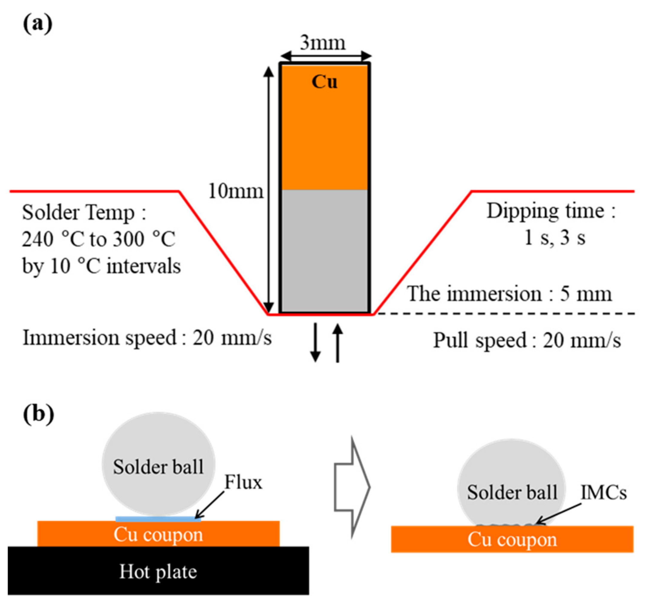
2. Materials and Methods

The effects of Cr addition to a Sn-0.7Cu solder on the nucleation and growth rate of Cu6Sn5 IMCs under various dipping times and temperatures were elucidated using a Sn-0.7Cu-0.2Cr solder. The experiments were also performed under the same conditions using a Sn-0.7Cu solder, and the results were compared. To measure the melting temperature levels of the two solders, differential scanning calorimetry (DSC) equipment (DSC-Q100, TA Inst., New Castle, DE, USA) was used. For testing, approximately 8 mg samples of both solder alloys were used. Measurement conditions were stabilized at 50 °C, then heated to 300 °C at a rate of 10 °C/min, and cooled at the same rate. The melting point of each solder was measured using the heat absorption and exothermic reaction characteristics based on the solder composition. The samples were fabricated by initially polishing the surface of a Cu coupon size (10 × 3 × 1 mm) to a 0.3 µm finish. Subsequently, the Cu coupon was cleaned with ethanol via ultrasonication. Thereafter, a rosin mildly activated (RMA)-type flux (CVP-390, Alpha Assembly Sol., South Plainfield, NJ, USA) was applied on the Cu surface. The samples were then dipped in a bath that contained 300 g of solder using a wetting balance tester (SWB-2, Malcom Co., Ltd., Tokyo, Japan). The schematic diagram of the dipping test, with the dipping conditions, is presented in Figure 1. The bath temperature was varied from 240 to 300 °C, and dipping was performed for 1 and 3 s at intervals of 10 °C. Subsequently, the samples were air cooled. After the molten solder reached the test temperature, it was maintained at this temperature for 10 min to reduce the temperature deviation. The solder in the bath was replaced after each test to prevent changes in its composition. Afterwards, to observe the Cu6Sn5 IMCs, Sn was etched with the NHO3 3% + HCL 2% + C2H5OH 95% solution and its top view was observed using the field emission scanning electron microscope (FE-SEM; Inspect F, FEI Co. Hillsboro, OR, USA) and energy-dispersive spectroscopy (EDS; Superdry, Thermo Noran Inc., Waltham, MA, USA). In addition, the number of Cu6Sn5 grains per unit area and their average size were measured. Moreover, cross-sectional images of Cu6Sn5 IMC were observed using FE-SEM. The shape and microstructure of the Cr compound were observed using an electron probe micro-analyzer (EPMA; JXA-8530F, JEOL Ltd., Tokyo, Japan) and a transmission electron microscope (TEM; JEM-2100F, JEOL Ltd., Tokyo, Japan). A TEM lamella sample of a specific region containing a Cr compound was prepared via the in situ lift-out method using a focused ion beam (FIB, JIB-4500, JEOL Ltd., Tokyo, Japan). A FIB milled TEM lamella sample was mounted on the Cu grid. Prior to FIB milling, a 2 µm carbon layer was deposited on the cross-sectional sample surface. The Cr compound was analyzed via the TEM bright field (BF) image and selected area electron diffraction (SAED) pattern. To measure the shear strength of the solder joint over the bonding temperature and time, a 300 µm solder ball was bonded to the Cu coupon. Bonding was carried out for 1 and 3 s at reaction temperatures of 240, 260, 280, and 300 °C. In this process, a RMA type flux was used to remove the oxide film of the Cu coupons. The schematic of the ball shear test setup is presented in Figure 2. The tests were conducted using a ball shear tester (Dage 4000 HS; Nordson Co., Aylesbury, Buckinghamshire, UK). The shear height for the test was 50 µm, while the shear speeds were 0.01 and 1 m/s. The shear force was estimated based on the average of at least 20 trials. The fracture surfaces after the shear test were observed using the FE-SEM.

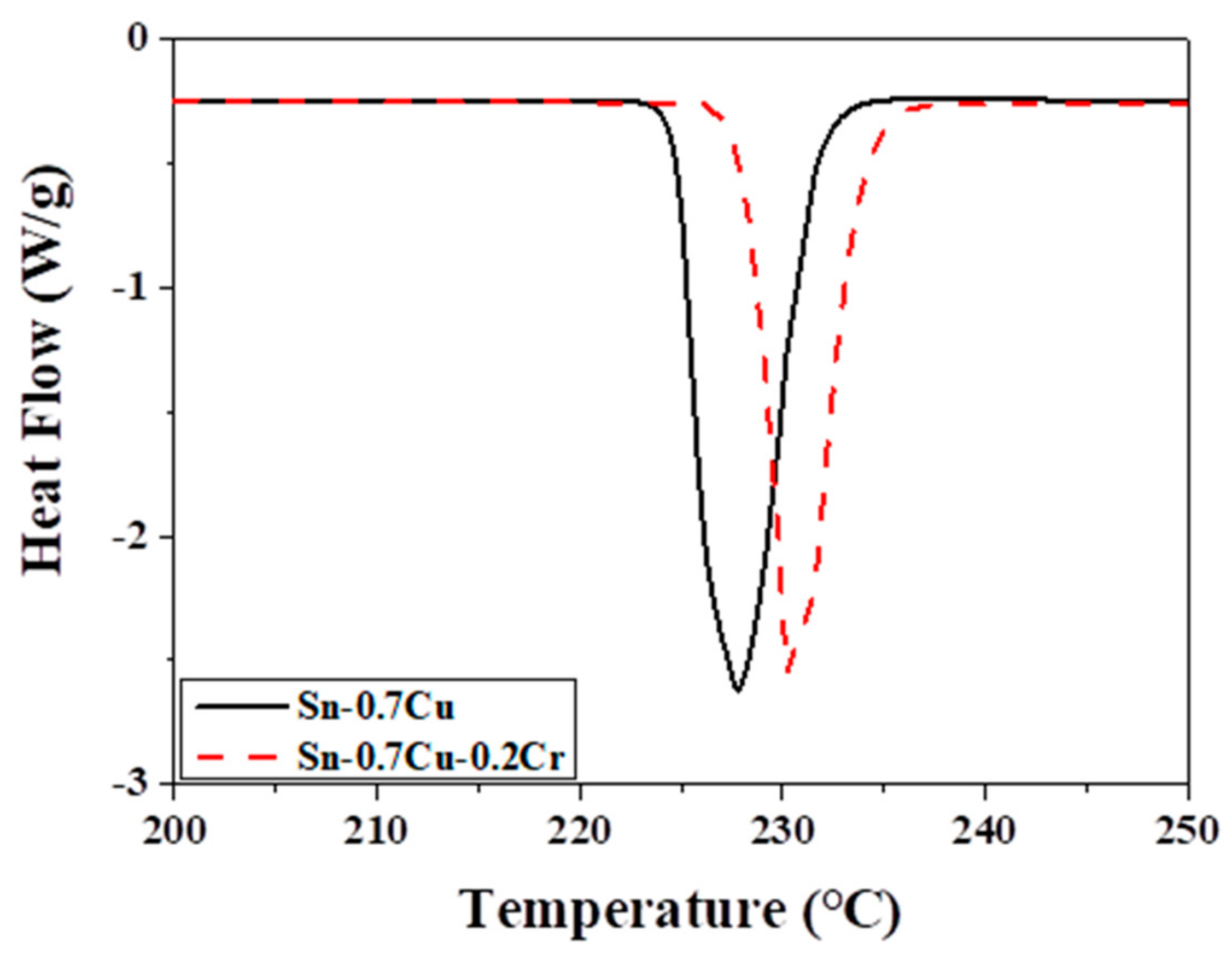
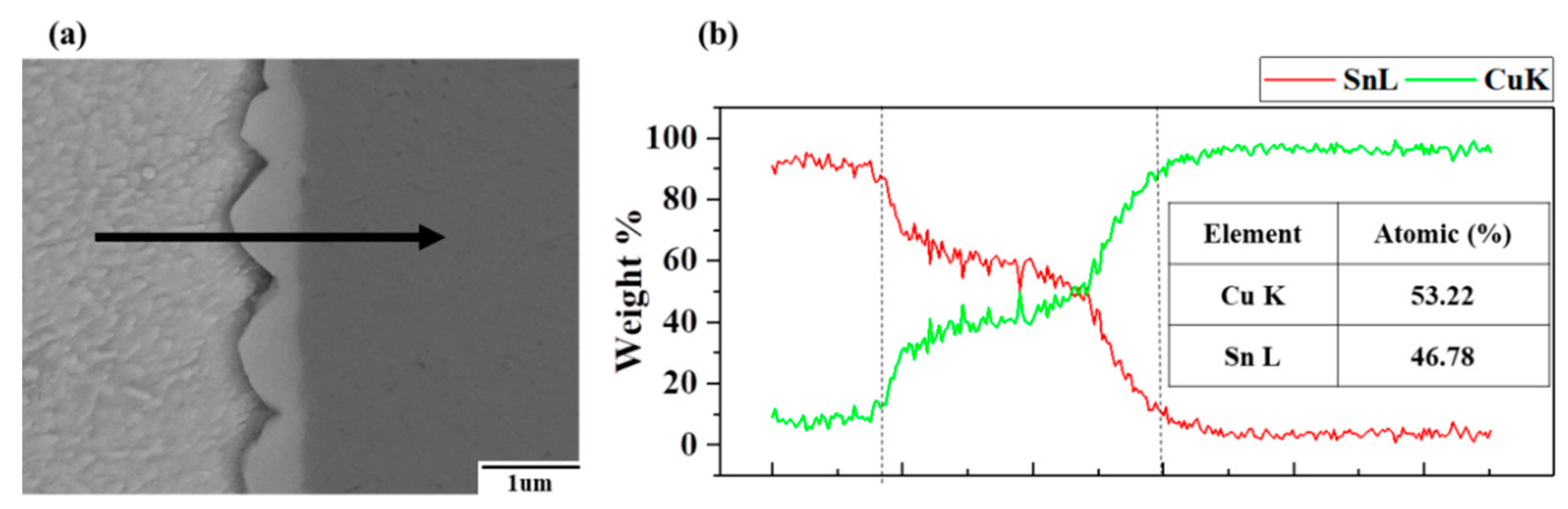
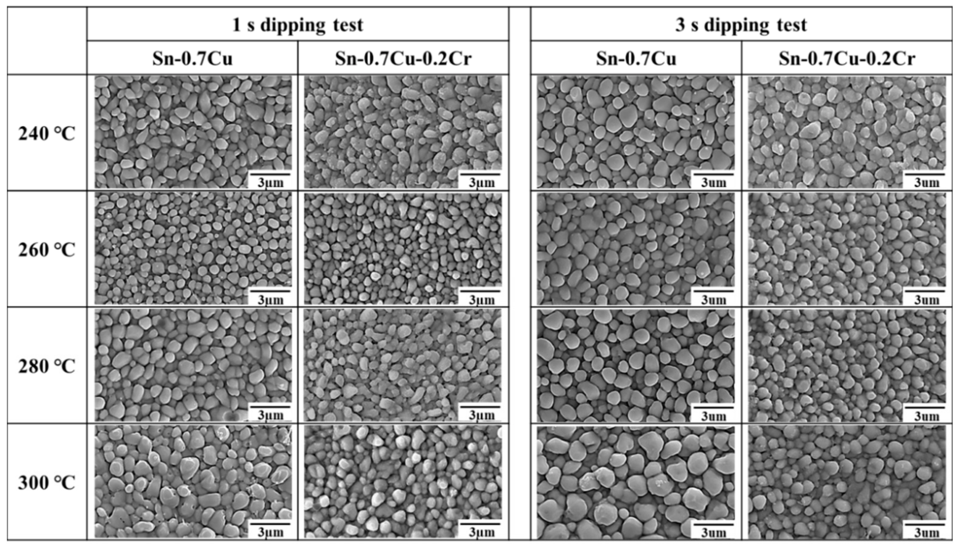
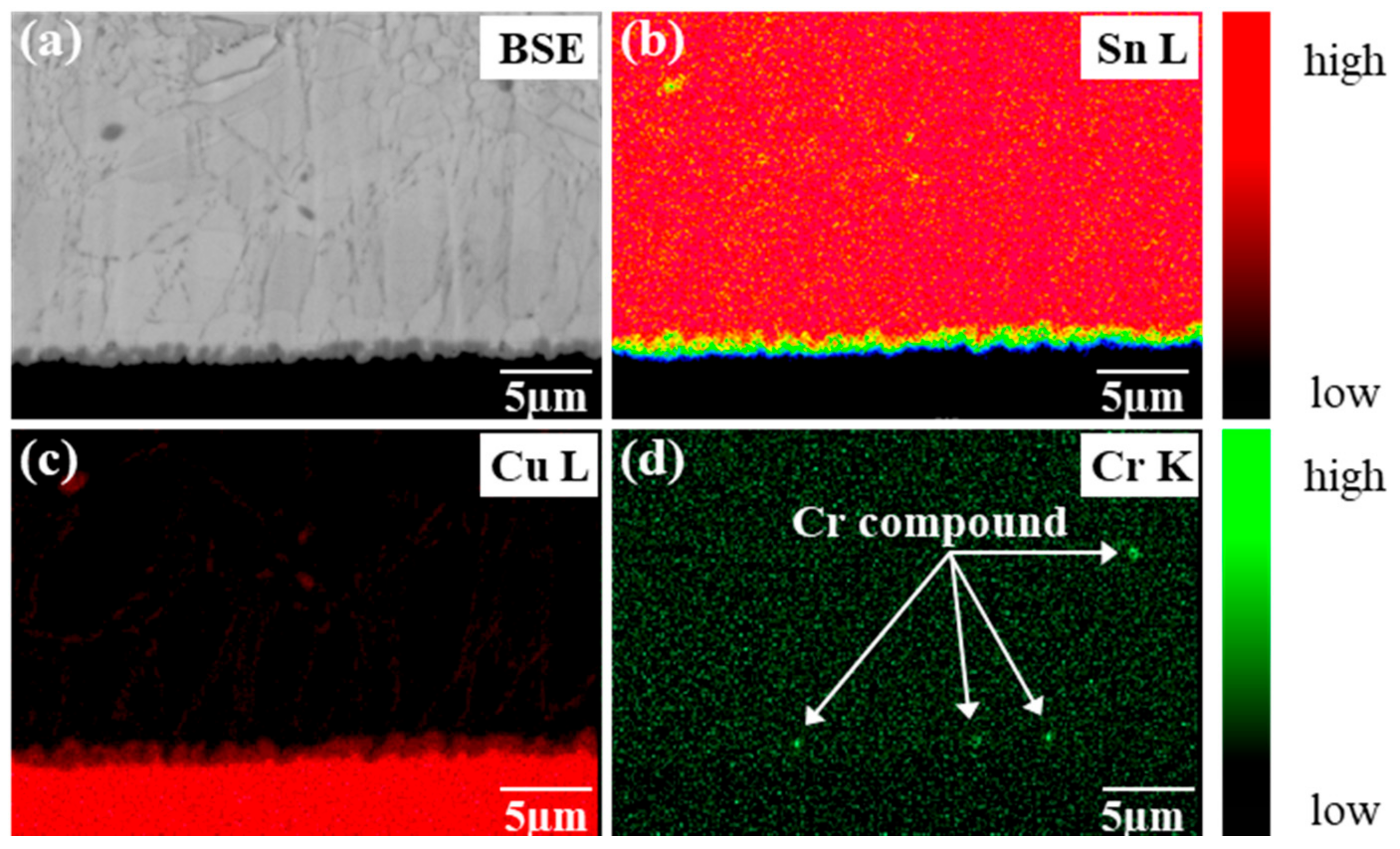
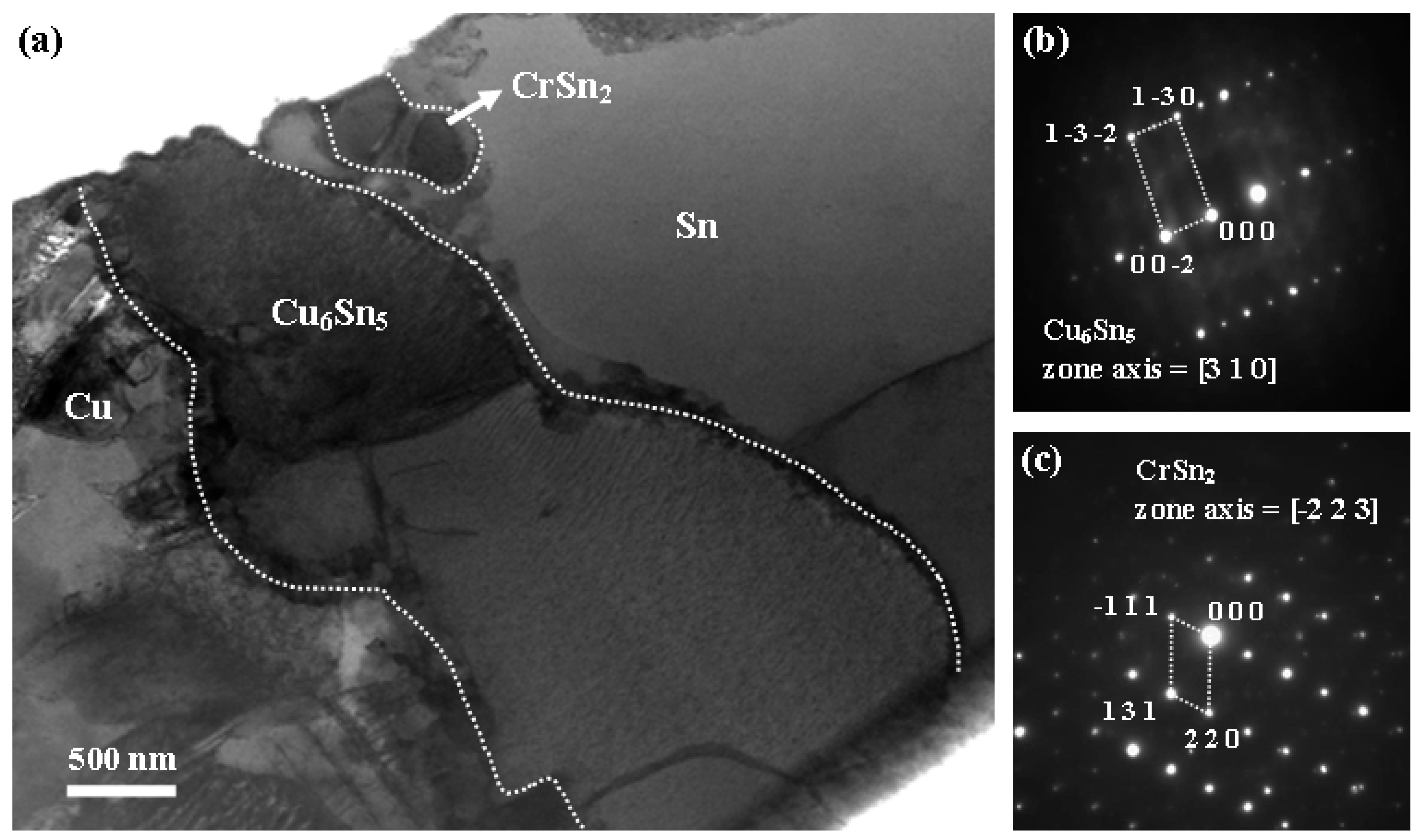
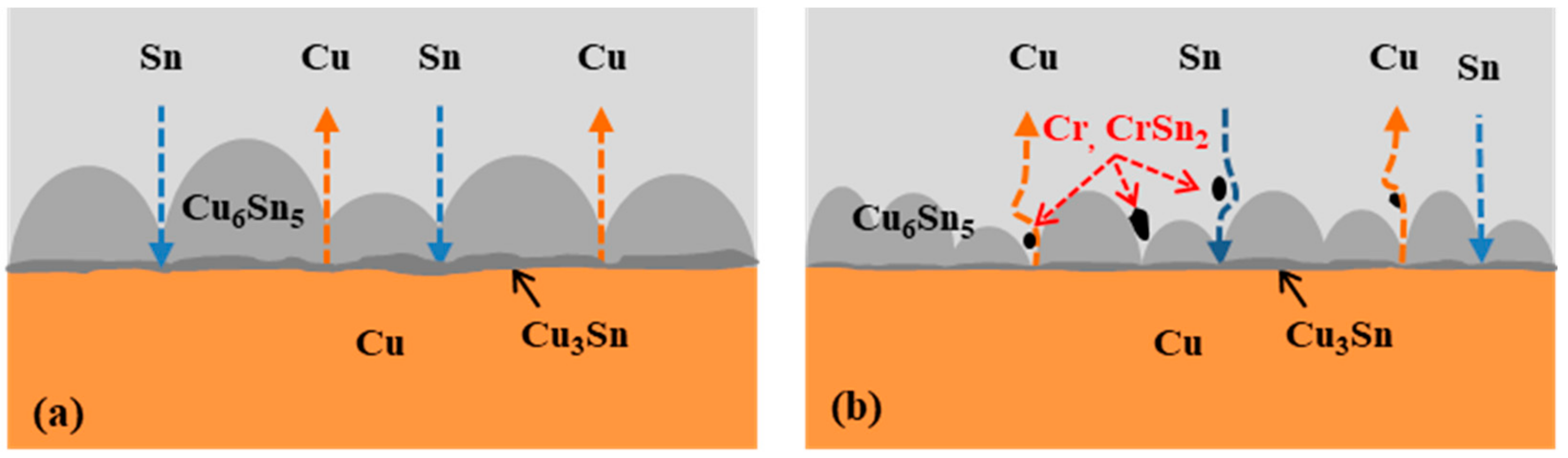
3. Results and Discussion

DSC results are shown in Figure 3. The measured melting temperatures of Sn-0.7Cu and Sn-0.7Cu-0.2Cr solders were 227.8 and 230.7 °C, respectively. The addition of Cr to Sn-0.7Cu solder increased the melting temperature by approximately 3 °C due to the reduced supercooling.
Initially, Cu6Sn5 is precipitated at the interface between the solder and the Cu substrate in a Cu-Sn soldering system. Subsequently, Cu3Sn is precipitated at the interface between Cu6Sn5 and the Cu substrate. The Cu–Sn phase diagram indicated the existence of the Cu41Sn and Cu10Sn3 phases at temperatures exceeding those for the reflow process. Furthermore, the Cu6Sn5 and Cu3Sn phases existed at <350 °C [21,22,23]. Figure 4 shows the SEM line scan images of the IMCs that were observed after immersing the Cu coupon in the Sn-0.7Cu-0.2Cr solder at 300 °C for 3 s. Scallop-like IMC layers were formed after the dipping test, and the EDS analysis confirmed the formation of the Cu6Sn5 IMC. The presence of Cu3Sn was not detected via SEM owing to the low dipping time.
Figure 5 shows the cross-sectional images of the Cu coupons that were dipped in the Sn-0.7Cu and Sn-0.7Cu-0.2Cr solder ports for 1 and 3 s at 240–300 °C. Scallop-shaped Cu6Sn5 IMCs were observed in both solders. The size of the IMCs increased as the dipping time increased. The Cu6Sn5 IMCs were small and thin at the low reaction temperatures owing to the high nucleation rate. The size and thickness of the Cu6Sn5 IMCs increased as the temperature increased owing to the increase in the nucleus growth rate [24]. Furthermore, the IMCs in the Sn-0.7Cu-0.2Cr solder joint were smaller than the IMCs in the Sn-0.7Cu solder joint at all the reaction temperatures. The shape of the IMCs in both the solder joints transformed from scallop-like to round as the reaction temperature increased. The growth of these round IMCs was clearly observed at 3 s of dipping.
Figure 6 shows the IMC thicknesses at various reaction temperatures. The thicknesses were measured after dipping the Cu coupons in the Sn-0.7Cu and Sn-0.7Cu-0.2Cr solder ports for 1 and 3 s at 240–300 °C. The thickness of the IMCs increased as the solder temperature and the dipping time increased. The IMCs in the Sn-0.7Cu-0.2Cr solder were approximately 0.3 µm-thinner than those in the Sn-0.7Cu solder at all the reaction temperatures.
Figure 7 shows the Cu6Sn5 IMCs grain images observed after dipping the Cu coupon into the Sn-0.7Cu and Sn-0.7Cu-0.2Cr solders under various melting temperature conditions for 1 and 3 s. Thus, the changes in the joints with the variation in the solder composition, dipping temperature, and dipping time were analyzed. The sizes of the IMCs in both solders decreased slightly as the temperature increased from 240 to 260 °C. The smallest IMCs were observed at 260 °C. The grain size of the IMCs increased as the temperature exceeded 260 °C. The IMC grains in the Sn-0.7Cu solder were larger than those in the Sn-0.7Cu-0.2Cr solder at all the reaction temperatures. The addition of Cr decreased the supercooling degree and promoted nucleation, thereby lowering the particle size [25]. The sizes of the Cu6Sn5 IMCs in both solders were higher when dipped for 3 s compared to those dipped for 1 s. Furthermore, the particle sizes of the Cu6Sn5 IMCs increased over time at the same temperature [26].
Figure 8 shows the number of Cu6Sn5 IMC grains per unit area (µm2) and the average particle size of the Cu6Sn5 IMCs formed at various reaction temperatures. The particle size of the IMCs decreased slightly as the temperature increased from 240 to 260 °C, irrespective of the dipping time and solder composition. The smallest Cu6Sn5 IMCs were observed at 260 °C. The size of the IMC grains increased as the temperature exceeded 260 °C. The particle size of the IMCs in the Sn-0.7 Cu solder was approximately 12% higher than that of the IMCs in the Sn-0.7Cu-0.2Cr solder. Furthermore, the particle sizes when the dipping time was 3 s were larger than they were when the dipping time was 1 s. The initial growth rate of the IMC particles was high. However, the growth rate decreased as the surface area of the unreacted copper decreased. The formation of IMCs between Sn and Cu also lowered the growth rate. The inverse C shapes of the obtained curves were consistent with the previous results of the nucleation theory [27].
Figure 9 shows an EPMA mapping image for the samples that were dipped in the Sn-0.7Cu-0.2Cr solder at 300 °C for 3 s. The results revealed the presence of a Cr compound in the Sn-0.7Cu-0.2Cr solder. A high quantity of this compound was observed at the interface between the IMCs and the interior of the solder.
Figure 10a shows TEM and SAED pattern images of Cr compounds and interfacial Cu6Sn5 IMCs. The IMCs that were generated at the interface were identified as Cu6Sn5 using the SAED pattern (Figure 10b). No stable IMCs were detected in the Cr-Sn binary phase diagram. However, the presence of other metastable compounds was reported in previous studies [28,29]. The SAED patterns of the Cr-Sn compound in Figure 10c were consistent with the reported crystal structure of the orthogonal CrSn2.
Figure 11 shows the diffusion behaviors of Cu and Sn in the Sn-0.7Cu/Cu and Sn-0.7Cu-0.2Cr/Cu systems. The Cu6Sn5 IMC was formed via the interdiffusion of Cu and Sn. The precipitation of additional elemental materials at the grain boundary impeded the migration of Cu into the Sn matrix, thereby lowering the diffusion rate. The existence of the Cr or CrSn2 IMCs at the interface suppressed the nucleation of the Cu6Sn5 IMCs. The CrSn2 IMCs that were produced during the fabrication of the alloy were precipitated near the IMC layers and dispersed. Moreover, the existence of some products was detected at the Cu6Sn5 grain boundary [17]. These results suggested that the addition of Cr to the Sn-0.7Cu solder effectively prevented the increase in the thickness of the Cu6Sn5 IMCs.
The shear strengths of the solder joints, for different junction temperatures, dipping times, and solder compositions, are presented in Figure 12. The shear strength of the Sn-0.7Cu-0.2Cr solder joint was approximately 80 gf higher than that of the Sn-0.7Cu solder joint at the relatively low shear speed of 0.01 m/s, under all reaction temperatures. The shear strength of both solder joints at a dipping time of 1 s were slightly higher than those at a dipping time of 3 s. The deterioration inside the solder following the increase in the dipping duration resulted in the slight lowering of the shear strength. When the shear speed was high (1 m/s), the shear strength of the Sn-0.7Cu solder joint was higher than that of the Sn-0.7Cu-0.2Cr solder joint at low reaction temperatures. This was attributed to the slower growth of the IMCs in the Sn-0.7Cu-0.2Cr solder as compared to that of the IMCs in the Sn-0.7Cu solder at the low reaction temperatures. Consequently, the Sn-0.7Cu-0.2Cr solder joints were not robust under this condition. However, robust Sn-0.7Cu-0.2Cr solder joints were formed at the reaction temperatures above 260 °C. Therefore, the Sn-0.7Cu-0.2Cr and Sn-0.7Cu solder joints yielded similar shear strengths above 260 °C. The shear strength of the Sn-0.7Cu-0.2Cr solder joint was higher than that of the Sn-0.7Cu solder joint above 280 °C. This was due to the fact that the shape of the IMCs in the Sn-0.7Cu-0.2Cr solder joint was more scallop-like compared to that of the IMCs in the Sn-0.7Cu solder. The presence of these scallop-like IMCs resulted in the high shear strength of the Sn-0.7Cu-0.2Cr solder joint under the high-speed shear conditions. The increase in the shear strength following the increase in the shear speed was reported in previous studies [30,31].
Figure 13 shows the tensile strength of Sn-0.7Cu and Sn-0.7Cu-0.2Cr solders. When Cr was added, the tensile strength increased by approximately 12%. This is believed to increase the tensile strength by acting as second-phase particles of CrSn2 or Cr dispersed in the solder, thus blocking the propagation of cracks generated in the tensile strength test. Accordingly, the shear strength of Sn-0.7Cu-0.2Cr solder was higher than that of Sn-0.7Cu at a shear rate of 0.01 m/s.
Figure 14 shows the fracture surfaces of the Sn-0.7Cu and Sn-0.7Cu-0.2Cr solders at various reaction temperatures. The ductile fracture occurred at the low shear rate of 0.01 m/s. When the shear rate was 1 m/s, a complex fracture with both ductile and brittle characteristics was observed. At low shear rates, all fractures are stress relieved by deformation inside the bulk solder, so the ductile fracture dominates. As the shear rate increases, a large amount of stress accumulates at the interface due to the rapid deformation inside the solder, causing breakage along the solder/IMC interface. The stress may be concentrated in the solder/IMC region due to the mismatch of the modulus of elasticity between the rough interface and the dissimilar material [32]. In general, in the thermal aging test or thermal cycle test, delamination occurs between heterogeneous IMCs or at the IMC/interface due to the excessive growth of IMCs and kirkendall voids [33,34,35]. In this study, the growth of Cu6Sn5 IMC increased as the dipping temperature and time increased. Accordingly, the brittle fracture rate increased.
Figure 15 shows the statistics of the fracture modes of the solder joints at shear speeds of 0.01 and 1 m/s. When the shear speed was 1 m/s, the brittle fracture rate in the Sn-0.7Cu solder was higher than that in the Sn-0.7Cu-0.2Cr solder. The brittle fracture rate in the Sn-0.7Cu-0.2Cr solder remained low owing to the relatively thin interfacial IMCs. IMCs are typically fragile, and the increase in their thickness results in an increase in the number of brittle areas. Consequently, the fragility of IMCs increases with the increase in thickness [36]. The high shear strength of the Sn-0.7Cu-0.2Cr solder was attributed to the influence of the shear strength of the Cr or CrSn2 compounds that existed inside and near the surface of the solder. It was concluded that the shear strengths of the Sn-0.7Cu-0.2Cr solder joints was significantly higher than those of the Sn-0.7Cu solder joints in this study.

4. Conclusions

The nucleation kinetics and growth rate of Cu6Sn5 IMCs in a Sn-0.7Cu-0.2Cr solder were investigated in this study. Additionally, the mechanical properties of the Sn-0.7Cu-0.2Cr solder joints were characterized. The study results are summarized as follows:
(1)
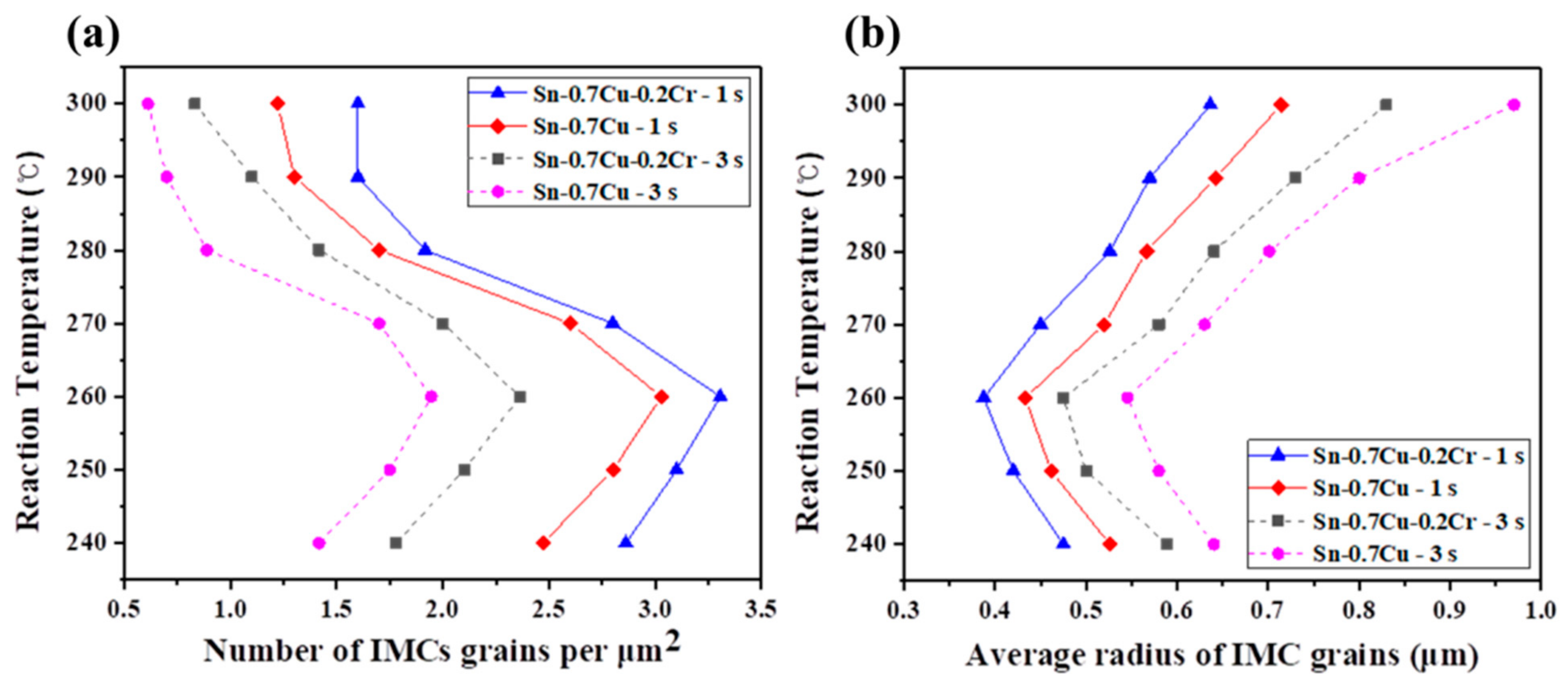
The samples revealed that the grain size of the Cu6Sn5 IMCs in both solders was minimum at 260 °C. The grain size increased as the temperature increased to 280 and 300 °C. The grain size of the Cu6Sn5 IMCs in the Sn-0.7Cu-0.2Cr solder was lower than that of Cu6Sn5 IMCs in the Sn-0.7Cu solder, at all dipping times and temperatures. The addition of Cr decreased the supercooling degree and promoted nucleation, thereby lowering the particle size.
(2)
The Sn-0.7Cu-0.2Cr solder/Cu joints suppressed IMC growth more effectively than the Sn-0.7Cu solder/Cu joints. This suppressed the interfacial IMC growth by interfering with the diffusion of Sn and Cu by CrSn2 IMC present at the interface.
(3)
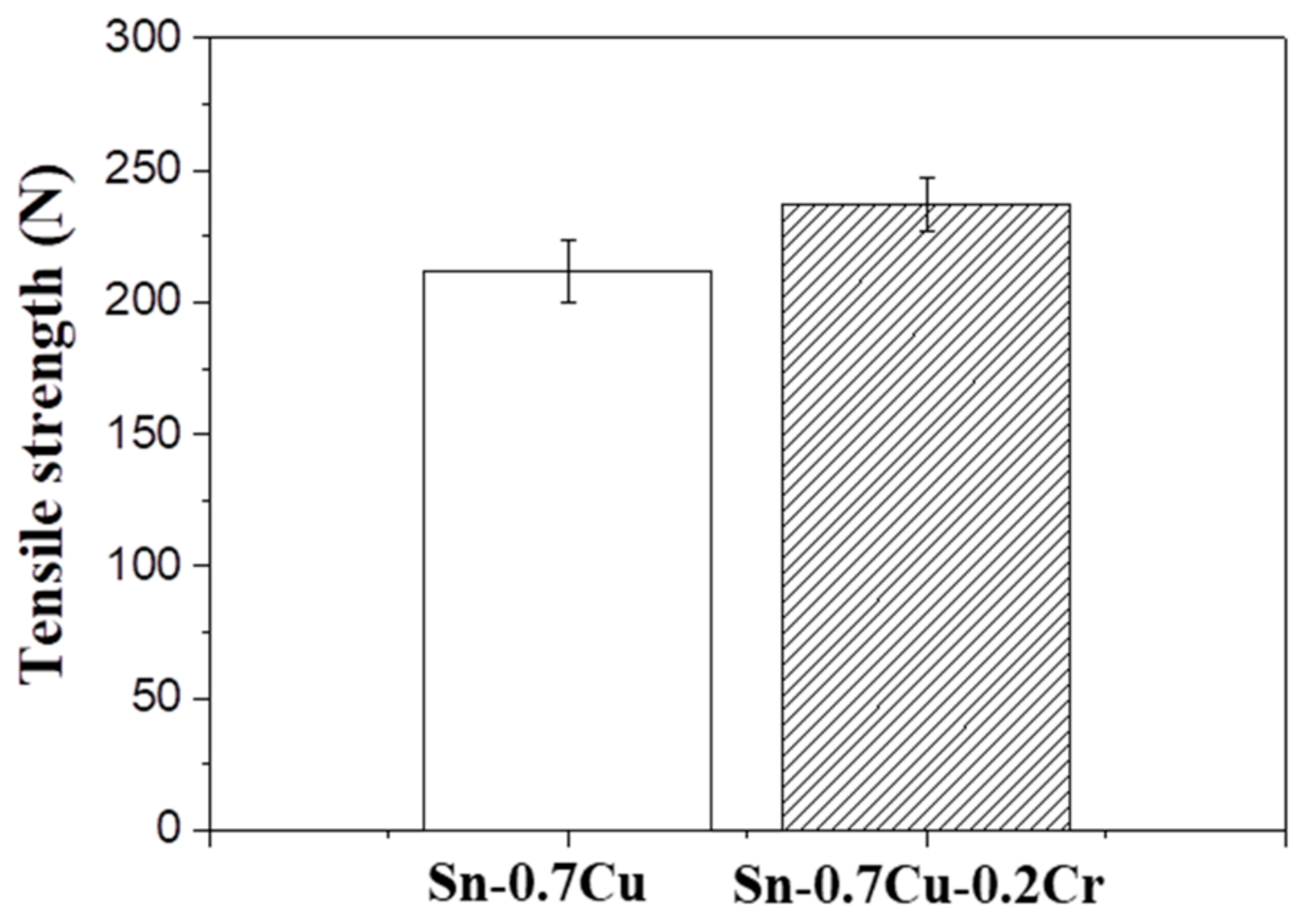
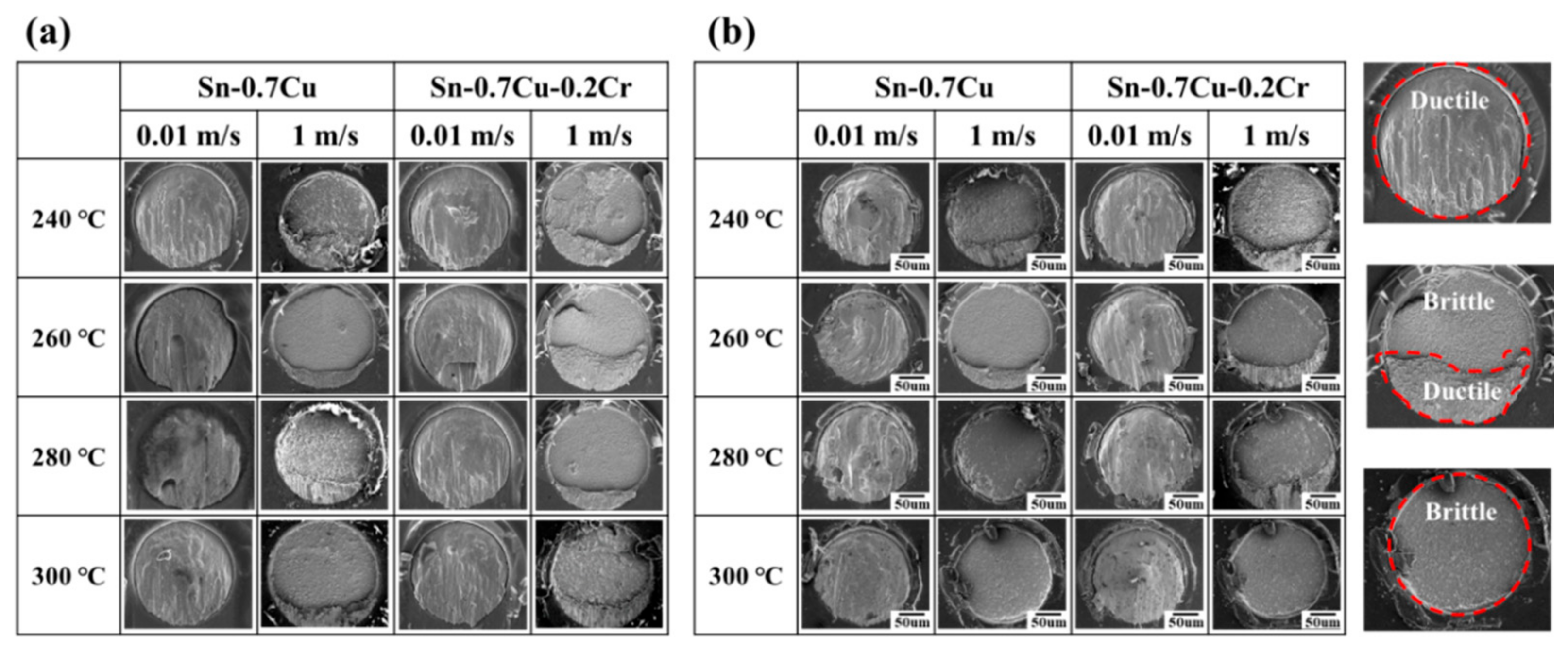
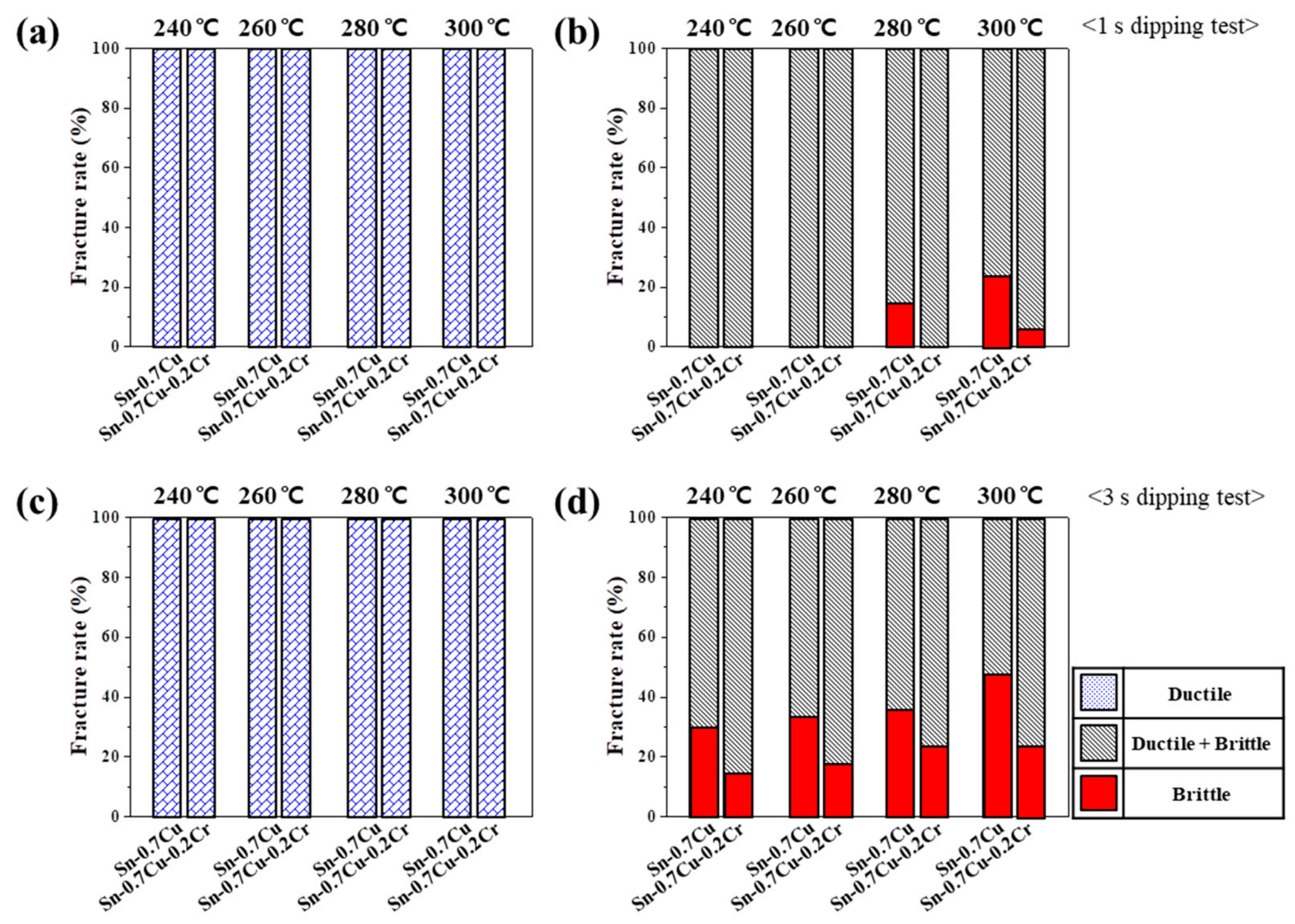
In the shear test, the fracture occurred inside the solder at low shear rates, and at high shear rates at the solder/IMC interface or IMC/substrate interface. The results of the low shear strength tests revealed that the shear strengths of the Sn-0.7Cu-0.2Cr solder joints were higher than those of the Sn-0.7Cu solder joints. The high shear strength of the Sn-0.7Cu-0.2Cr solder joints was attributed to the shear strength of the CrSn2 compounds inside and near the surface of the solder. In the high-speed shear test, the brittle fracture increased as the thickness of IMC increased.

Author Contributions

Conceptualization, D.-Y.Y. and D.-J.B.; Data curation, J.S. and Y.-H.K.; Formal analysis, M.-S.K. and J.B.; Investigation, J.S. and Y.-H.K.; Methodology, D.-Y.Y. and M.-S.K.; Project administration, J.B.; Writing—original draft, J.S.; Writing—review & editing, J.B. All authors have read and agreed to the published version of the manuscript.

Funding

This research received no external funding.

Data Availability Statement

Data sharing is not applicable to this article.

Conflicts of Interest

The authors declare no conflict of interest.

References

  1. Kang, S.K. Lead (Pb)-free solders for electronic packaging. J. Electron. Mater. 1994, 23, 701–707. [Google Scholar] [CrossRef]
  2. Leng, E.P.; Ding, M.; Ling, W.T.; Amin, N.; Ahmad, I.; Lee, M.Y.; Haseeb, A.S.M.A. A study of SnAgNiCo vs Sn3.8AgO.7Cu C5 lead free solder alloy on mechanical strength of BGA solder joint. In Proceedings of the 2008 10th Electronics Packaging Technology Conference, Singapore, 9–12 December 2008; pp. 588–594. [Google Scholar]
  3. Kim, J.M.; Jeong, M.H.; Yoo, S.; Park, Y.B. Effect of interfacial microstructures on the bonding strength of Sn-3.0Ag-0.5Cu Pb-free solder bump. Jpn. J. Appl. Phys. 2012, 51, 05EE06. [Google Scholar] [CrossRef]
  4. Park, J.M.; Kim, S.H.; Jeong, M.H.; Park, Y.B. Effect of Cu-Sn intermetallic compound reactions on the Kirkendall void Growth characteristics in Cu/Sn/Cu microbumps. Jpn. J. Appl. Phys. 2014, 53, 1–5. [Google Scholar] [CrossRef] [Green Version]
  5. Tu, K.N.; Thompson, R.D. Kinetics of interfacial reaction in bimetallic CuSn thin films. Acta Metall. 1982, 30, 947–952. [Google Scholar] [CrossRef]
  6. Deng, X.; Piotrowski, G.; Williams, J.J.; Chawla, N. Influence of Initial Morphology and Thickness of Cu6Sn5 and Cu3Sn Intermetallics on Growth and Evolution during Thermal Aging of Sn-Ag Solder/Cu Joints. J. Electron. Mater. 2003, 32, 1403–1413. [Google Scholar] [CrossRef] [Green Version]
  7. Mu, D.; Huang, H.; Nogita, K. Anisotropic mechanical properties of Cu6Sn5 and (Cu,Ni)6Sn5. Mater. Lett. 2012, 86, 46–49. [Google Scholar] [CrossRef]
  8. Deng, X.; Sidhu, R.S.; Johnson, P.; Chawla, N. Influence of reflow and thermal aging on the shear strength and fracture behavior of Sn-3.5Ag solder/Cu joints. Metall. Mater. Trans. A Phys. Metall. Mater. Sci. 2005, 36, 55–64. [Google Scholar] [CrossRef]
  9. Chan, Y.C.; So, A.C.K.; Lai, J.K.L. Growth kinetic studies of Cu – Sn intermetallic compound and its effect on shear strength of LCCC SMT solder joints. Mater. Sci. Eng B 1998, 55, 5–13. [Google Scholar] [CrossRef]
  10. Limaye, P.; Labie, R.; Vandevelde, B.; Vandepitte, D.; Verlinden, B. Creep behavior of mixed SAC 405/ SnPb soldered assemblies in shear loading. In Proceedings of the 2007 9th Electronics Packaging Technology Conference, Singapore, 10–12 December 2007; pp. 703–712. [Google Scholar]
  11. Chen, X.; Li, M.; Ren, X.; Mao, D. Effects of alloying elements on the characteristics of Sn-Zn lead-free solder. In Proceedings of the 2005 6th International Conference on Electronic Packaging Technology, Shenzhen, China, 30 August–2 September 2005. [Google Scholar]
  12. Lin, K.L.; Liu, P.C.; Song, J.M. Wetting interaction between Pb-free Sn-Zn series solders and Cu, Ag substrates. In Proceedings of the 54th Electronic Components and Technology Conference, Las Vegas, NV, USA, 4 June 2004; Volume 2, pp. 1310–1313. [Google Scholar]
  13. Wang, J.; Wen, L.; Zhou, J.; Chung, M. Mechanical properties and joint reliability improvement of Sn-Bi alloy. In Proceedings of the 2011 IEEE 13th Electronics Packaging Technology Conference, Singapore, 7–9 December 2011; Volume 8823, pp. 492–496. [Google Scholar]
  14. Cho, M.G.; Kang, S.K.; Shih, D.Y.; Lee, H.M. Effects of minor additions of Zn on interfacial reactions of Sn-Ag-Cu and Sn-Cu solders with various Cu substrates during thermal aging. J. Electron. Mater. 2007, 36, 1501–1509. [Google Scholar] [CrossRef]
  15. Hu, F.Q.; Zhang, Q.K.; Jiang, J.J.; Song, Z.L. Influences of Ag addition to Sn-58Bi solder on SnBi/Cu interfacial reaction. Mater. Lett. 2018, 214, 142–145. [Google Scholar] [CrossRef]
  16. Li, J.Y.; Peng, J.; Wang, R.C.; Feng, Y.; Peng, C.Q. Effects of Co addition on shear strength and interfacial microstructure of Sn–Zn–(Co)/Ni joints. J. Mater. Sci. Mater. Electron. 2018, 29, 19901–19908. [Google Scholar] [CrossRef]
  17. Bang, J.; Yu, D.Y.; Ko, Y.H.; Son, J.H.; Nishikawa, H.; Lee, C.W. Intermetallic compound growth between Sn-Cu-Cr lead-free solder and Cu substrate. Microelectron. Reliab. 2019, 99, 62–73. [Google Scholar] [CrossRef]
  18. Santra, S.; Davies, T.; Matthews, G.; Liu, J.; Grovenor, C.R.M.; Speller, S.C. The effect of the size of NbTi filaments on interfacial reactions and the properties of InSn-based superconducting solder joints. Mater. Des. 2019, 176, 107836. [Google Scholar] [CrossRef]
  19. Zhang, X.; Hu, X.; Jiang, X.; Li, Y. Effect of Ni addition to the Cu substrate on the interfacial reaction and IMC growth with Sn3.0Ag0.5Cu solder. Appl. Phys. A Mater. Sci. Process. 2018, 124, 315. [Google Scholar] [CrossRef]
  20. Zhang, S.; Yang, M.; Wu, Y.; Du, J.; Lin, T.; He, P.; Huang, M.; Paik, K.W. A Study on the Optimization of Anisotropic Conductive Films for Sn-3Ag-0.5Cu-Based Flex-on-Board Application at a 250 °C Bonding Temperature. IEEE Trans. Compon. Packag. Manuf. Technol. 2018, 8, 383–391. [Google Scholar] [CrossRef]
  21. Nogita, K.; Gourlay, C.M.; Nishimura, T. Cracking and phase stability in reaction layers between Sn-Cu-Ni solders and Cu substrates. Jom 2009, 61, 45–51. [Google Scholar] [CrossRef]
  22. Chen, S.W.; Wu, S.H.; Lee, S.W. Interfacial reactions in the Sn-(Cu)/Ni, Sn-(Ni)/Cu, and Sn/(Cu,Ni) systems. J. Electron. Mater. 2003, 32, 1188–1194. [Google Scholar] [CrossRef]
  23. Chen, S.W.; Chen, C.M.; Liu, W.C. Electric current effects upon the Sn\Cu and Sn\Ni interfacial reactions. J. Electron. Mater. 1998, 27, 1193–1198. [Google Scholar] [CrossRef]
  24. Park, M.S.; Arroyave, R. Formation and growth of intermetallic compound Cu6Sn5 at early stages in lead-free soldering. J. Electron. Mater. 2010, 39, 2574–2582. [Google Scholar] [CrossRef] [Green Version]
  25. Kotadia, H.R.; Mokhtari, O.; Clode, M.P.; Green, M.A.; Mannan, S.H. Intermetallic compound growth suppression at high temperature in SAC solders with Zn addition on Cu and Ni-P substrates. J. Alloy. Compd. 2012, 511, 176–188. [Google Scholar] [CrossRef]
  26. Yang, M.; Cao, Y.; Joo, S.; Chen, H.; Ma, X.; Li, M. Cu6Sn5 precipitation during Sn-based solder/Cu joint solidification and its effects on the growth of interfacial intermetallic compounds. J. Alloy. Compd. 2014, 582, 688–695. [Google Scholar] [CrossRef]
  27. Gagliano, R.A.; Ghosh, G.; Fine, M.E. Nucleation kinetics of Cu6Sn5 by reaction of molten tin with a copper substrate. J. Electron. Mater. 2002, 31, 1195–1202. [Google Scholar] [CrossRef]
  28. Wölpl, T.; Jeitschko, W. Crystal structures of VSn2, NbSn2 and CrSn2 with Mg2Cu-type structure and NbSnSb with CuAl2-type structure. J. Alloy. Compd. 1994, 210, 185–190. [Google Scholar] [CrossRef]
  29. Larsson, A.K.; Lidin, S. The crystal structures of the closely related CrSn2, NiCr5Sn12 and NiCr3Sn8 phases. J. Alloy. Compd. 1995, 221, 136–142. [Google Scholar] [CrossRef]
  30. Kim, J.W.; Kim, D.G.; Jung, S.B. Mechanical strength test method for solder ball joint in BGA package. Met. Mater. Int. 2005, 11, 121–129. [Google Scholar] [CrossRef]
  31. Kim, J.W.; Jang, J.K.; Ha, S.O.; Ha, S.S.; Kim, D.G.; Jung, S.B. Effect of high-speed loading conditions on the fracture mode of the BGA solder joint. Microelectron. Reliab. 2008, 48, 1882–1889. [Google Scholar] [CrossRef]
  32. Hu, X.; Xu, T.; Keer, L.M.; Li, Y.; Jiang, X. Shear strength and fracture behavior of reflowed Sn3.0Ag0.5Cu/Cu solder joints under various strain rates. J. Alloy. Compd. 2017, 690, 720–729. [Google Scholar] [CrossRef]
  33. Gain, A.K.; Zhang, L. Harsh service environment effects on the microstructure and mechanical properties of Sn–Ag–Cu-1 wt% nano-Al solder alloy. J. Mater. Sci. Mater. Electron. 2016, 27, 11273–11283. [Google Scholar] [CrossRef]
  34. Cao, C.; Zhang, K.; Shi, B.; Wang, H.; Zhao, D.; Sun, M.; Zhang, C. The interface microstructure and shear strength of Sn2.5Ag0.7Cu0.1RExNi/Cu solder joints under thermal-cycle loading. Metals 2019, 9, 518. [Google Scholar] [CrossRef] [Green Version]
  35. Qiu, H.; Hu, X.; Li, S.; Wan, Y.; Li, Q. Shear strength and fracture surface analysis of lead-free solder joints with high fraction of IMCs. Vacuum 2020, 180, 109611. [Google Scholar] [CrossRef]
  36. Yoon, J.W.; Noh, B.I.; Lee, Y.H.; Lee, H.S.; Jung, S.B. Effects of isothermal aging and temperature-humidity treatment of substrate on joint reliability of Sn-3.0Ag-0.5Cu/OSP-finished Cu CSP solder joint. Microelectron. Reliab. 2008, 48, 1864–1874. [Google Scholar] [CrossRef]
Figure 1. Schematic of the (a) dipping test and (b) ball shear test sample.
Metals 11 00210 g001
Figure 2. Schematic of the ball shear test.
Metals 11 00210 g002
Figure 3. DSC curve of Sn-0.7Cu and Sn-Cu-0.2Cr solders.
Metals 11 00210 g003
Figure 4. Cross-sectional images and corresponding EDS line scanning results of the intermetallic compounds (IMCs) for 3 s of dipping at 300 °C at Sn-0.7Cu-0.2Cr/Cu: (a) SEM image and (b) EDS results.
Metals 11 00210 g004
Figure 5. Cross-sectional images of the Cu6Sn5 IMCs obtained after dipping the Cu coupon in Sn-0.7Cu and Sn- 0.7Cu-0.2Cr solders at various reaction temperatures.
Metals 11 00210 g005
Figure 6. Thickness of the Cu6Sn5 IMCs at various reaction temperatures.
Metals 11 00210 g006
Figure 7. Top view images of the Cu6Sn5 IMCs at various reaction temperatures at Sn-0.7Cu/Cu and Sn- 0.7Cu-0.2Cr/Cu solders.
Metals 11 00210 g007
Figure 8. (a) Number of Cu6Sn5 IMC grains per unit area (µm2) and the (b) average radius of the Cu6Sn5 IMC grains, at various reaction temperatures.
Metals 11 00210 g008
Figure 9. EPMA electron mapping of the Sn-0.7Cu-0.2Cr solder joint (a) SEM image of the mapping region. Elemental maps of (b) Sn, (c) Cu, (d) Cr.
Metals 11 00210 g009
Figure 10. (a) TEM bright field image of the interfacial microstructure for the Sn-0.7Cu-0.2Cr solder joint. Selected area electron diffraction patterns for (b) Cu6Sn5 and (c) CrSn2.
Metals 11 00210 g010
Figure 11. Schematic of the interdiffusion of Cu and Sn in the (a) Sn-0.7Cu/Cu and (b) Sn-0.7Cu-0.2Cr/Cu systems.
Metals 11 00210 g011
Figure 12. Shear strength of the solder joints at shear speeds of (a) 0.01 and (b) 1 m/s under various reaction temperatures.
Metals 11 00210 g012
Figure 13. Tensile strength of Sn-0.7Cu and Sn-0.7Cu-0.2Cr solders.
Metals 11 00210 g013
Figure 14. Fracture surfaces of the solder joints at dipping times of (a) 1 and (b) 3 s for different shear speeds under various reaction temperatures.
Metals 11 00210 g014
Figure 15. Statistics of the fracture modes of the solder joints at shear speeds of (a,c) 0.01 and (b,d) 1 m/s.
Metals 11 00210 g015
Publisher’s Note: MDPI stays neutral with regard to jurisdictional claims in published maps and institutional affiliations.

