Article

Improved Synaptic Device Properties of HfAlOx Dielectric on Highly Doped Silicon Substrate by Partial Reset Process

Division of Electronics and Electrical Engineering, Dongguk University, Seoul 04620, Korea
*
Author to whom correspondence should be addressed.
Metals 2021, 11(5), 772; https://doi.org/10.3390/met11050772
Submission received: 28 March 2021 / Revised: 7 May 2021 / Accepted: 7 May 2021 / Published: 8 May 2021

Abstract

:
This work demonstrates the synaptic properties of the alloy-type resistive random-access memory (RRAM). We fabricated the HfAlOx-based RRAM for a synaptic device in a neuromorphic system. The deposition of the HfAlOx film on the silicon substrate was verified by X-ray photoelectron spectroscopy (XPS) analysis. It was found that both abrupt and gradual resistive switching could be implemented, depending on the reset stop voltage. In the reset process, the current gradually decreased at weak voltage, and at strong voltage, it tended to decrease rapidly by Joule heating. The type of switching determined by the first reset process was subsequently demonstrated to be stable switching by successive set and reset processes. A gradual switching type has a much smaller on/off window than abrupt switching. In addition, retention maintained stability up to 2000 s in both switching cases. Next, the multiple current states were tested in the gradual switching case by identical pulses. Finally, we demonstrated the potentiation and depression of the Cu/HfAlOx/Si device as a synapse in an artificial neural network and confirmed that gradual resistive switching was suitable for artificial synapses, using neuromorphic system simulation.

1. Introduction

Recently, in the rapidly increasing number of server computers and Internet of Things (IoT) era, there is a demand for the development of higher capacity and faster memory than the conventional memory, such as flash memory [1]. Resistance-change memories such as phase-change RAM (PRAM) [2], magnetic RAM (MRAM) [2], and RRAM are superior to flash memory in terms of operating voltage and operating speed. Especially, PRAM and RRAM have the possibility of securing excellent characteristics by fabricating them vertically beyond the stacking of cross-points in cell structure to achieve the high-density memory [3]. RRAM has been found to have a memory switching effect in a variety of dielectric materials. Basically, low-resistance state (LRS) and high-resistance state (HRS) can be converted according to the applied voltage, and the state, once stored, has a nonvolatile characteristic that is maintained over time [4,5,6,7]. Among a lot of materials, metal oxides like TiO2, HfO2 and Ta2O5 are the most popular resistive switching materials due to their superior memory device behaviors, such as endurance, stability, repeatability, and reproducibility [8,9,10,11,12,13,14,15]. Regarding the resistive change switching effect of metal oxide-based RRAM devices, various mechanisms are known, depending on the resistive switching materials and the electrodes [16]. The conductivity changes as the oxygen increases or decreases for the intrinsic switching in the oxide. In this case, a non-active metal is used for the top and bottom electrodes. The resistive switching occurs by the creation and rupture of a metallic filament when using the metal electrodes with high diffusion ability to the dielectric. These electrochemical metallization effects are commonly observed when using Cu and Ag electrodes [16]. This kind of resistive memory has a fast switching speed but shows low endurance. Especially, Cu is a more complementary metal-oxide-semiconductor (CMOS), compatible when using barrier metals such TaN and Ta [17]. Resistive switching can also be classified depending on the operating polarity. Unipolar resistive switching occurs in the same polarity. The reset process occurs by Joule heating and it is accompanied by high current. Representatively, unipolar resistive switching has been reported a great deal in NiO, TiO2, ZnO, ZrO2, and HfO2 [18,19,20,21,22,23,24,25,26,27]. Although research on URS has been conducted for a long time, the poor distribution of high current, voltage, and resistance values have not been resolved. On the other hand, bipolar resistive switching (BRS), which is commonly found in various materials such as HfO2 and TaO2, can operate at a low current overall and shows better dispersion characteristics. However, a bidirectional selector element is needed for each memory cell in a crossbar array to reduce the sneak current path [28].
In this work, we fabricated the CMOS compatible Cu/HfAlOx/Si memory cells and the device stack was verified by XPS analysis. The alloyed type of device can change the resistive switching characteristics by adjusting the ratio of the elements. For example, as the content of Al with a large band gap increases in the HfAlOx-based stack, the insulated character becomes stronger, which can lower the initial current level [29,30]. We investigated the resistive switching in two switching modes from an HfAlOx-based device. One is abrupt switching behavior and the other is gradual switching behavior. The two switching modes can be adjusted simply by the size of the reset voltage. The tight distribution of resistance values and nonvolatile properties of LRS and HRS in both modes were verified by the retention test. In gradual switching mode, the transient characteristics with multiple states were confirmed by pulse. Finally, the potentiation and depression characteristics were demonstrated to implement synaptic properties for a hardware-based neuromorphic system and a neuromorphic system simulation was conducted.

2. Materials and Methods

Figure 1a shows the schematic of the fabricated Cu/HfAlOx/Si device which was prepared as follows—A-200 nm thick doped poly Si as bottom electrode in RRAM was deposited on silicon substrate by low-pressure chemical vapor deposition (LPCVD). SiH4 and PH3 were used for n-type doped Si. The native oxide (SiO2) was removed by Hydrogen fluoride (HF) chemical solution before the deposition of high-k layer. A 7 nm thick alloyed type HfAlOx film was deposited by atomic layer deposition (ALD). Tetrakis-ethylmethylamino hafnium (TEMAHf) and H2O as precursors were used for the HfO2 layer. Trimethylaluminum (TMA) and H2O were used for Al2O3 layer. Three cycles of HfO2 layer and one cycle of Al2O3 layer were deposited alternately for the HfAlOx alloyed film. A 100-nm thick Cu was deposited by e-beam evaporator into the top contact hole after the attachment of shadow mask including the circular pattern with a diameter of 100 μm. The electrical properties of direct current (DC) I-V curves were measured by a Keithley 4200-SCS semiconductor parameter analyzer (SPA) and pulse measurements were conducted by a 4225-pulse measurement unit (PMU) ultrafast module. For a bias voltage and a pulse input, Cu contacted with a probe tip was controlled while maintaining the ground on the Si bottom electrode. X-ray photoelectron spectroscopy (XPS) depth analysis was conducted, using a Nexsa (ThermoFisher Scientific, Waltham, MA, USA) with a Microfocus monochromatic X-ray source (Al-Kα (1486.6 eV)), a sputter source (Ar+), an ion energy of 2 kV, a sputter area of 1 × 1 mm, a sputter rate of 0.5 nm/s for SiO2, and a beam size of 100 μm.

3. Results and Discussion

The XPS analysis was conducted to confirm the alloyed type HfAlOx film deposited by ALD. Figure 1b,c show Hf 4f and Al 2p spectra after 3 s etching. Hf 4f had two distinct and clear peaks in which the Hf4f7/2 and Hf4f5/2 were centered at 18.74 and 20.27 eV, respectively (Figure 1b) [31]. The raw data of Al 2p was more noisy because it had 3 times fewer deposition cycles than Hf (Figure 1c). However, the peak intensity’s binding energy (75.69 eV) in the fitting curve was clearly consistent with the Al-O bonds [32]. Figure 1d shows the O 1s XPS spectra for Hf-O-Al bond. The peak binding energy of 532.1 eV was close to the Hf-O bond of HfO2 [33].
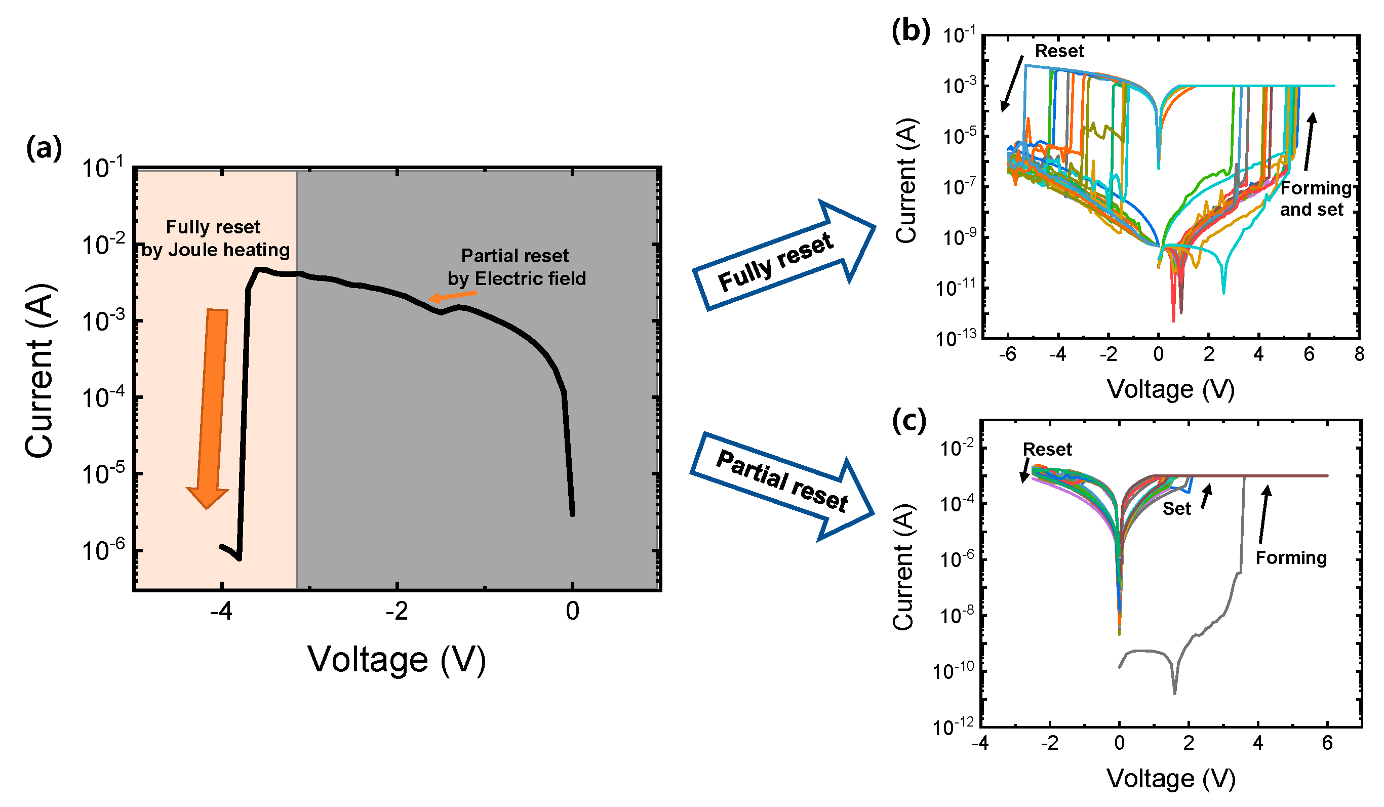
Figure 2a shows the I-V curve of the Cu/HfAlOx/Si device for the reset process after the forming process. It was noted that the partial reset was observed before full reset occurred. It was essential to obtain gradual resistive switching using partial reset. Therefore, we could select the switching mode by initial reset stop voltage. When more than 3.5 V was applied to the device, the current decreased in an abrupt manner. A Cu-based filament formed during the forming process was nearly fully ruptured. The HRS current was a little higher than the initial current level, indicating that there was little remaining of the Cu filament. Figure 2b shows iterative I-V curves for the set and reset processes. The abrupt set and reset were observed during the cycle. Some of the reset process may have dropped sharply into several steps. On the other hand, the gradual set and reset process were obtained after the forming process (Figure 2c). The partial reset that was conducted at a lower reset stop voltage made totally different switching behaviors. The reset process could be dominantly conducted by the electric field. The Cu filament could be ruptured little by little at the beginning of the reset with a negative bias voltage. In both modes, switching did not occur stably for more than 50 endurance cycles. In addition, in order to improve reproducibility and repeatability, Cu ions must be well controlled.
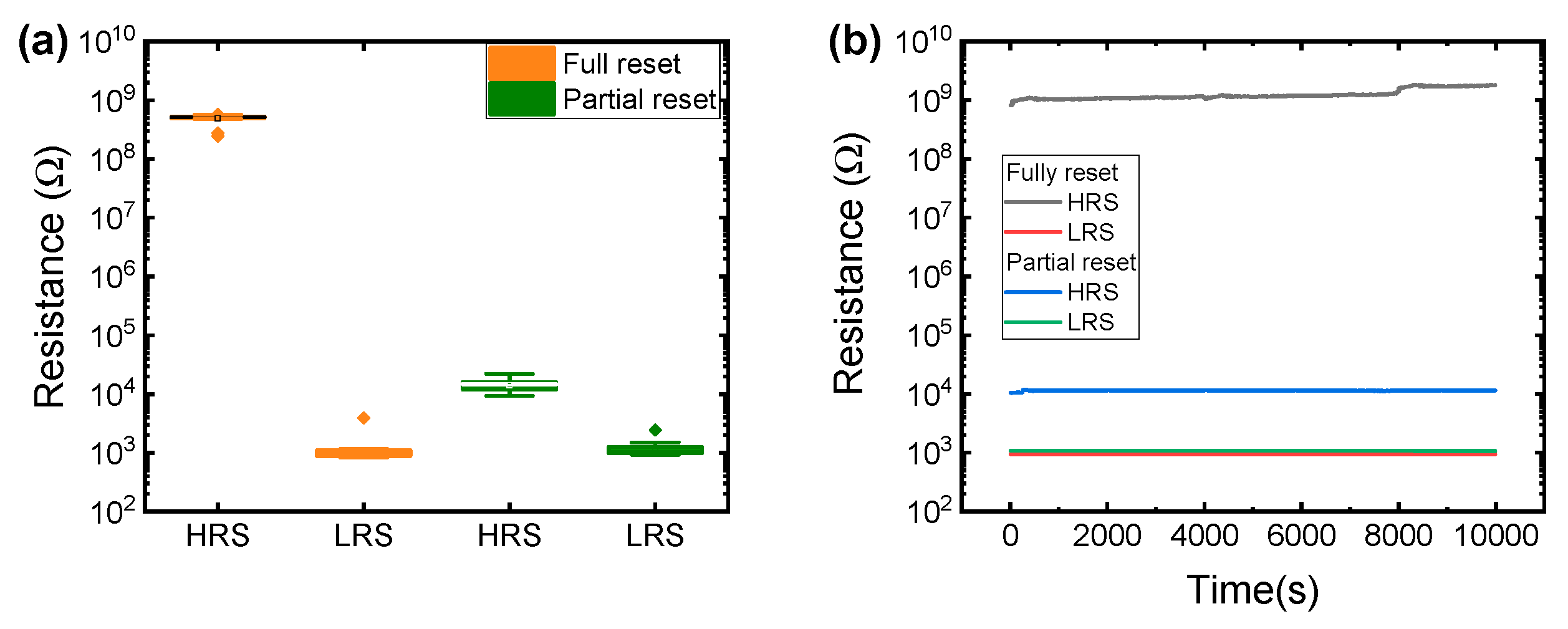
Figure 3a shows the distribution of LRS and HRS in Cu/HfAlOx/Si device in two modes. The average HRS resistances of the full reset mode and the partial reset mode were 491 MΩ and 14.2 kΩ, respectively. Since the full reset mode almost completely ruptured the Cu filament, the HRS resistance was much larger than that of the partial reset mode. Relative standard deviation (RSD) of full reset and partial reset in the HRS were 0.185 and 0.207, which were not very different. The average LRS resistance of full reset and partial reset was 1.12 and 1.17 kΩ, which were nearly same values. This indicates the Cu filaments formed by the set process with the same compliance current were not that different in the two modes. The switching modes could be determined by the reset process. Figure 3b shows the retention test of both switching modes in the LRS and HRS up to 10,000 s. The resistance values were extracted at the read voltage of 0.2 V. The two states were sufficiently distinguishable in both switching modes.
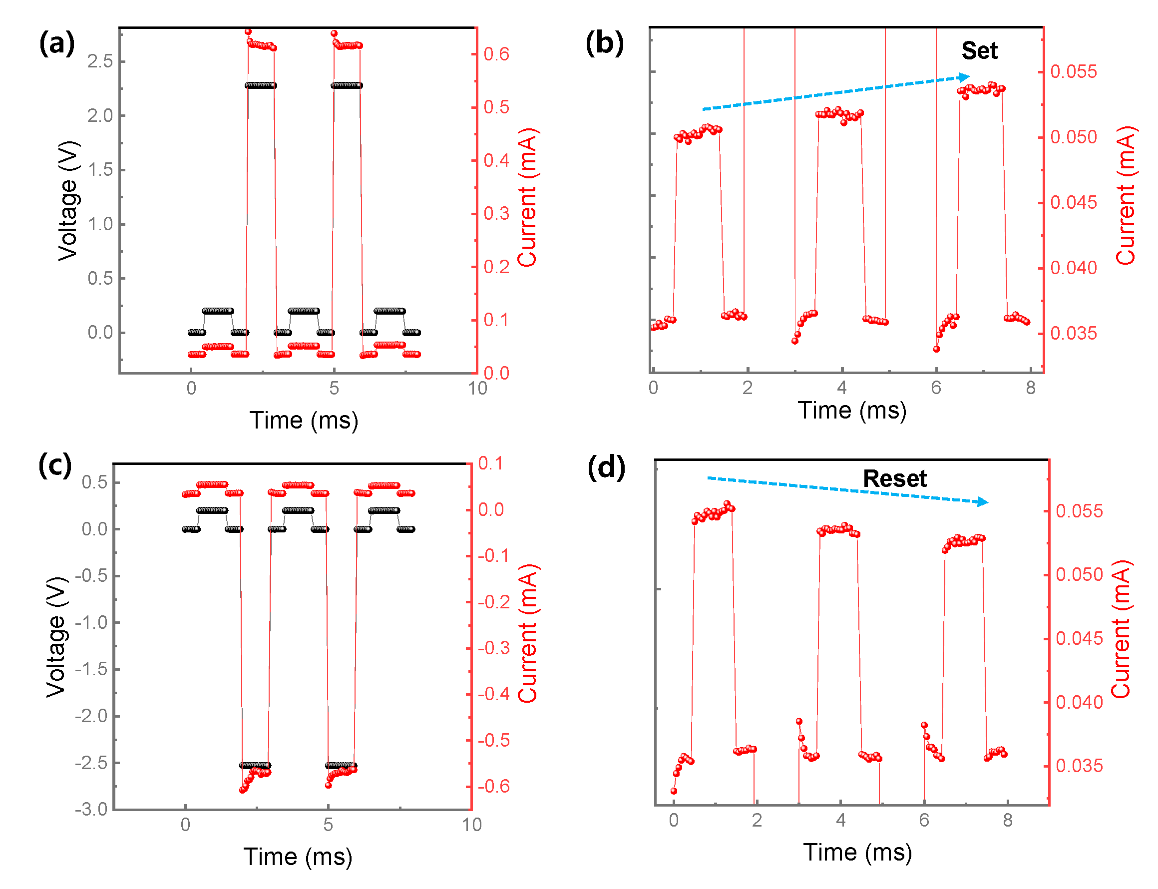
Next, the pulse transient characteristic tests were conducted to implement the synaptic device features for a hardware-based neuromorphic system. In the case of synaptic devices, gradually adjusting the conductance for the applied voltage can improve the performance of the neuromorphic system. Therefore, gradual resistive switching in partial reset switching mode is suitable for synaptic operation. Figure 4a shows the transient characteristics of the set process in partial switching mode. The pulse amplitude and pulse width were 2.3 V and 1 ms for the gradual set process. The read pulses were inserted before and after the set pulse to check the current change. The increase in current was clearly observed in two steps by the read voltage of 0.2 V (Figure 4b). Conversely, the pulses with negative voltage made the decrease in current for the reset process (Figure 4a). Here the pulse voltage and width were −2.55 V and 1 ms, respectively. The current was sensed by read pulses as in the set operation in Figure 4d.
The neuromorphic system is specialized in fields such as pattern recognition. The performance of hardware-based neuromorphic computing can be affected by the RRAM device’s conductance update method. To compare the changes in the conductance of full reset and partial reset cases, the potential and depression characteristics were measured as shown in Figure 5a,b, respectively. The same pulse conditions with set pulse and reset pulse in Figure 4 were used to achieve the potentiation and depression and the conductance was extracted at the read pulse of 0.2 V. After the response with the first pulse, the conductance changed considerably, and from the second pulse, only fluctuation was observed without significant change in the full reset case. This result was similar to the DC sweep mode in which the current increased rapidly at one point as shown in Figure 2b. In depression of full reset mode, the decrease in current was divided into several stages and progresses, but an unstable appearance that increased and decreased again was observed. This may be attributed to the fluctuation of the Cu ions, caused by bias voltage. On the other hand, in the potentiation and depression of partial reset, the conductance changed more gradually. However, there were some variations in the rising and falling of the conductance and the opposite trend was observed by even set pulse. This behavior occurred due to the instability of Cu ions in response to voltage. The dynamic range of the conductance was much smaller compared to the case of the full reset with high on/off ratio [34]. A similar result was reported in the interface type with small on/off ratio and the small dynamic range should be improved to obtain better performance as a neuromorphic device.
Figure 5c shows the neural network for the software-based pattern recognition simulation. The network consists of 784 input layers, 10 output neurons, and synapses fully connecting input neurons and output neurons. In this experiment, since only single cells were fabricated, it was assumed that the weight update of all synapses had the same characteristics as the conductance update of Figure 4a,b. The input neuron received the MINST binary dataset with 28 × 28 pixel images and 10 output neurons classified the 10 classes (numbers) for recognition. Weight values (Wij) were optimized by training to find the right information. A more detailed explanation is available from our past work [35]. Figure 5d shows the recognition rate of full reset and partial reset. For the partial reset, the maximum rate was 71.94% and that of full reset was 61.07%, but the variation was so severe that the minimum rate was down to 10.44%. It should be noted that the partial reset showed a higher and more stable recognition rate. Therefore, the partial reset case was more suitable for the better synaptic property.

4. Conclusions

In summary, the two switching modes were controlled by the reset stop voltage in a Cu/HfAlOx/Si device for neuromorphic application. The material and chemical properties of the alloyed type HfAlOx dielectric were investigated by XPS analysis. Full reset mode accompanied the abrupt set and reset process. On the other hand, the gradual set and reset process was achieved in a partial reset mode with small reset voltage. There was no significant difference between the LRS and HRS variations of the two switching modes. In addition, it was possible to distinguish the on state and off state without significant degradation for 2000 s in the two modes. The gradual increase and decrease in the current was confirmed in the transient characteristics. Finally, we demonstrated the potentiation and depression curves by partial reset was more suitable for a synaptic device than by full reset.

Author Contributions

S.K. (Seunghyun Kim) conducted the electrical measurements and wrote the manuscript; O.K. and H.R. conducted the simulation work. S.K. (Sungjun Kim) designed the experiment and supervised the study. All authors have read and agreed to the published version of the manuscript.

Funding

This work was supported in part by the National Research Foundation of Korea (NRF), grant funded by the Korean government (MSIP), under Grant 2021R1C1C1004422.

Institutional Review Board Statement

Not applicable.

Informed Consent Statement

Not applicable.

Data Availability Statement

Not applicable.

Conflicts of Interest

The authors declare no conflict of interest.

References

  1. Sim, J.-M.; Kang, M.; Song, Y.-H. A New Read Scheme for Alleviating Cell-to-Cell Interference in Scaled-Down 3D NAND Flash Memory. Electronics 2020, 9, 1775. [Google Scholar] [CrossRef]
  2. Park, J. Neuromorphic Computing Using Emerging Synaptic Devices: A Retrospective Summary and an Outlook. Electronics 2020, 9, 1414. [Google Scholar] [CrossRef]
  3. Wu, M.; Ting, Y.; Chen, J.; Wu, W. Low Power Consumption Nanofilamentary ECM and VCM Cells in a Single Sidewall of High-Density VRRAM Arrays. Adv. Sci. 2019, 6, 1902363. [Google Scholar] [CrossRef]
  4. Shen, Z.; Zhao, C.; Qi, Y.; Xu, W.; Liu, Y.; Mitrovic, I.Z.; Yang, L.; Zhao, C. Advances of RRAM Devices: Resistive Switching Mechanisms, Materials and Bionic Synaptic Application. Nanomaterials 2020, 10, 1437. [Google Scholar] [CrossRef]
  5. Banerjee, W. Challenges and Applications of Emerging Nonvolatile Memory Devices. Electronics 2020, 9, 1029. [Google Scholar] [CrossRef]
  6. Lanza, M.; Wong, H.-S.P.; Pop, E.; Ielmini, D.; Strukov, D.; Regan, B.C.; Larcher, L.; Villena, M.A.; Yang, J.J.; Goux, L.; et al. Recommended Methods to Study Resistive Switching Devices. Adv. Electron. Mater. 2019, 5, 1800143. [Google Scholar] [CrossRef] [Green Version]
  7. Pan, F.; Gao, S.; Chen, C.; Song, C.; Zeng, F. Recent progress in resistive random access memories: Materials, switching mechanisms, and performance. Mater. Sci. Eng. R: Rep. 2014, 83, 1–59. [Google Scholar] [CrossRef]
  8. Lin, J.; Wang, S.; Liu, H. Multi-Level Switching of Al-Doped HfO2 RRAM with a Single Voltage Amplitude Set Pulse. Electronics 2021, 10, 731. [Google Scholar] [CrossRef]
  9. Pérez, E.; Ossorio, Ó.G.; Dueñas, S.; Castán, H.; García, H.; Wenger, C. Programming Pulse Width Assessment for Reliable and Low-Energy Endurance Performance in Al:HfO2-Based RRAM Arrays. Electronics 2020, 9, 864. [Google Scholar] [CrossRef]
  10. Ryu, H.; Choi, J.; Kim, S. Voltage Amplitude-Controlled Synaptic Plasticity from Complementary Resistive Switching in Alloying HfOx with AlOx-Based RRAM. Metals 2020, 10, 1410. [Google Scholar] [CrossRef]
  11. Mikhaylov, A.; Belov, A.; Korolev, D.; Antonov, I.; Kotomina, V.; Kotina, A.; Gryaznov, E.; Sharapov, A.; Koryazhkina, M.; Kryukov, R.; et al. Multilayer Metal-Oxide Memristive Device with Stabilized Resistive Switching. Adv. Mater. Technol. 2020, 5, 1900607. [Google Scholar] [CrossRef]
  12. Ryu, H.; Kim, S. Self-Rectifying Resistive Switching and Short-Term Memory Characteristics in Pt/HfO2/TaOx/TiN Artificial Synaptic Device. Nanomaterials 2020, 10, 2159. [Google Scholar] [CrossRef]
  13. Ryu., H.; Kim, S. Pseudo-Interface Switching of a Two-Terminal TaOx/HfO2 Synaptic Device for Neuromorphic Applications. Nanomaterials 2020, 10, 1550. [Google Scholar] [CrossRef] [PubMed]
  14. Kim, S.; Chen, J.; Chen, Y.-C.; Kim, M.-H.; Kim, H.; Kwon, M.-W.; Hwang, S.; Ismail, M.; Li, Y.; Miao, X.-S.; et al. Neuronal dynamics in HfO x/AlOy-based homeothermic synaptic memristors with low-power and homogeneous resistive switching. Nanoscale 2019, 11, 237–245. [Google Scholar] [CrossRef] [Green Version]
  15. Kim, T.-H.; Nili, H.; Kim, M.-H.; Min, K.K.; Park, B.-G.; Kim, H. Reset-voltage-dependent precise tuning operation of TiOx/Al2O3 memristive crossbar array. Appl. Phys. Lett. 2020, 117, 152103. [Google Scholar] [CrossRef]
  16. Waser, R.; Dittmann, R.; Staikov, G.; Szot, K. Redox-Based Resistive Switching Memories - Nanoionic Mechanisms, Prospects, and Challenges. Adv. Mater. 2009, 21, 2632–2663. [Google Scholar] [CrossRef]
  17. Laurlia, T.; Zeng, K.; Kivilahti, J. Failure mechanism of Ta diffusion abrrier between Cu and Si. J. Appl. Phys. 2000, 88, 3377. [Google Scholar] [CrossRef]
  18. Son, J.Y.; Shin, Y.-H. Direct observation of conducting filaments on resistive switching of NiO thin films. Appl. Phys. Lett. 2008, 92, 222106. [Google Scholar] [CrossRef]
  19. Schroeder, H.; Jeong, D.S. Resistive switching in a Pt/TiO2/Pt thin film stack–a candidate for a non-volatile ReRAM. Microelectron. Eng. 2007, 84, 1982. [Google Scholar] [CrossRef]
  20. Simanjuntak, F.M.; Ohno, T.; Chandrasekaran, C.; Tseng, T.Y.; Samukawa, S. Neutral oxygen irradiation enhanced forming-less ZnO-based transparent analog memristor devices for neuromorphic computing applications. Nanotechnology 2020, 31, 26LT01. [Google Scholar] [CrossRef] [PubMed]
  21. Carlos, E.; Branquinho, R.; Martins, R.; Kiazadeh, A.; Fortunato, E. Recent Progress in Solution-Based Metal Oxide Resistive Switching Devices. Adv. Mater. 2021, 33, e2004328. [Google Scholar] [CrossRef]
  22. Simanjuntak, F.M.; Ohno, T.; Samukawa, S. Film-Nanostructure-Controlled Inerasable-to-Erasable Switching Transition in ZnO-Based Transparent Memristor Devices: Sputtering-Pressure Dependency. ACS Appl. Electron. Mater. 2019, 11, 2184–2189. [Google Scholar] [CrossRef]
  23. Ryu, H.; Kim, S. Synaptic Characteristics from Homogeneous Resistive Switching in Pt/Al2O3/TiN Stack. Nanomaterials 2020, 10, 2055. [Google Scholar] [CrossRef]
  24. Simanjuntak, F.M.; Ohno, T.; Samukawa, S. Neutral Oxygen Beam Treated ZnO-Based Resistive Switching Memory Device. ACS Appl. Electron. Mater. 2019, 1, 18–24. [Google Scholar] [CrossRef]
  25. Ryu, H.; Kim, S. Gradually Tunable Conductance in TiO2/Al2O3 Bilayer Resistors for Synaptic Device. Metals 2021, 11, 440. [Google Scholar] [CrossRef]
  26. Simanjuntak, F.M.; Chandrasekaran, S.; Lin, C.-C.; Tseng, T.-Y. Switching Failure Mechanism in Zinc Peroxide-Based Programmable Metallization Cell. Nanoscale Res. Lett. 2018, 13, 1–8. [Google Scholar] [CrossRef] [PubMed]
  27. Ryu, H.; Kim, S. Irregular Resistive Switching Behaviors of Al2O3-Based Resistor with Cu Electrode. Metals 2021, 11, 653. [Google Scholar] [CrossRef]
  28. Chan, A. Memory selector devices and crossbar array design: A modeling-based assessment. J. Comput. Electron. 2017, 16, 1186–1200. [Google Scholar] [CrossRef]
  29. Mahata, C.; Kim, S. Modified resistive switching performance by increasing Al concentration in HfO2 on transparent indium tin oxide electrode. Ceram. Int. 2021, 47, 1199–1207. [Google Scholar] [CrossRef]
  30. Sokolov, A.; Som, S.K.; Han, H.H.; Jeon, Y.R.; Lee, J.H.; Choi, C. Comparative study of Al2O3, HfO2, and HfAlOx for improved self-compliance bipolar resistive switching. J. Am. Ceram. Soc. 2017, 100, 5638–5648. [Google Scholar] [CrossRef]
  31. Tien, T.-C.; Lin, L.-C.; Lee, L.-S.; Hwang, C.-J.; Maikap, S.; Shulga, Y.M. Analysis of weakly bonded oxygen in HfO2/SiO2/Si stacks by using HRBS and ARXPS. J. Mater. Sci. Mater. Electron. 2010, 21, 475–480. [Google Scholar] [CrossRef]
  32. Kumar, K.; Biswas, K. Cryomilling: An environment friendly approach of preparation large quantity ultra refined pure aluminium nanoparticles. J. Mater. Res. Technol. 2019, 8, 63–74. [Google Scholar] [CrossRef]
  33. Rahman, M.; Kim, J.-G.; Kim, D.-H.; Kim, T.-W. Characterization of Al Incorporation into HfO2 Dielectric by Atomic Layer Deposition. Micromachines 2019, 10, 361. [Google Scholar] [CrossRef] [Green Version]
  34. Cho, H.; Kim, S. Short-Term Memory Dynamics of TiN/Ti/TiO2/SiOx/Si Resistive Random Access Memory. Nanomaterials 2020, 10, 1821. [Google Scholar] [CrossRef] [PubMed]
  35. Ryu, J.-H.; Kim, B.; Hussain, F.; Mahata, C.; Ismail, M.; Kim, Y.; Kim, S. Bio-inspired synaptic functions from a transparent zinc-tin-oxide-based memristor for neuromorphic engineering. Appl. Surf. Sci. 2021, 544, 148796. [Google Scholar] [CrossRef]
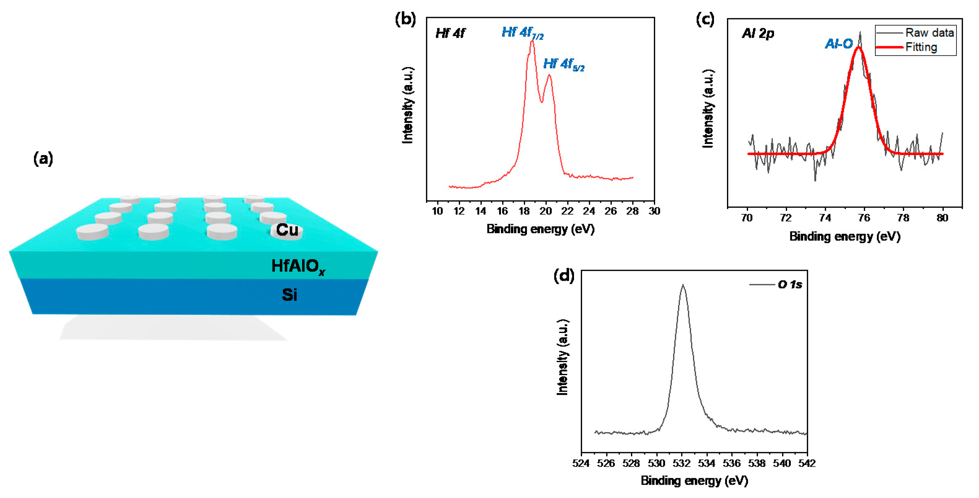
Figure 1. (a) Schematic of Cu/HfAlOx/Si device. (b) Hf 4f, (c) Al 2p and (d) O 1s spectra of HfAlOx film.
Metals 11 00772 g001
Figure 2. (a) Switching decision by reset voltage amplitude. I-V curves by (b) full reset mode and (c) partial reset mode.
Metals 11 00772 g002
Figure 3. (a) HRS and LRS resistance distribution and (b) retention for full reset mode and partial reset mode for 10,000 s.
Metals 11 00772 g003
Figure 4. (a) Transient characteristics and (b) current part is expanded by set pulses. (c) Transient characteristics and (d) current part is expanded by reset pulses.
Metals 11 00772 g004
Figure 5. Potentiation and depression characteristics for (a) full reset mode and (b) partial reset mode. (c) Neural network for neuromorphic simulation. (d) Pattern recognition accuracy when using full reset mode and partial reset mode as synaptic weight in neural network.
Metals 11 00772 g005
Publisher’s Note: MDPI stays neutral with regard to jurisdictional claims in published maps and institutional affiliations.