Effects of Oxygen Precursor on Resistive Switching Properties of CMOS Compatible HfO2-Based RRAM

Abstract
:1. Introduction
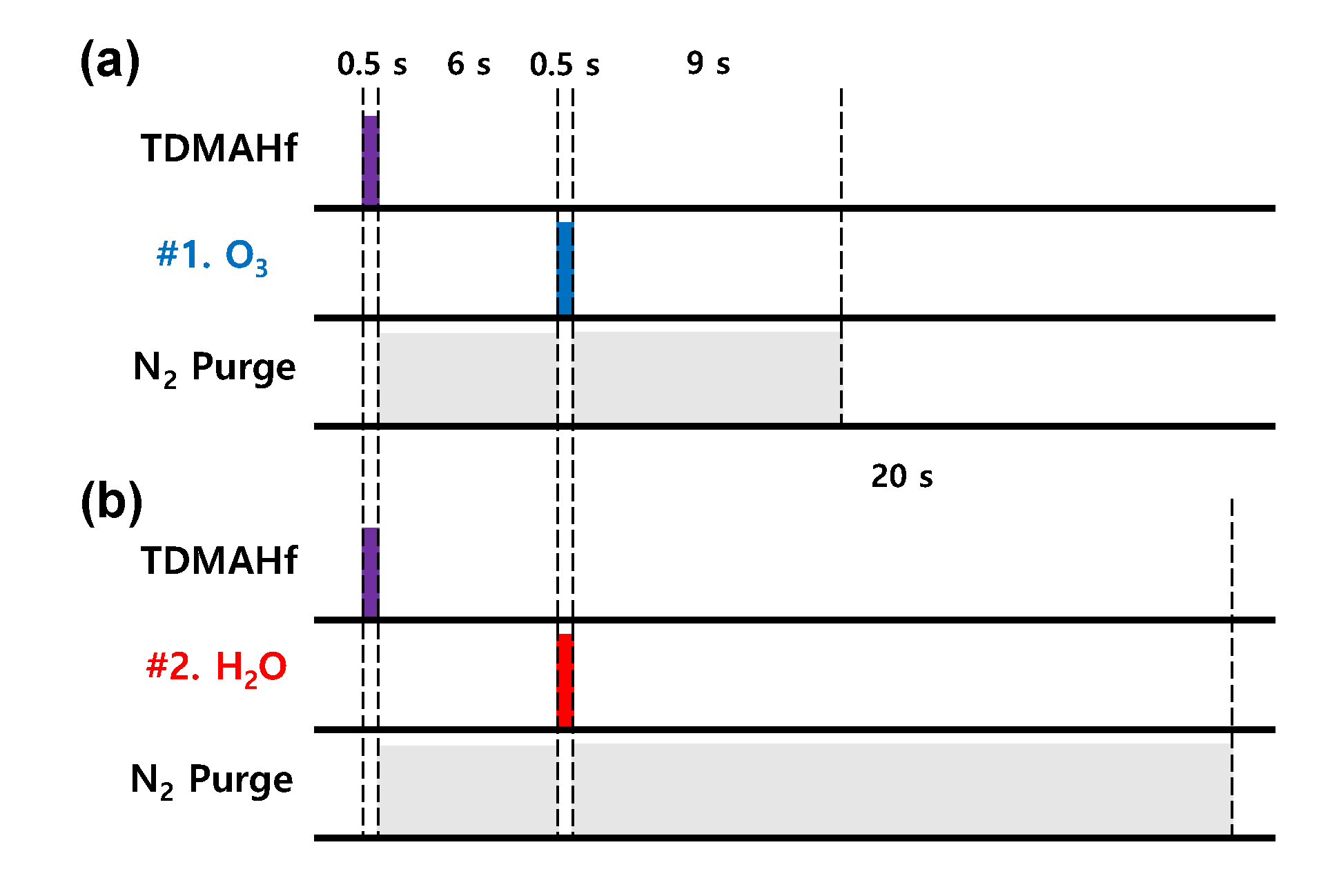
2. Materials and Methods
3. Results and Discussion
4. Conclusions
Supplementary Materials
Author Contributions
Funding
Institutional Review Board Statement
Informed Consent Statement
Data Availability Statement
Conflicts of Interest
References
- Lanza, M.; Wong, H.-S.P.; Pop, E.; Ielmini, D.; Strukov, D.; Regan, B.C.; Larcher, L.; Villena, M.A.; Yang, J.J.; Goux, L.; et al. Recommended Methods to Study Resistive Switching Devices. Adv. Electron. Mater. 2018, 5, 1800143. [Google Scholar] [CrossRef] [Green Version]
- Pan, F.; Gao, S.; Chen, C.; Song, C.; Zeng, F. Recent progress in resistive random access memories: Materials, switching mechanisms, and performance. Mater. Sci. Eng. R Rep. 2014, 83, 1–59. [Google Scholar] [CrossRef]
- Waser, R.; Dittmann, R.; Staikov, G.; Szot, K. Redox-Based Resistive Switching Memories—Nanoionic Mechanisms, Prospects, and Challenges. Adv. Mater. 2009, 21, 2632–2663. [Google Scholar] [CrossRef]
- Shen, Z.; Zhao, C.; Qi, Y.; Xu, W.; Liu, Y.; Mitrovic, I.Z.; Yang, L.; Zhao, C. Advances of RRAM Devices: Resistive Switching Mechanisms, Materials and Bionic Synaptic Application. Nanomaterials 2020, 10, 1437. [Google Scholar] [CrossRef] [PubMed]
- Fong, S.W.; Neumann, C.M.; Wong, H.S.P. Phase-Change Memory—Towards a Storage-Class Memory. IEEE Trans. Electron Devices 2017, 64, 4374–4385. [Google Scholar] [CrossRef]
- Zhao, W.S.; Zhang, Y.; Devolder, Y.; Klein, J.O.; Ravelosona, D.; Chappert, C.; Mazoyer, P. Failure and reliability analysis of STT-MRAM. Microelectron. Reliab. 2012, 52, 1848–1852. [Google Scholar] [CrossRef]
- Wu, M.C.; Lin, Y.-W.; Jang, W.-Y.; Lin, C.-H.; Tseng, T.-Y. Low-power and highly reliable multilevel operation in ZrO2 1T1R RRAM. IEEE Electron Device Lett. 2011, 32, 1026–1028. [Google Scholar] [CrossRef]
- Su, T.-H.; Lee, K.-J.; Wang, L.-W.; Chang, Y.-C.; Wang, Y.-H. Resistive Switching Behavior of Magnesium Zirconia Nickel Nanorods. Materials 2020, 13, 2755. [Google Scholar] [CrossRef] [PubMed]
- Ryu, H.; Kim, S. Irregular Resistive Switching Behaviors of Al2O3-Based Resistor with Cu Electrode. Metals 2021, 11, 653. [Google Scholar] [CrossRef]
- Ryu, H.; Kim, S. Gradually Modified Conductance in the Self-Compliance Region of an Atomic-Layer-Deposited Pt/TiO2/HfAlOx/TiN RRAM Device. Metals 2021, 11, 1199. [Google Scholar] [CrossRef]
- Maikap, S.; Banergee, W. In Quest of Nonfilamentary Switching: A Synergistic Approach of Dual Nanostructure Engineering to Improve the Variability and Reliability of Resistive Random-Access-Memory Devices. Adv. Electron. Mater. 2020, 6, 2000209. [Google Scholar] [CrossRef]
- Choi, J.; Kim, S. Nonlinear Characteristics of Complementary Resistive Switching in HfAlOx-Based Memristor for High-Density Cross-Point Array Structure. Coatings 2020, 10, 765. [Google Scholar] [CrossRef]
- Pérez, E.; Ossorio, Ó.G.; Dueñas, S.; Castán, H.; García, H.; Wenger, C. Programming Pulse Width Assessment for Reliable and Low-Energy Endurance Performance in Al:HfO2-Based RRAM Arrays. Electronics 2020, 9, 864. [Google Scholar] [CrossRef]
- Mikhaylov, A.; Belov, A.; Korolev, D.; Antonov, I.; Kotomina, V.; Kotina, A.; Gryaznov, E.; Sharapov, A.; Koryazhkina, M.; Kryukov, R.; et al. Multilayer Metal-Oxide Memristive Device with Stabilized Resistive Switching. Adv. Mater. Technol. 2020, 5, 1900607. [Google Scholar] [CrossRef]
- Ismail, M.; Kim, S. Negative differential resistance effect and dual resistive switching properties in a transparent Ce-based devices with opposite forming polarity. Appl. Surf. Sci. 2020, 530, 147284. [Google Scholar] [CrossRef]
- Peng, C.S.; Chang, W.Y.; Lin, M.H.; Chen, W.S.; Chen, F.; Tsai, M.J. Polarity Reversion of the Operation Mode of HfO2-Based Resistive Random Access Memory Devices by Inserting Hf Metal Layer. J. Nanosci. Nanotechnol. 2013, 13, 1733–1737. [Google Scholar] [CrossRef] [PubMed] [Green Version]
- Prakash, A.; Jana, D.; Maikap, S. TaOx-based resistive switching memories: Prospective and challenges. Nanoscale Res. Lett. 2013, 8, 418. [Google Scholar] [CrossRef] [PubMed] [Green Version]
- Yang, J.; Ryu, H.; Kim, S. Resistive and synaptic properties modulation by electroforming polarity in CMOS-compatible Cu/HfO2/Si device. Chaos Solitons Fractals 2021, 145, 110783. [Google Scholar] [CrossRef]
- Ryu, H.; Kim, S. Gradually Tunable Conductance in TiO2/Al2O3 Bilayer Resistors for Synaptic Device. Metals 2021, 11, 440. [Google Scholar] [CrossRef]
- Ryu, H.; Kim, S. Self-Rectifying Resistive Switching and Short-Term Memory Characteristics in Pt/HfO2/TaOx/TiN Artificial Synaptic Device. Nanomaterials 2020, 10, 2159. [Google Scholar] [CrossRef] [PubMed]
- Ielmini, D.; Wong, H.-S.P. In-memory computing with resistive switching devices. Nat. Electron. 2018, 1, 333–343. [Google Scholar] [CrossRef]
- Yang, J.J.; Strukov, D.B.; Stewart, D.R. Memristive devices for computing. Nat. Nanotechnol. 2013, 8, 13–24. [Google Scholar] [CrossRef] [PubMed]
- Jo, S.H.; Chang, T.; Ebong, I.; Bhadviya, B.B.; Mazumder, P.; Lu, W. Nanoscale memristor device as synapse in neuromorphic. Nano Lett. 2010, 10, 1297–1301. [Google Scholar] [CrossRef] [PubMed]
- Cho, H.; Kim, S. Short-Term Memory Dynamics of TiN/Ti/TiO2/SiOx/Si Resistive Random Access Memory. Nanomaterials 2020, 10, 1821. [Google Scholar] [CrossRef]
- Cho, H.; Kim, S. Emulation of Biological Synapse Characteristics from Cu/AlN/TiN Conductive Bridge Random Access Memory. Nanomaterials 2020, 10, 1709. [Google Scholar] [CrossRef] [PubMed]
- Mikhaylov, A.; Pimashkim, A.; Pigareva, Y.; Gerasimova, S.; Gryaznov, E.; Shchanikov, S.; Zuev, A.; Talanov, M.; Lavrov, I.; Demin, V.; et al. Neurohybrid memristive CMOS-integrated systems for biosensors and neuroprosthetics. Front. Neurosci. 2020, 14, 358. [Google Scholar] [CrossRef]
- Surazhevsky, I.A.; Demin, V.A.; IIlyasov, A.L.; Emelyanov, A.V.; Nikiruy, K.E.; Rylkov, V.V.; Shchanikov, S.; Bordanov, I.; Gerasimova, S.A.; Guseinov, D.; et al. Noise-assisted persistence and recovery of memory state in a memristive spiking neuromorphic network. Chaos Solitons Fractals 2020, 146, 110890. [Google Scholar] [CrossRef]
- Cho, H.; Kim, S. Enhancing Short-Term Plasticity by Inserting a Thin TiO2 Layer in WOx-Based Resistive Switching Memory. Coatings 2020, 10, 908. [Google Scholar] [CrossRef]
- Ryu, H.; Choi, J.; Kim, S. Voltage Amplitude-Controlled Synaptic Plasticity from Complementary Resistive Switching in Alloying HfOx with AlOx-Based RRAM. Metals 2020, 10, 1410. [Google Scholar] [CrossRef]
- Ryu, H.; Kim, S. Pseudo-Interface Switching of a Two-Terminal TaOx/HfO2 Synaptic Device for Neuromorphic Applications. Nanomaterials 2020, 10, 1550. [Google Scholar] [CrossRef]
- Kim, T.H.; Nili, H.; Kim, M.H.; Min, K.K.; Park, B.G.; Kim, H. Reset-voltage-dependent precise tuning operation of TiOx/Al2O3 memristive crossbar array. Appl. Phys. Lett. 2020, 117, 152103. [Google Scholar] [CrossRef]
- Ryu, H.; Kim, S. Volatile Resistive Switching Characteristics of Pt/HfO2/TaOx/TiN Short-Term Memory Device. Metals 2021, 11, 1207. [Google Scholar] [CrossRef]
- Ryu, H.; Kim, S. Implementation of a reservoir computing system using the short-term effects of Pt/HfO2/TaOx/TiN memristors with self-rectification. Chaos Solitons Fractals 2021, 150, 111223. [Google Scholar] [CrossRef]
- Wang, I.T.; Chang, C.C.; Chiu, L.W.; Chou, T.; Hou, T.H. 3D Ta/TaOx/TiO2/Ti synaptic array and linearity tuning of weight update for hardware neural network applications. Nanotechnology 2016, 27, 365204. [Google Scholar] [CrossRef] [PubMed] [Green Version]
- Park, J.; Ryu, H.; Kim, S. Nonideal resistive and synaptic characteristics in Ag/ZnO/TiN device for neuromorphic system. Sci. Rep. 2021, 11, 16601. [Google Scholar] [CrossRef] [PubMed]
- Hwang, H.-G.; Woo, J.-U.; Lee, T.-H.; Park, S.M.; Lee, T.-G.; Lee, W.H.; Nahm, S. Synaptic plasticity and preliminary-spike-enhanced plasticity in a CMOS-compatible Ta2O5 memristor. Mater. Des. 2020, 187, 108400. [Google Scholar] [CrossRef]
- Padovani, A.; Woo, J.; Hwang, H.; Larcher, L. Understanding and Optimization of Pulsed SET Operation in HfOx-Based RRAM Devices for Neuromorphic Computing Applications. IEEE Electron Device Lett. 2018, 39, 672–675. [Google Scholar] [CrossRef]
- Zhang, W.; Gao, B.; Tang, J.; Li, X.; Wu, W.; Qian, H.; Wu, H. Analog-Type Resistive Switching Devices for Neuromorphic Computing. Phys. Status Solidi—Rapid Res. Lett. 2019, 13, 1900204. [Google Scholar] [CrossRef]
- Zhao, M.; Gao, B.; Tang, J.; Qian, H.; Wu, H. Reliability of analog resistive switching memory for neuromorphic computing. Appl. Phys. Rev. 2020, 7, 011301. [Google Scholar] [CrossRef]
- Emelyanov, A.V.; Nikiruy, K.E.; Serenko, A.V.; Sitnikov, A.V.; Presnyakov, M.Y.; Rybka, R.B.; Sboev, A.G.; Rylkov, V.V.; Kashkarov, P.K.; Kovalchuk, M.V.; et al. Self-adaptive STDP-based learning of a spiking neuron with nanocomposite memristive weights. Nanotechnology 2020, 31, 045201. [Google Scholar] [CrossRef]
- Lee, M.J.; Lee, C.B.; Lee, D.; Lee, S.R.; Chang, M.; Hur, J.H.; Kim, Y.-B.; Kim, C.-J.; Seo, D.H.; Chung, U.-I.; et al. A fast, high endurance and scalable non-volatile memory device made from asymmetric Ta2O5-x/TaO2-x bilayer structures. Nat. Mater. 2011, 10, 625–630. [Google Scholar] [CrossRef] [PubMed]
- Wang, Y.; Liu, Q.; Long, S.B.; Wang, W.; Wang, Q.; Zhang, M.H.; Zhang, S.; Li, Y.; Zuo, Q.; Yang, J.; et al. Investigation of resistive switching in Cu-doped HfO2 thin film for multilevel non-volatile memory applications. Nanotechnology 2010, 21, 045202. [Google Scholar] [CrossRef]
- Chen, L.; He, Z.-Y.; Wang, T.-Y.; Dai, Y.-W.; Zhu, H.; Sun, Q.-Q.; Zhang, D.W. CMOS Compatible Bio-Realistic Implementation with Ag/HfO2-Based Synaptic Nanoelectronics for Artificial Neuromorphic System. Electronics 2018, 7, 80. [Google Scholar] [CrossRef] [Green Version]
- Lin, J.; Wang, S.; Liu, H. Multi-Level Switching of Al-Doped HfO2 RRAM with a Single Voltage Amplitude Set Pulse. Electronics 2021, 10, 731. [Google Scholar] [CrossRef]
- Ryu, H.; Kim, S. Improved Pulse-Controlled Conductance Adjustment in Trilayer Resistors by Suppressing Current Overshoot. Nanomaterials 2020, 10, 2462. [Google Scholar] [CrossRef]
- Liu, C.-F.; Tang, X.-G.; Wang, L.-Q.; Tang, H.; Jiang, Y.-P.; Liu, Q.-X.; Li, W.-H.; Tang, Z.-H. Resistive Switching Characteristics of HfO2 Thin Films on Mica Substrates Prepared by Sol-Gel Process. Nanomaterials 2019, 9, 1124. [Google Scholar] [CrossRef] [Green Version]
- George, S.M. Atomic Layer Deposition: An Overview. Chem. Rev. 2016, 110, 111–131. [Google Scholar] [CrossRef]
- Liu, J.; Koide, Y. An Overview of High-k Oxides on Hydrogenated-Diamond for Metal-Oxide-Semiconductor Capacitors and Field-Effect Transistors. Sensors 2018, 18, 1813. [Google Scholar] [CrossRef] [Green Version]
- Kim, S.; Kwon, O.; Ryu, H.; Kim, S. Improved Synaptic Device Properties of HfAlOx Dielectric on Highly Doped Silicon Substrate by Partial Reset Process. Metals 2021, 11, 772. [Google Scholar] [CrossRef]
- Mahata, C.; Kim, S. Modified resistive switching performance by increasing Al concentration in HfO2 on transparent indium tin oxide electrode. Ceram. Int. 2021, 47, 1199–1207. [Google Scholar] [CrossRef]
- Bai, Y.; Wu, H.; Wu, R.; Zhang, Y.; Deng, N.; Yu, Z.; Qian, H. Study of Multi-level Characteristics for 3D Vertical Resistive Switching Memory. Sci. Rep. 2014, 4, 5780. [Google Scholar] [CrossRef] [PubMed] [Green Version]
- Lapteva, M.; Beladiya, V.; Riese, S.; Hanke, P.; Otto, F.; Fritz, T.; Schmitt, P.; Stenzel, O.; Tünnermann, A.; Szeghalmi, A. Influence of temperature and plasma parameters on the properties of PEALD HfO2. Opt. Mater. Express 2021, 11, 1918–1942. [Google Scholar] [CrossRef]
- Grossi, A.; Perez, E.; Zambelli, C.; Olivo, P.; Miranda, E.; Roelofs, R.; Woodruff, J.; Raisanen, P.; Li, W.; Givens, M.; et al. Impact of the precursor chemistry and process conditions on the cell-to-cell variability in 1T-1R based HfO2 RRAM devices. Sci. Rep. 2018, 8, 11160. [Google Scholar] [CrossRef] [PubMed] [Green Version]
- Zazpe, R.; Ungureanu, M.; Golmar, F.; Stoliar, P.; Llopis, R.; Casanova, F.; Pickip, D.; Rogero, C.; Hueso, L.E. Resistive switching dependence on atomic layer deposition parameters in HfO2-based memory devices. J. Mater. Chem. C 2014, 2, 3204–3211. [Google Scholar] [CrossRef]
- Sokolov, A.S.; Jeon, Y.R.; Kim, S. Influence of oxygen vacancies in ALD HfO2-x thin films on non-volatile resistive switching phenomena with a Ti/HfO2-x/Pt structure. Appl. Surf. Sci. 2018, 434, 822–830. [Google Scholar] [CrossRef]
- Chandrasekaran, S.; Simanjuntak, F.M.; Saminatha, R.; Panda, D.; Tseng, T.Y. Improving linearity by introducing Al in HfO2 as a memristor synapse device. Nanotechnology 2019, 30, 445205. [Google Scholar] [CrossRef]
- Won, S.; Lee, S.Y.; Park, J.; Seo, H. Forming-less and Non-Volatile Resistive Switching in WOX by Oxygen Vacancy Control at Interfaces. Sci. Rep. 2017, 7, 10186. [Google Scholar] [CrossRef] [Green Version]
- Cheng, Y.L.; Chang, Y.L.; Hsieh, C.Y.; Lin, J.R. Comprehensive comparison of structural, electrical, and reliability characteristics of HfO2 gate dielectric with H2O or O3 oxidant. J. Vac. Sci. Technol. A 2013, 31, 01A141. [Google Scholar] [CrossRef]
- Lee, S.Y.; Kim, H.K.; Lee, J.H.; Yu, I.H.; Lee, J.H.; Hwang, C.S. Effects of O3 and H2O as oxygen sources on the atomic layer deposition of HfO2 gate dielectrics at different deposition temperatures. J. Mater. Chem. C 2014, 2, 2558. [Google Scholar] [CrossRef]
- Blachke, D.; Munnik, F.; Grenzer, J.; Rebohle, L.; Schmidt, H.; Zahn, P.; Gemming, S. A correlation study of layer growth rate, thickness uniformity, stoichiometry, and hydrogen impurity level in HfO2 thin films grown by ALD between 100 C and 350 C. Appl. Surf. Sci. 2020, 506, 144188. [Google Scholar] [CrossRef]
- Park, I.S.; Lee, J.; Yoon, S.; Chung, K.J.; Lee, S.; Park, J.; Kim, C.K.; Ahn, J. Oxidant Effect on Resistance Switching Characteristics of HfO2 film Grown Atomic Layer Deposition. ECS Trans. 2007, 11, 61–67. [Google Scholar] [CrossRef]


Publisher’s Note: MDPI stays neutral with regard to jurisdictional claims in published maps and institutional affiliations. |
© 2021 by the authors. Licensee MDPI, Basel, Switzerland. This article is an open access article distributed under the terms and conditions of the Creative Commons Attribution (CC BY) license (https://creativecommons.org/licenses/by/4.0/).
Share and Cite
Ryu, H.; Kim, S. Effects of Oxygen Precursor on Resistive Switching Properties of CMOS Compatible HfO2-Based RRAM. Metals 2021, 11, 1350. https://doi.org/10.3390/met11091350
Ryu H, Kim S. Effects of Oxygen Precursor on Resistive Switching Properties of CMOS Compatible HfO2-Based RRAM. Metals. 2021; 11(9):1350. https://doi.org/10.3390/met11091350
Chicago/Turabian StyleRyu, Hojeong, and Sungjun Kim. 2021. "Effects of Oxygen Precursor on Resistive Switching Properties of CMOS Compatible HfO2-Based RRAM" Metals 11, no. 9: 1350. https://doi.org/10.3390/met11091350