Abstract
In this experiment, a Sn35Bi0.3Ag–xIn (x = 0, 0.5, 1.0, 1.5) alloy solder was prepared by electromagnetic induction heating furnace. The effects of In on the thermodynamic properties, wettability, interface microstructure, and soldering performance of Sn35Bi0.3Ag–xIn/Cu solder joints were studied by a synchrotron thermal analyzer (DSC), contact-angle measuring instrument, scanning electron microscope (SEM), energy dispersive spectrometer (EDS), and universal tensile testing machine. The research showed that adding a small amount of In reduced the solid–liquid temperature and improved the wettability of the alloy solder. At the interface of SnBiAg–xIn/Cu joint, it was found that In atoms replaced part of Sn atoms, forming the Cu6 (Sn, In)5 phase and scallop-like Cu3 (Sn, In) phase. When adding 0.5% and 1.0% In elements, it was found that the Bi phase appeared on the solder side of the interface layer, which hindered the growth of the intermetallic compound (IMC) and reduced the thickness of the IMC layer. Among them, the thickness of the IMC layer of the SnBiAg–1.0In/Cu joint was the smallest, and the shear strength was the highest, which was 55.1 MPa. In addition, the fracture morphology of the solder joint was observed, and it was found that the fracture mode was brittle fracture, and the SnBiAg–xIn/Cu solder joint fractured from the IMC and solder side.
1. Introduction
With the rapid development of the electronics industry, multifunctionality and miniaturization have become the main trends in the development of electronic devices today. Therefore, the requirements of the electronic packaging components for solder joints are becoming higher and higher, and the size of solder joints is becoming smaller and smaller [1]. In this context, low-melting-point circuit interconnection materials have become a hot research topic. As an important interconnected material, traditional Sn–37Pb solders were widely used in the field of electronic packaging due to their low melting point (183 °C), good wettability, and low price [2]. However, the use of lead has been greatly reduced due to the toxicity of Sn–37Pb solders and increased environmental awareness [3]. Therefore, it is urgent to develop a new low-temperature lead-free solder that can replace the Sn–37Pb solder alloy.
Among the low-temperature lead-free solders developed so far, Sn–Bi-based low-temperature lead-free solders have the advantages of low melting point (138 °C), low cost, and high shear strength and are widely used in low-temperature soldering processes (high-frequency heads, flexible plates, electronic product packaging, through-hole technology components, etc.) [4]. However, compared with the traditional Sn–37Pb alloy solder, they also have poor creep resistance, poor ductility, and Bi segregation, and the intermetallic compound layer is thicker, which seriously affects their application in electronic packaging [5,6,7].
One of the common ways to solve the problems of Sn–Bi-based low-temperature lead-free solders is to add alloying elements. For example, adding elements such as Cr, La, and Ce can improve the brittleness of the Sn–Bi solder itself [8,9,10]; adding elements such as Ni and In can lower the melting point of the solder and improve its wetting properties [11,12]; adding elements such as Ga, Zn, and Ag can improve the shear strength of the solder joint [13,14]. Li et al. found that the addition of In to Sn–Bi-based low-temperature lead-free solder could lower the melting point of the alloy and improve the wetting performance and elongation of the alloy, which was beneficial to the processing and application of the solder [15]. Chen et al. found that the addition of a small amount of In element could refine the Bi-rich phase in the solder and improve the ductility of the alloy solder due to the fine-grain strengthening effect, and also lower the melting point of the alloy solder and promote the interfacial reaction; moreover, the In element was shown to participate in the interfacial reaction, forming Cu–Sn–In intermetallic compounds as well as affecting the wettability of the alloy solder on the Cu substrate [16]. Rizk’s research showed that the Ag3Sn phase was formed when the Ag element was added to a Sn–Bi low-temperature lead-free solder, which reduced the melting point of the alloy solder, and the Ag3Sn phase was dispersed in the solder matrix, improving the creep resistance of the alloy solder [17]. In addition, the Ag3Sn phase formed by the addition of Ag also inhibited the growth of the Cu6Sn5/Cu3Sn IMC in the interface layer [18].
It has been reported that the resulting microstructural arrays (e.g., dendritic arms or cellular spacing) have an important role upon the distinctive material’s properties [19,20,21]. Moreover, the distributed particles also have great effect on the resulting mechanical behavior of the composites [22,23,24,25]. Furthermore, it was found that the addition of small amounts of Ag to Sn–Bi solders can improve their creep resistance and reduce Bi segregation in the solder. The Sn35Bi0.3Ag alloy solder has the best overall performance and is already being used in electronic-packaging applications. The In element can increase the elongation of the solder and reduce the melting point of the alloy. However, there are few studies on the influence of In elements on the solder properties and interfacial reactions of Sn35Bi0.3Ag alloy solders. Therefore, in this paper, on the basis of Sn35Bi0.3Ag alloy solders, the effect of the In element on the melting properties of the alloy solder and on the Sn35Bi0.3Ag–xIn/Cu wettability, solder interface, and solder performance was studied by doping with a small amount of the In element.
2. Experimental Procedures
2.1. Preparation of Sn35Bi0.3Ag–xIn
In this experiment, a Sn35Bi0.3Ag–xIn (x = 0, 0.5, 1.0, 1.5) alloy solder was prepared by electromagnetic induction heating furnace (NETZSCH STA-409PC, Selb, Germany) with Sn, Bi, Ag, and In powder with a purity greater than 99.9%; a small amount of molten salt (KCl:LiCl) was added in the preparation process to prevent the oxidation of the alloy solder. The elemental composition and content of the Sn35Bi0.3Ag–xIn (x = 0, 0.5, 1.0, 1.5) alloy solder were detected by inductively coupled plasma mass spectrometry (NEXION300D ICP-MS, Waltham, Massachusetts, USA) and found to have little difference in composition content and ratios, indicating a homogeneous composition of the prepared alloy solder. The specific composition is shown in Table 1. After the alloy solder was prepared, the solder was cut into 15 mm × 6 mm × 0.5 mm sheets using a wire cutter (Kejing STX-605B, Shenyang, China) to facilitate the subsequent soldering of the joint. At the same time, the Cu flakes were machined into 15 mm × 15 mm × 1.5 mm flakes for wettability tests using T2-type purple Cu flakes (Sino-Platinum Metals Co., Ltd., Kunming, China) as the substrate.

Table 1.
Elements comparison table.
2.2. Experiment
Before soldering, the surface of the purple Cu sheet was sandpapered and then placed in alcohol with the alloy solder for 5 min ultrasonic cleaning in order to remove oil and dust from the surface. Afterward, the alloy solder and Cu sheet were placed on a heating table (BYA BY1010, Moscow, Russia), and the solder was subjected to a wettability test, as shown in Figure 1. The soldering temperature was set to 230 °C, and the holding time was set to 3 min. In order to test the shear strength of the Sn35Bi0.3Ag–xIn solder/Cu solder joint, tensile tests were carried out on the solder joint.
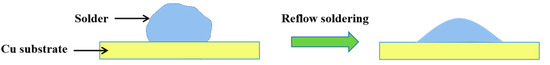
Figure 1.
Schematic diagram of Sn35Bi0.3Ag–xIn alloy solder wettability on a copper substrate.
2.3. Characterization of Material Organization and Properties
After the solder joints were prepared, they were placed in a high-temperature vacuum contact angle meter (Zhongyi Kexin SCI-1400, Beijing, China), and a software package was used to measure the wetting angle of Sn35Bi0.3Ag–xIn solder/Cu. Multiple measurements were taken on the samples to ensure the accuracy of the data. To investigate the effect of In elements on the Sn35Bi0.3Ag–xIn solder/Cu interface, solder joints were cut along the cross-section and set in epoxy resin, and the samples were mechanically ground and polished. Afterward, the solder joint interface was observed using an Hitachi S-3400N SEM scanning electron microscope (Hitachi, Tokyo, Japan), and the interface was analyzed using an energy spectrum analyzer (EDS) to determine the microstructure and constituent elements at the solder joint. Prior to SEM observation, the samples were coated with a sputtered platinum coating to avoid charging effects. In addition, the melting properties of the alloyed solder were analyzed using a comprehensive simultaneous thermal analyzer (NETZSCH STA-409PC, Selb, Germany); the mechanical properties of the solder joint were tested using a universal tensile tester (Shimadzu AG-X100KN, Kyoto, Japan); and the thickness of the intermetallic compound (IMC) was determined using SEM and the measurement tools in Photoshop software (version 23.0, Adobe, San Jose, CA, USA).
3. Results and Discussion
3.1. Differential Heat Analysis
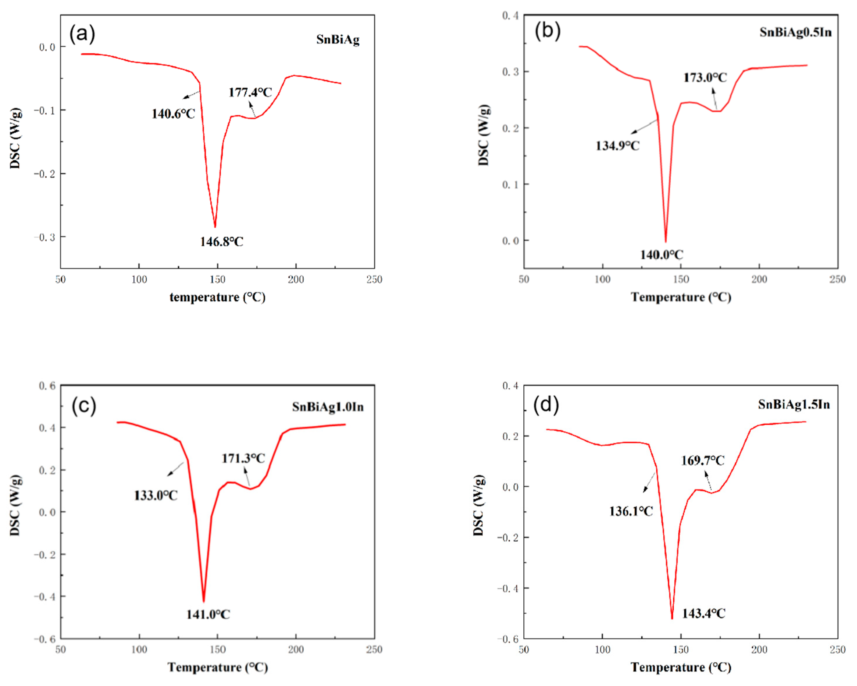
The melting point of the alloy is the basic parameter of the soldering temperature, which determines the temperature setting in the soldering process and has a great influence on the field of surface mount technology (SMT). A superior alloy solder should have a low melting temperature, and the melting interval (melting range) of the solder should be as small as possible, which will help to reduce the process test time, improve the performance of the solder joint, as well as avoid creep problems with the solder after soldering. Figure 2 shows the DSC curves for the SnBiAg–xIn (x = 0, 0.5, 1.0, 1.5) alloy solder. DSC thermal analysis (NETZSCH STA-409PC, Selb, Germany) was carried out at a heating rate of 5 °C/min and heating temperature from room temperature to 250 °C under N2 gas protection. In combination with the binary phase diagram of the Sn–Bi alloy in Figure 3 [26], it can be seen that when the alloy melts, the β-Sn phase with a body-centered cubic structure is precipitated first, after which the Bi-rich phase with a rhombic structure precipitated in the β-Sn phase, which explains the formation of a plateau on the high-temperature side of the heat absorption peak in Figure 2. Table 2 shows the solid-phase line temperature, liquid-phase line temperature, and melting range of the SnBiAg–xIn (x = 0, 0.5, 1.0, 1.5) alloy solder. As can be seen from Table 2, the solid-phase line temperatures of the SnBiAg, SnBiAg0.5In, SnBiAg1.0In, and SnBiAg1.5In alloy solders were 140.6, 134.9, 133.0, and 136.1 °C, respectively. The solid-phase line temperatures of the SnBiAg, SnBiAg0.5In, SnBiAg–1.0In, and SnBiAg–1.5In alloy solders had peak liquid-phase line temperatures of 177.4, 173.0, 171.3, and 169.7 °C, respectively. This indicates that the addition of the In element reduces the solid–liquid phase temperature of the alloy solder. This may be due to the low melting point of the In element (156.6 °C), which reduces the melting point of the SnBiAg alloy; the addition of small amounts of In elements changes the composition of the alloy, which is similar to the quaternary eutectic composition of the SnBiAg–In quaternary system; another reason may be that trace amounts of In elements solidly dissolved in the Sn–Bi matrix, which changes the atomic spacing and thus changes the interatomic bonding force, thus reducing the melting point of the solder. In addition, it can be seen from Table 2 that the solid–liquid phase temperature of the solder alloy decreases with the addition of the In element. Moreover, the melting ranges of the alloyed solders are all less than 8 °C dry from Table 2, which meets the requirements of SMT applications and indicates that the alloy exists in a partially liquid form in a short time during solidification and can form reliable joints during the soldering process.
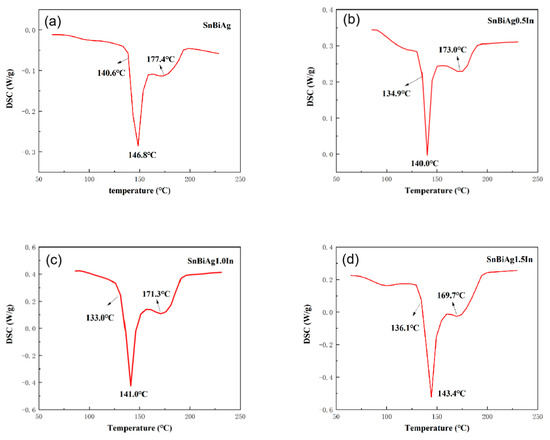
Figure 2.
DSC curves of SnBiAg–xIn (x = 0, 0.5, 1.0, 1.5) alloy solders: (a) SnBiAg, (b) SnBiAg0.5In, (c) SnBiAg1.0In, and (d) SnBiAg1.5In.
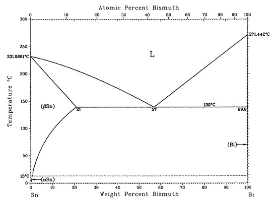
Figure 3.
Phase diagram of Sn–Bi binary alloy [26].
Table 2.
Solid-phase line temperature, liquid-phase line temperature, and melting range of SnBiAg–xIn (x = 0, 0.5, 1.0, 1.5) alloy solders.
3.2. Wettability of Solder Joints SnBiAgIn/Cu
Wettability is a very important material property parameter of solders. Good wetting and spreading ability is a prerequisite for forming good solder joints and directly determines the reliability of the solder joint. The wettability angle of the SnBiAg–xIn (x = 0, 0.5, 1.0, 1.5) alloy solder on the Cu substrate surface is shown in Figure 4. As can be seen from the graph, the wettability of the SnBiAg alloy on the Cu substrate surface is 24.2°, and with the addition of In elements, the wettability of the SnBiAg–xIn alloy solder on the Cu substrate surface first decreases and then increases. When 0.5% In was added, the wettability of the alloy on the Cu substrate is reduced to 21.6°, and when 1.0% In was added, the wettability of the alloy on the Cu substrate is the smallest, which is 19.0°, which is reduced by 21.5%. However, when 1.5% In was added, the wetting angle of the alloy on the Cu substrate surface increases to 27°. This may be due to the addition of a small amount of the In element, reducing the solid–liquidus temperature of the alloy solder and improving the fluidity of the molten solder on the Cu substrate. Another reason may be that the addition of In promotes the diffusion of Cu at the interface, facilitates the interfacial reaction, and reduces the surface tension between the alloy solder and the Cu substrate, thus improving the wettability of the alloy solder on the Cu substrate. However, when excessive amounts (>1.5%) of In was added, the oxidation of In formed a compound on the surface of the molten solder, which hindered the flow of the molten solder, thus reducing the wettability of the solder on the Cu substrate. When the molten solder reaches equilibrium on the Cu substrate, the interfacial tension between the molten solder and the Cu substrate conforms to Young’s equation, which is given as follows:
where γgs is the surface tension between gas and solid; γls is the surface tension between liquid and solid; γlg is the surface tension between liquid and gas; and θ is the wettability angle between liquid, solid, and gas phases [27]. The addition of a small amount (<1.0%) of In reduces the solid–liquid surface tension between the molten solder and the Cu substrate, decreases the wetting angle between the solder and the Cu substrate, and improves the wettability of the alloyed solder on the Cu substrate. In contrast, the addition of excessive (>1.5%) amounts of In elements hinders the flow of the solder, increases the solid–liquid surface tension between the molten solder and the Cu substrate, and reduces the wettability of the alloyed solder on the Cu substrate. In addition, in the relevant literature, based on the empirical relationship of the wetting angle between the solid and liquid surfaces, the best wetting effect is achieved when the wetting angle is greater than 0 and less than 20 degrees [28]. Therefore, in the present study, the SnBiAg–1.0In alloy solder showed the best wetting performance on the surface of the Cu substrate.
cos θ = (γgs − γls)/γlg
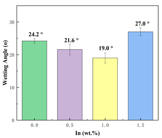
Figure 4.
Wetting angle of SnBiAg–xIn (x = 0, 0.5, 1.0, 1.5) alloy solder on Cu substrate surface.
3.3. SnBiAg–xIn/Cu Interface Organization Analysis
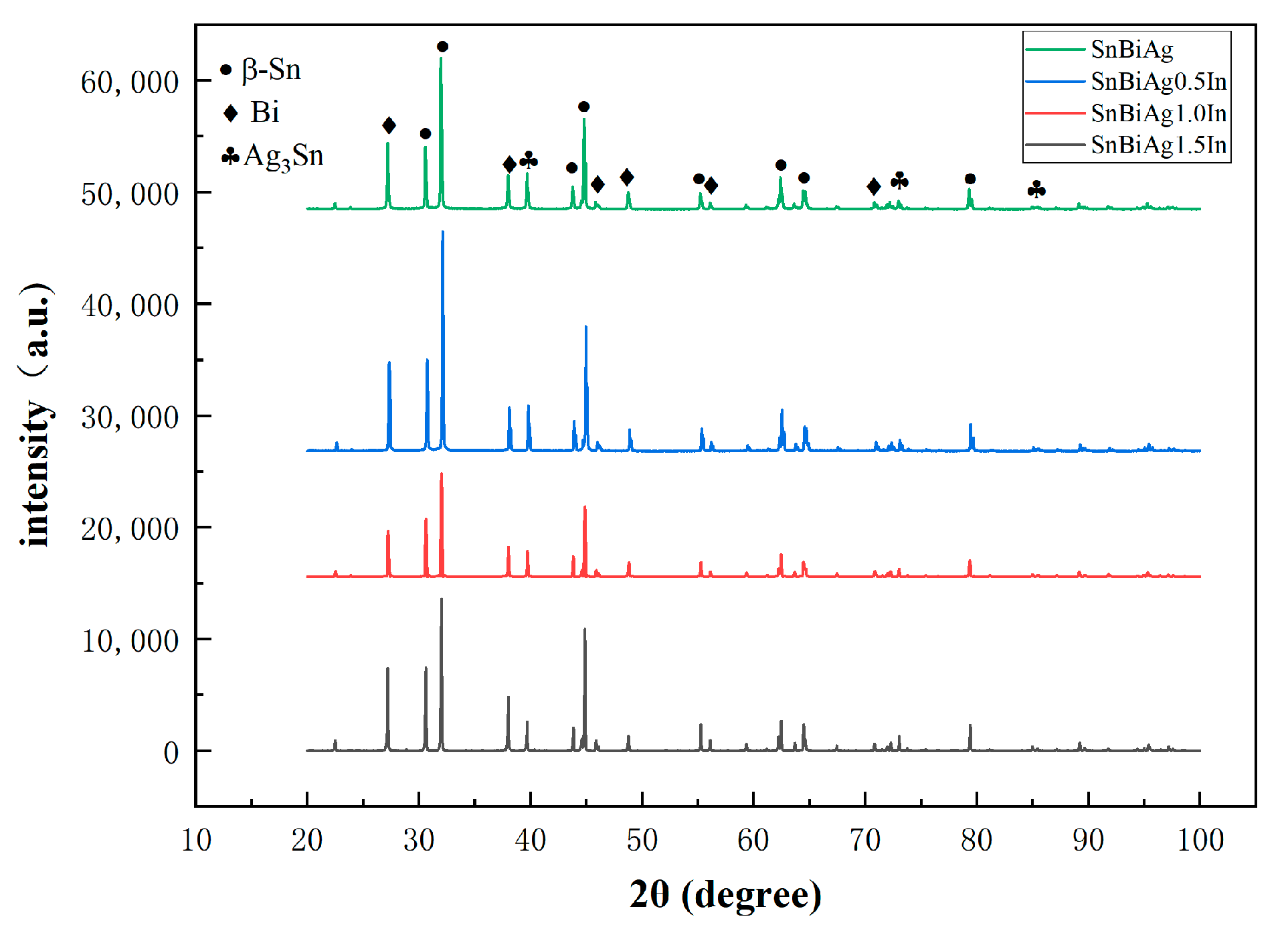
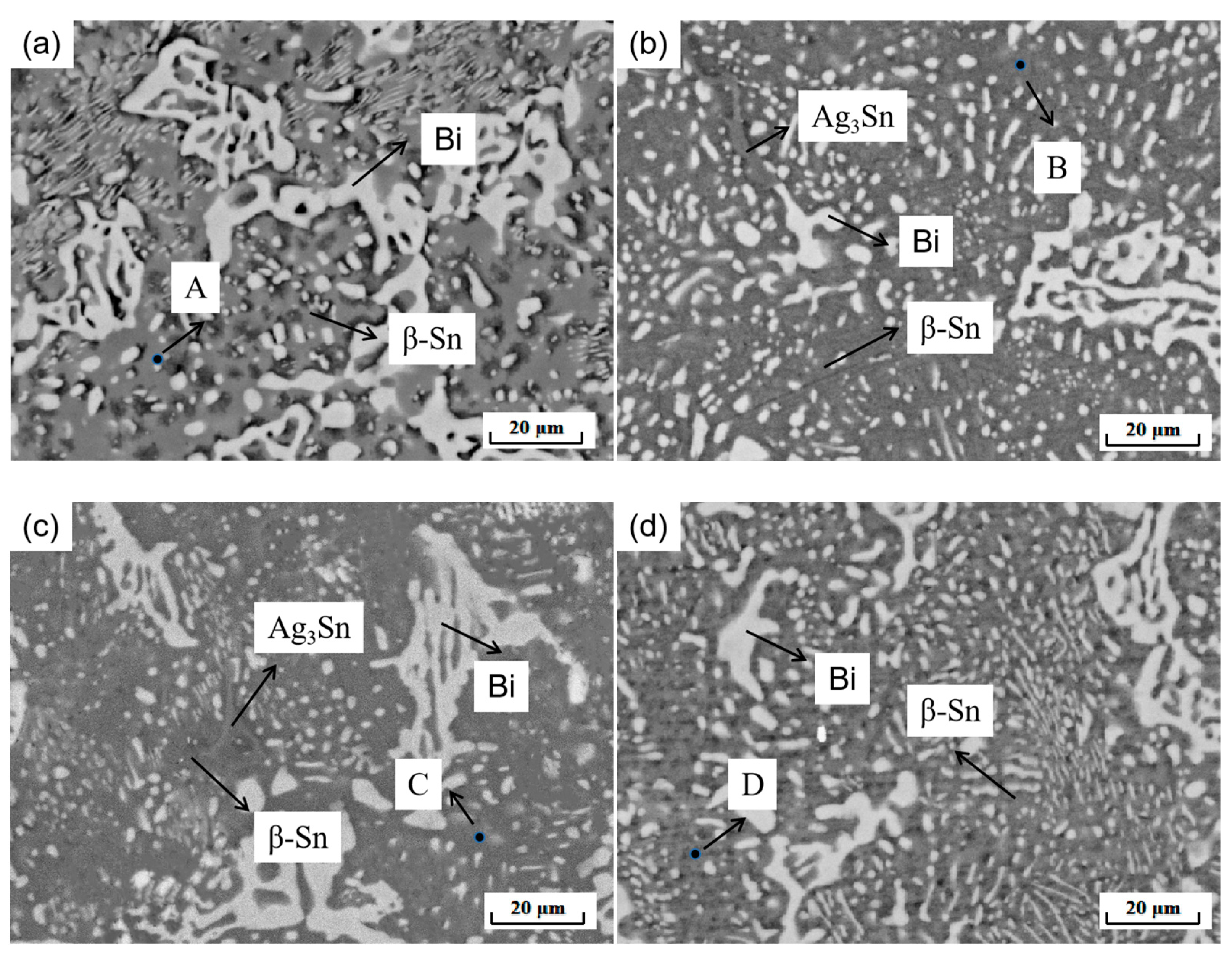
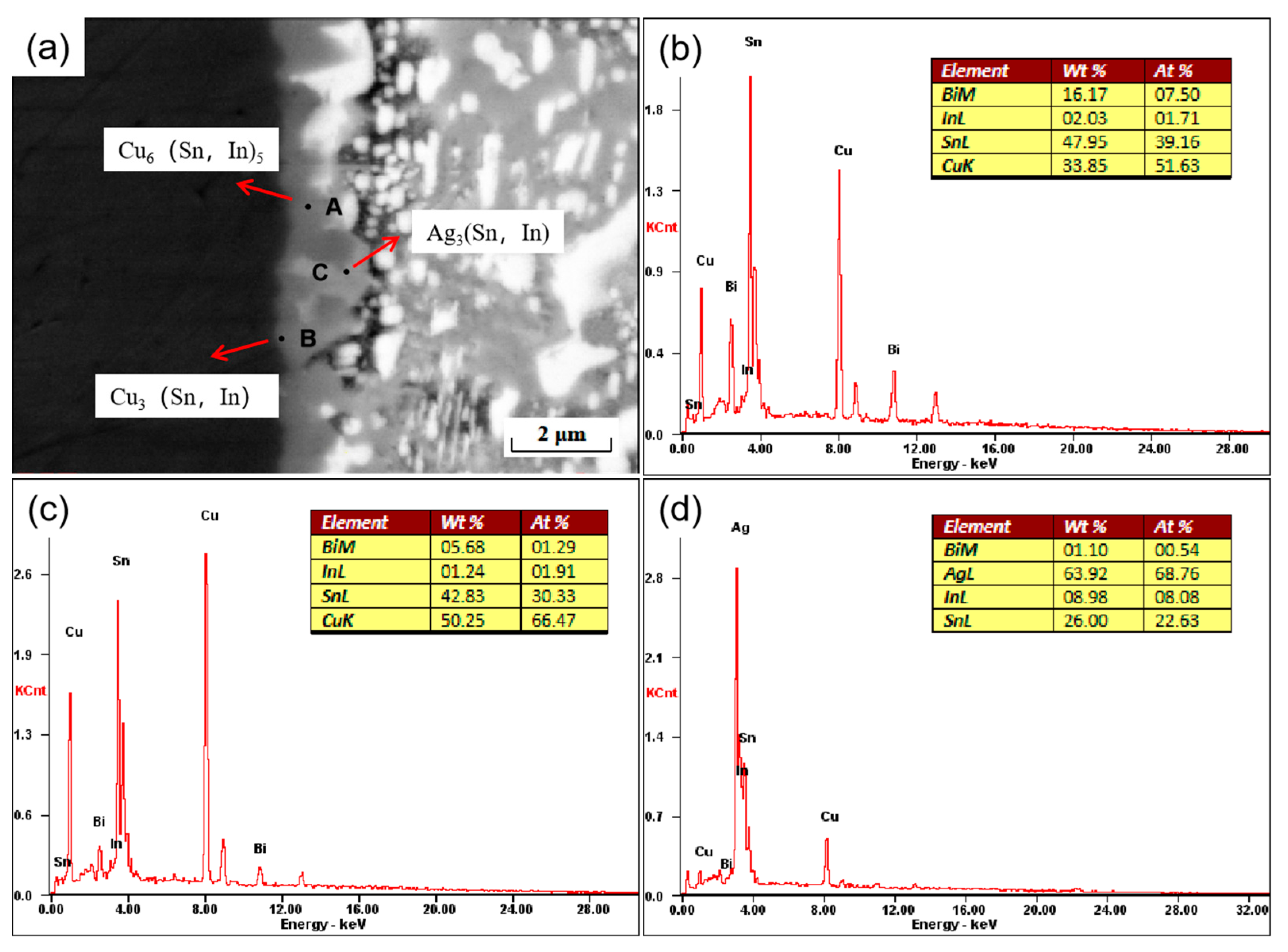
The performance of the material depends on the microstructure of the material. Figure 5 shows the XRD phase analysis results of the SnBiAg–xIn (x = 0, 0.5, 1.0, 1.5) alloy solder. It can be seen from the diagram that there are three phases in the SnBiAg solder: the β-Sn phase with body-centered cubic structure, Bi-rich phase with rhombohedral structure, and Ag3Sn phase with close-packed hexagonal structure. After adding the In element to the solder, no new phase was found. This may be due to the fact that the content of the added In element is too small, and the equipment does not detect it; the second is that Sn has a certain solid solubility for In, and adding a small amount of In creates an almost solid solution in the Sn matrix; the formation of new phases was therefore not found. Figure 6 shows the SEM image of the backscattered electrons of the SnBiAg–xIn (x = 0, 0.5, 1, 1.5) alloy solder. It can be found from the figure that in the alloy solder of type 4, the bright and continuous strip-type Bi phase is uniformly dispersed in the β-Sn matrix, and a small amount of Ag3Sn is uniformly distributed in β-Sn, which can refine the solder structure, improving the mechanical properties of the solder. After adding a small amount of the In element, no new phase was found, indicating that most of In was dissolved in the solder structure, which is consistent with the detection results of XRD. In addition, the Bi phase in the solder structure was obviously refined and more uniformly distributed in the solder matrix, so adding a small amount of the In element can improve the microstructure and properties of the solder. It can be seen from the EDS spectrum (Figure 7) that when 0.5% In was added, the content of the Bi element dissolved in the matrix increases from 6.2% to 11.02%, and the precipitated Bi phase decreases. However, when more than 1.0% In was added, the content of the Bi element dissolved in the matrix decreases to 4.63%, and the precipitated Bi phase increases. This is because In has a crystal structure similar to that of a Sn–Bi solder (all tetragonal crystal system) and also because of the In element's electronegativity, and its atomic radius (1.66) is between Sn (1.58) and Bi (1.7), which makes it easier to form a solid solution (a small lattice distortion when elements with a small atomic radius difference form a solid solution). Therefore, when a small amount (<1.0%) of the In element is added, In will act as a bridge for the solid solution of Sn and Bi elements, improving the solid solubility of the Bi element in the Sn matrix. When the addition of the In element is too much (>1.0%), the distortion energy of the solder system will be reduced, resulting in the precipitation of a part of Bi atoms.
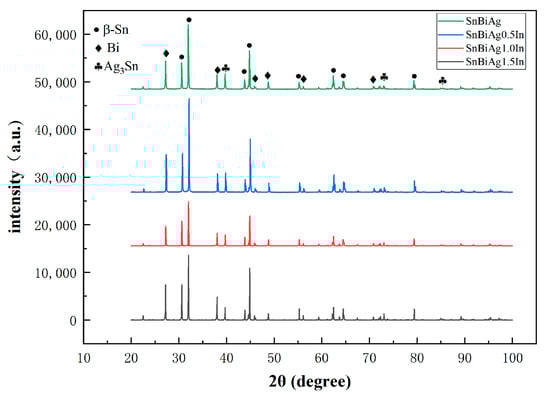
Figure 5.
XRD patterns of SnBiAg–xIn (x = 0, 0.5, 1.0, 1.5) solder alloy.

Figure 6.
Microstructure of SnBiAg–xIn (x = 0, 0.5, 1, 1.5) alloy solder: (a) SnBiAg; (b) SnBiAg0.5In; (c) SnBiAg1.0In; (d) SnBiAg1.5In.
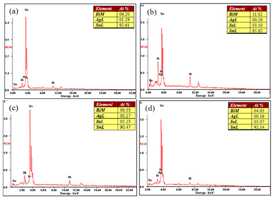
Figure 7.
Energy spectrum analysis of points A (a), B (b), C (c) and D (d).
During the soldering process, the molten solder reacts with the base metal to form a solder joint. The reaction takes place between the solder and metal substrate, and an interfacial layer is formed, the product of which is an intermetallic compound (IMC). The thickness of the interfacial layer as well as the shape, size, and distribution of the intermetallic compound affect the service life of the solder joint, so it is vital to study the interfacial layer and intermetallic compound. As shown in Figure 8, a secondary electron morphology image of a cross-section of a SnBiAg–1.5In/Cu solder joint is shown. From the figure, it can be noticed that there is clearly the formation of an IMC layer between the solder and Cu substrate, indicating that the molten SnBiAg–1.5In solder reacts with the Cu substrate material by interdiffusion at high temperatures. At the SnBiAg–1.5In solder/Cu interface, the generated IMC was observed to be scallop-shaped. As shown in Figure 8b–d, the composition of the phase of the IMC at the interface can be inferred from the EDS energy spectrum analysis. From the results, it can be seen that at point A, the atomic percentages of Cu and Sn elements are 51.63% and 39.16%, respectively, with the ratio of Cu to Sn being approximately 6:5. In addition, 1.71% of the In element was also present, so it is presumed that point A is the Cu6 (Sn, In)5 phase, which is different from the Cu6 Sn5 phase generated by the Cu–Sn system because the In and Sn crystal structures are the same and the atomic radii are close. The Cu6 (Sn, In)5 phase is produced in the interfacial layer as a result of the substitution of some of the Sn atoms by In atoms in the compound. At point B, near the Cu substrate, the atomic percentages of Cu, Sn, and In elements are 66.47%, 30.33%, and 1.91%, respectively, so it is presumed that not only the Cu6 (Sn, In)5 phase but also the Cu3 (Sn, In) phase is formed at point B. The interfacial reaction process of SnBiAg–1.5In/Cu is similar to the Sn–Cu interfacial diffusion process. During soldering, the Cu–Sn bonding interface diffuses into each other. Since the diffusion rate of Cu into Sn is greater than the diffusion rate of Sn into Cu [29], at the beginning of soldering, Cu will diffuse into Sn and thus react with Sn, and the In atoms will be replaced with some of the Sn atoms after diffusion into the interface layer. Later, as the soldering time increases, the IMC moves toward the center of the joint, the thickness of the Cu6 (Sn, In)5 layer increases, and the rate of diffusion of Cu into Sn decreases, gradually generating a scalloped Cu3 (Sn, In) phase. The reaction process is given as follows:
6Cu + 5Sn − Cu6Sn5
Cu6Sn5 + 5(1 − x)In − Cu6(Sn, In)5 + 5(1 − x)Sn
Cu6(Sn, In)5 + 9Cu − Cu3(Sn, In)
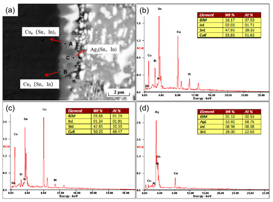
Figure 8.
Interface of SnBiAg–1.5In/Cu solder joints: (a) microstructure and (b) EDS analysis of zone A, (c) zone B, and (d) zone C.
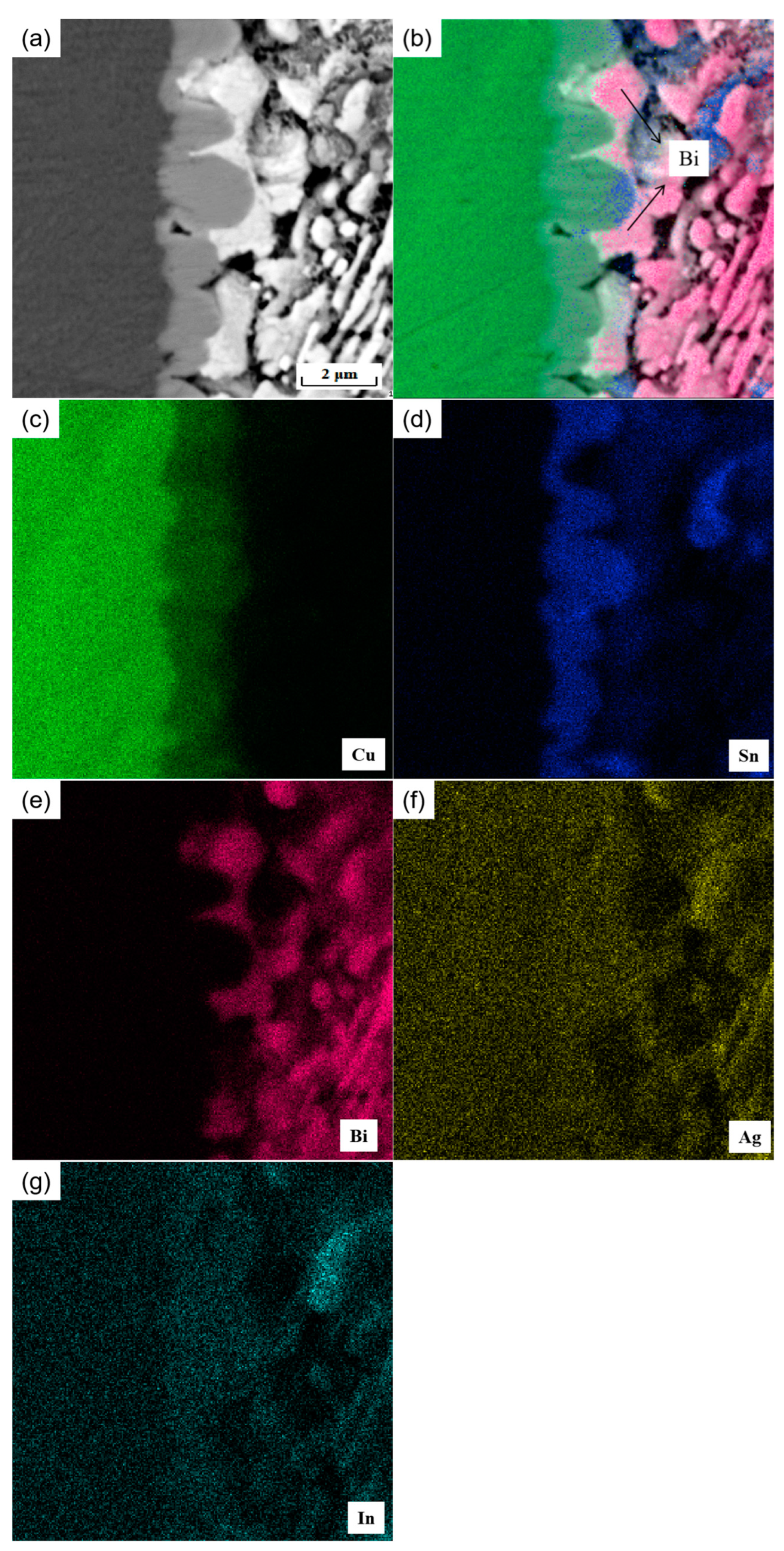
Moreover, it is found that at the interface, in addition to the Cu6 (Sn, In)5 and Cu3 (Sn, In) phases, there are also the C phase labeled in the figure. The atomic percentages of the elements Ag, Sn, and In were 68.76%, 22.63%, and 8.08%, respectively, as analyzed by the EDS energy spectrum (Figure 8d), which is presumed to be the Ag3 (Sn, In) phase. In Figure 8a, the thickness of the IMC layer near the Ag3 (Sn, In) phase in the interfacial region is thinner than the other parts without the Ag3 (Sn, In) phase. This indicates that the presence of the Ag3 (Sn, In) phase inhibits the growth of Cu6 Sn5 in the solder interface. This is mainly due to two reasons: the formation of the Ag3 (Sn, In) phase consumes the Sn atoms in the adjacent area, reducing the possibility of Cu–Sn reaction at the solder interface; and the formation of the Ag3 (Sn, In) phase hinders the diffusion of Sn from the solder matrix to the solder–IMC interface. Figure 9 shows the elemental surface sweep of the solder cross-interface for SnBiAg–1.5In/Cu. From the figure, it can be found that the In element is uniformly distributed in the IMC layer, indicating that the In element is involved in the generation of the interfacial reaction layer. Moreover, from Figure 9b, it can be found that there is the presence of the Bi phase on one side of the interface, which hinders the growth of the IMC layer and reduces the thickness of the interface layer, which is conducive to improving the performance of the solder joint.
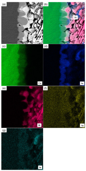
Figure 9.
Microstructure and elemental surface sweep of SnBiAg–1.5In/Cu interface: (a) SEM image, (b) elemental surface distribution, (c) Cu, (d) Sn, (e) Bi, (f) Ag, and (g) In.
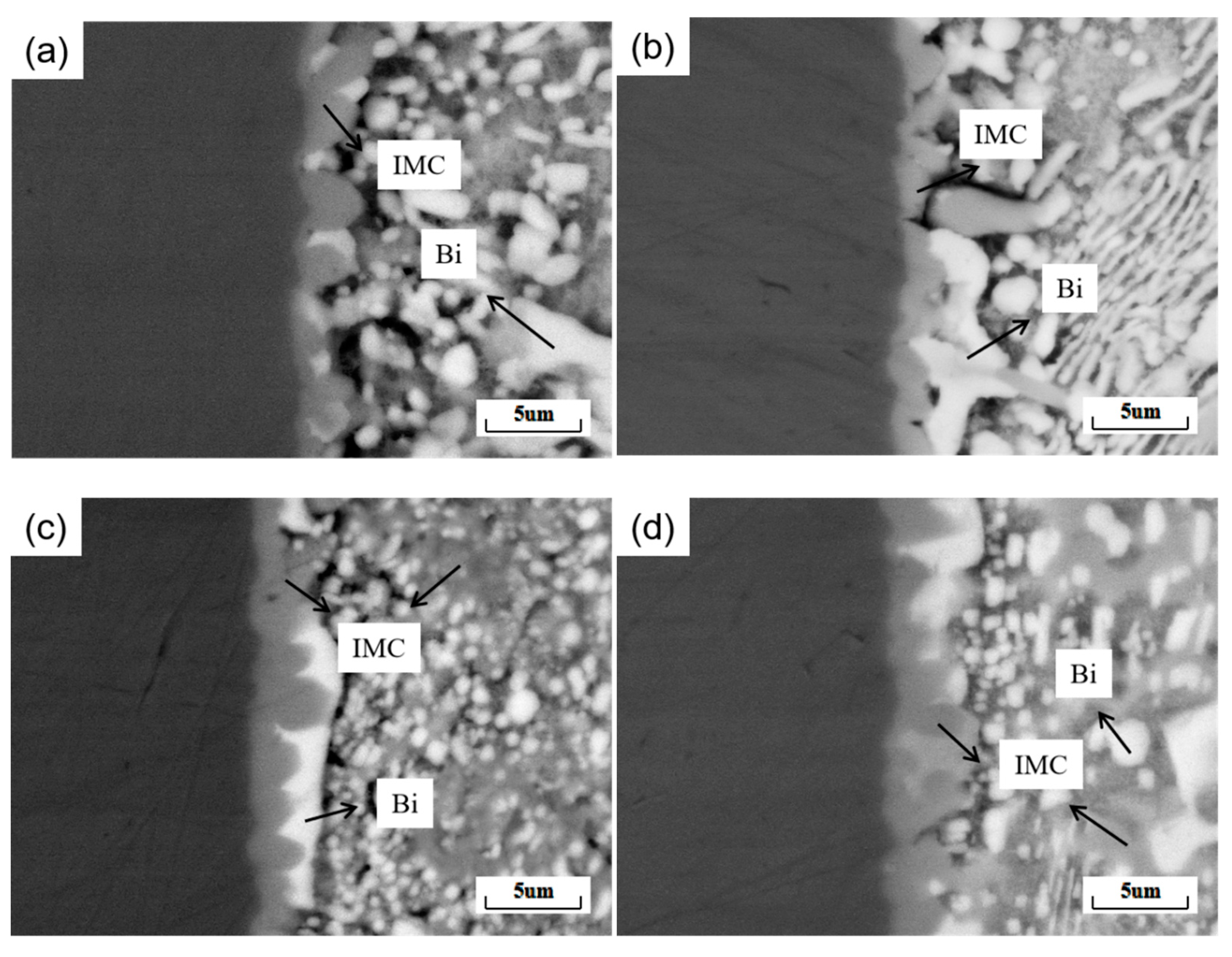
The formation of an interfacial IMC layer indicates the chemical bond between the solder and substrate. However, excessive growth of the IMC layer can seriously affect the mechanical reliability of the solder joint and can reduce the service life of electronic components. It is essential to study the interfacial IMC layer in solder systems. Figure 10 shows the secondary electron morphology of a cross-section of a SnBiAg–xIn/Cu (x = 0, 0.5, 1.0, 1.5) soldered joint. As can be seen from the figure, the IMCs all grow in a scalloped form, but with the addition of In elements, there are some differences in the shape, size, and densities of the IMCs. In order to further investigate the effect of different levels of In elements on the IMC layer at the SnBiAg–xIn/Cu interface, the thickness of the IMC layer was calculated. The average thickness of the IMC layer can be measured using the following equation [30]:
where χ is the average thickness of the IMC layer, A is the integral area of the IMC layer, and L is the length of the IMC layer. Figure 11 shows the average thickness of the IMC at the interface of SnBiAg–xIn/Cu (x = 0, 0.5, 1.0, 1.5) joints. When a small amount (<1.0%) of In is added, the Bi phase appears on the solder side of the interface layer, which hinders the growth of the IMC, so the IMC tends to grow in layers and the IMC layer thickness slightly decreases; the thickness of the IMC layer is reduced to 1.25 μm, which is reduced by 14.4%. However, when 1.5% of In was added, the Bi phase on the solder side of the interface layer decreased, and the IMC layer thickness increased to 1.78 μm. Similarly, Yun et al. demonstrated that the Bi phase on the solder side had an inhibitory effect on IMC growth [31] and that the different interfacial energies of the IMC in the Sn and Bi phases resulted in different growth rates. As a result, the grain curvature becomes larger, and the IMC layer is flatter when the IMC is in contact with the Bi phase. Compared with the Sn58Bi0.4Ag/Cu interface IMC thickness (1.54 μm) [32], adding a small amount of the In element (<1.5%) can significantly reduce the interface layer thickness. In addition, Figure 10b–d show strips of the IMC extending into the solder, as well as large pieces of the IMC in a free state. This is due to the fact that during the growth of the IMC, the part that extends into the brazing material grows in an orientation and undergoes a necking-fracture-deflection process as it continues to elongate [33].
χ = A/L

Figure 10.
Secondary electron morphology of SnBiAg–xIn/Cu (x = 0, 0.5, 1.0, 1.5) solder joint cross-sections: (a) SnBiAg/Cu; (b) SnBiAg0.5In/Cu; (c) SnBiAg1.0In/Cu; (d) SnBiAg1.5In/Cu.
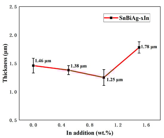
Figure 11.
Average thickness of IMC at interface of SnBiAg–xIn/Cu (x = 0, 0.5, 1.0, 1.5) solder joints: 1.46 μm—SnBiAg/Cu; 1.38 μm—SnBiAg0.5In/Cu; 1.25 μm—SnBiAg1.0In/Cu; 1.78 μm—SnBiAg1.5In/Cu.
3.4. Analysis of Atomic Diffusion Processes
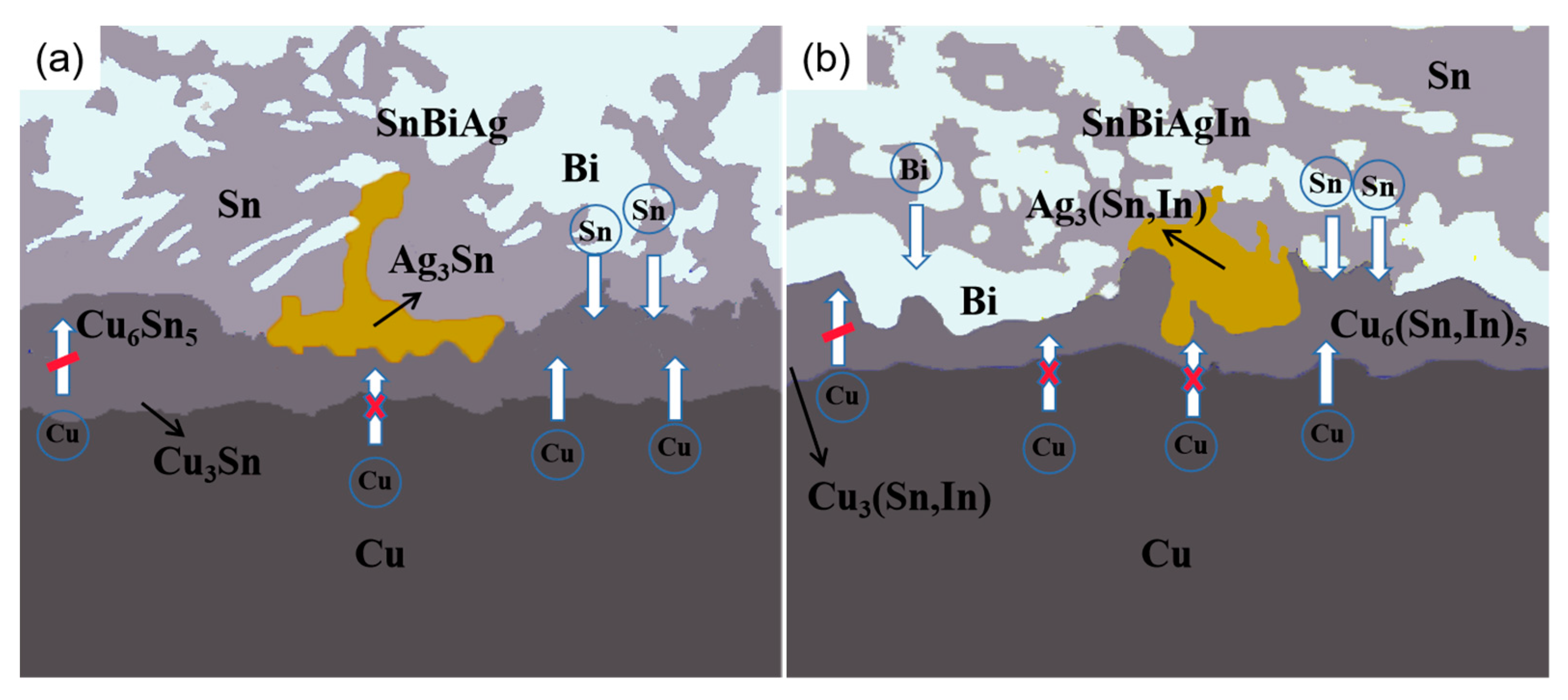
The growth of the IMC is one of the main features of the evolution of the interface organization of a solder joint and is an important factor in the analysis of the reliability of solder joints. Both the diffusion of atoms during the soldering process and the solid–liquid phase reaction between the interfaces play a crucial role in the growth of the IMC. The diffusion of atoms during the reaction at the SnBiAg/Cu interface is shown in Figure 12a. As the solder temperature increases, the solder starts to melt and the Cu atoms start to move toward the solder side, with fine Cu6 Sn5 grains nucleating and growing at the interface first. With the increase in the soldering time, the Cu6 Sn5 phase grows and its thickness gradually increases. The layered Cu6 Sn5 hinders the diffusion of Cu atoms to the interface. As a result, the Cu atoms gradually react with Cu6 Sn5, and the Cu3 Sn phase is formed at the interface. Subsequently, the Cu and Sn atoms continue to diffuse into each other. Cu6 Sn5 and Su3 Sn grow one after another, and the IMC layer thickness gradually increases. Since the Cu3 Sn phase generated requires more activation energy [34], the Cu6 Sn5 grows much faster than the Cu3 Sn. The Ag atoms themselves will generate the Ag3 Sn phase with the solder. During the interfacial reaction, the Ag3 Sn phase will gradually diffuse onto the surface of the IMC, hindering the diffusion of Cu atoms and thus reducing the thickness of the IMC layer. As can be seen in Figure 12b, the addition of In atoms is broadly similar to the SnBiAg/Cu interfacial reaction, but it changes the phase structure of the IMC, generating Cu6 (Sn, In)5, Cu3 (Sn, In), and Ag3 (Sn, In) phases during the diffusion process, which is due to the fact that In and Sn have the same crystal structure and close atomic radii, and part of the Sn atoms in the compound is replaced by In atoms. Moreover, the addition of the In element changes the activation energy at the interface and reduces the diffusion rate of Cu and Sn atoms, thus reducing the thickness of the IMC layer [35]. The addition of the In element also lowers the melting point of the solder and changes the diffusion rate of the Bi element in the solder; thus, during diffusion, the Bi atoms are influenced by the In element and will diffuse toward the interface, and when diffusion reaches the IMC layer, it will be hindered by the Cu6 (Sn, In)5 and stops, after which it accumulates at the IMC layer, which, in turn, has an inhibiting effect on the IMC and reduces the growth of the IMC layer. Based on the above results and discussion, it can be seen that the IMC at the SnBiAg/Cu interface is mainly Cu6 Sn5, whose growth rate is mainly controlled by the diffusion of Cu elements in the substrate and Sn elements in the solder. The IMC at the SnBiAg1.0In/Cu interface is mainly Cu6 (Sn, In)5, and its growth rate is not only controlled by the diffusion of the Cu element in the matrix and the Sn element in the solder but also affected by the In element. The Bi and Ag3 (Sn, In) phases formed at the interface also affect the growth of the IMC.
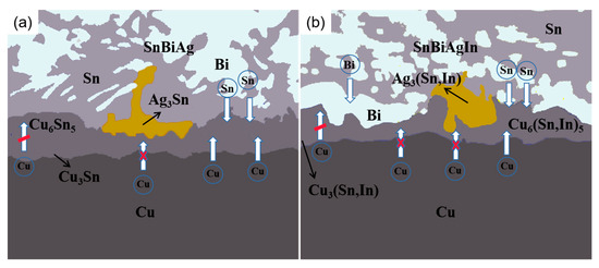
Figure 12.
Schematic diagram of diffusion of elements in IMC during soldering: (a) SnBiAg; (b) SnBiAgIn.
3.5. Shear Strength and Failure Analysis of SnBiAg–xIn/Cu Soldered Joints
The generation of a thin and continuous IMC layer during soldering is necessary for good wetting and joining and will also improve the mechanical properties of the soldered joint. Figure 13 shows the shear strength of the SnBiAg–xIn (x = 0, 0.5, 1.0, 1.5)/Cu soldered joint. It is clear from the graph that the shear strength of the SnBiAg/Cu soldered joint is 52.1 MPa and that the addition of In elements can increase the shear strength of the alloy solder to the Cu matrix. When a small amount of In (<1.0%) is added, the shear strength of the soldered joint significantly increases from 52.1 MPa to 55.1 MPa; when 1.5% In is added, the shear strength of the soldered joint decreases instead, falling to 42.5 MPa. Since the IMC is mostly brittle, an excessively thick IMC layer can significantly reduce the reliability of the soldered joint. Combined with the analysis in Figure 7, the addition of a small amount of In elements leads to the increase in the Bi phase on the solder side, which hinders the growth of the IMC and reduces the thickness of the IMC layer, thus improving the shear strength of the soldered joint; with the addition of more In elements, the Bi phase on the solder side disappears and does not slow down the growth of the IMC, and because In elements will partially replace the Sn in the Cu6 Sn5 compound, generating the Cu6 (Sn, In)5 phase, it will make the lattice fit between the different components of the joints weaker, resulting in a reduction in the bonding of the IMC to the Cu matrix and thus reducing the shear strength of the soldered joint.
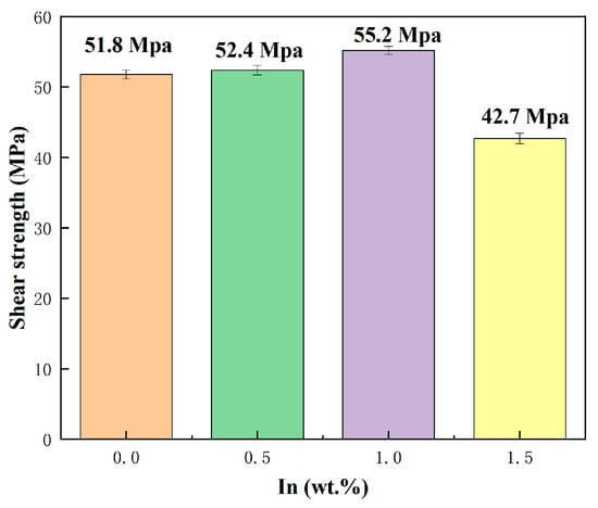
Figure 13.
Shear strength of SnBiAg–xIn (x = 0, 0.5, 1.0, 1.5)/Cu soldered joints.
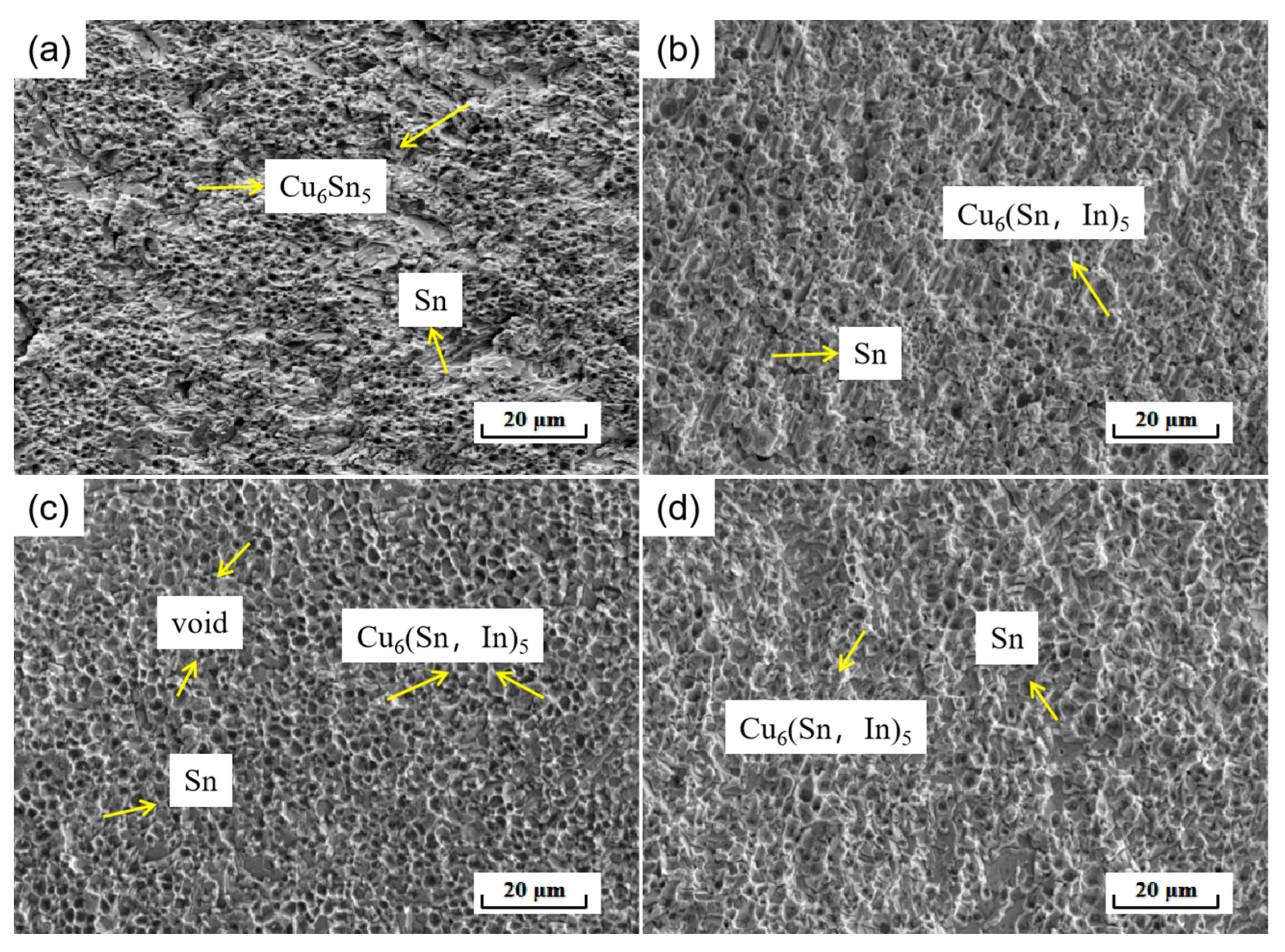
In order to further investigate the effect of In elements on the mechanical properties of soldered joints, the fracture morphology of soldered joints was analyzed. As shown in Figure 14, which shows the fracture microscopic morphology of SnBiAg–xIn (x = 0, 0.5, 1.0, 1.5)/Cu soldered joints, the differences in cracking sites and fracture morphology are not very different despite the differences in solder composition. As can be seen in Figure 14a, the fracture profile is relatively flat in macroscopic terms, indicating that the fracture occurred on the Cu/IMC/solder side of the soldered joint. This is because there is a large gap in mechanical properties between the solder and interface, and the different coefficients of thermal expansion and stress concentration at the interface lead to fracture at the interface. EDS spectroscopy of the fracture matrix and the particles attached to it shows that the fracture matrix is Sn-based (91.59% Sn atoms), and the particles attached to it are Cu6 Sn5 (51.23% Cu, 47.35% Sn atoms, approximate atomic ratio 6:5), indicating that the fracture of the soldered joint occurred from the IMC/solder side. The fracture morphology shows some typical cleavage fracture characteristics. With the addition of small amounts (<1.0%) of In elements, the fracture profile shows that the cleavage fracture characteristics are reduced. The fracture morphology in Figure 14b shows a certain selective orientation of the fracture morphology after pulling. The large number of neat and fine cavities (caused by Cu6 (Sn, In)5 grains being pulled out) left on the fracture surface (Figure 14c) explains the higher shear strength of the SnBiAg1.0In/Cu soldered joint. As can be seen in Figure 14d, the fracture morphology shows more cleavage fracture characteristics when 1.5% of the In element is added, with no apparent grain orientation of the fracture surface. According to the above results and discussion, it can be seen that the fracture of the solder joint occurs on the IMC–solder side and that the addition of 1.0% of the In element reduces the brittle fracture characteristics of the joint and improves the shear strength of the joint.
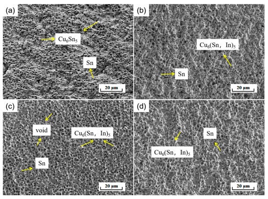
Figure 14.
Fracture microstructure of SnBiAg–xIn (x = 0, 0.5, 1.0, 1.5)/Cu soldered joints: (a) SnBiAg/Cu; (b) SnBiAg0.5In/Cu; (c) SnBiAg1.0In/Cu; (d) SnBiAg1.5In/Cu.
4. Conclusions
In this experiment, a SnBiAg–xIn (x = 0, 0.5, 1.0, 1.5) alloy solder was successfully prepared, the thermomechanical properties of the alloy solder and the wettability properties on the Cu substrate were investigated, the effect of In elements on the interfacial organization and mechanical properties of SnBiAg–xIn/Cu joints was analyzed, and the following conclusions were drawn.
- The result of the differential thermal analysis shows that the addition of In elements reduces the solid–liquid phase temperature of the alloy solder. The SnBiAg–xIn (x = 0, 0.5, 1.0, 1.5) alloy solder has a small melting range of 8 °C and forms reliable joints during the soldering process.
- The wettability of the SnBiAg–xIn alloy solder on the surface of the Cu substrate first increases and then decreases with the addition of In elements. When 1.0% of the In element is added, the wettability angle of the alloy on the Cu substrate surface is the smallest at 19.0°.
- At the SnBiAg1.0In/Cu interface, where the In atoms replace some of the Sn atoms, the IMC is mainly Cu6 (Sn, In)5, whose growth rate is controlled by the diffusion of the Cu elements in the matrix and the Sn elements in the solder, but is also influenced by the In elements. The Bi and Ag3 (Sn, In) phases formed at the interface also affect the growth of the IMC.
- The SnBiAg–xIn (x = 0, 0.5, 1.0, 1.5)/Cu joint fractures from the IMC–solder side. Its shear strength first increases and then decreases with the addition of In elements. The highest shear strength of 55.1 MPa was achieved when 1.0% of In was added to the soldered joint.
Author Contributions
B.S. and M.X. (Ming Xie) conceived and designed the experiments; S.Y. and B.S. performed the experiments; G.L. and J.Z. analyzed the data; M.X. (Mingyue Xu) and Q.Z. contributed reagents/materials/analysis tools; B.S. wrote the paper. All authors have read and agreed to the published version of the manuscript.
Funding
This research was funded by the Ministry of Science and Technology of the People’s Republic of China under the National Key Project of “Science and Technology for Economic Development 2020 (SQ2020YFF0426390)”; Major Science and Technology Project of Yunnan Province (202002AB080001-1-6); Genetic Engineering of Rare Precious Metal Materials in Yunnan Province (202002AB080001-6); Major Science and Technology Project of Yunnan Province (202002AB080001-1); Science and Technology Talent and Platform Program of Yunnan Province (202105AC160002, 202105AE160027); and National Natural Science Foundation of China (51961016).
Institutional Review Board Statement
Not applicable.
Informed Consent Statement
Not applicable.
Data Availability Statement
Not applicable.
Acknowledgments
The authors would like to thank Kunming Institute of Precious Metals, State Key Laboratory of Advanced Technologies for Comprehensive Utilization of Platinum Metals, Sino-Platinum Metals Co., Ltd., for providing us with the solder materials.
Conflicts of Interest
The authors declare no conflict of interest.
References
- Zhang, L.; Han, J.G.; Guo, Y.H.; Sun, L. Properties and microstructures of SnAgCu-xEu alloys for concentrator silicon solar cells solder layer. Sol. Energy Mater Sol. Cells 2014, 130, 397–400. [Google Scholar] [CrossRef]
- Peng, F.; Liu, W.; Ma, Y.; Liang, C.; Huang, Y.; Tang, S. Microstructure of Sn-20In-2.8Ag solder and mechanical properties of joint with Cu. Solder Surf. Mt. Technol. 2019, 31, 1–5. [Google Scholar] [CrossRef]
- Gao, L.; Xue, S.; Liang, Z.; Zhong, S.; Feng, J.; Wei, D.; Yu, S.L.; Zeng, G. Effect of alloying elements on properties and microstructures of SnAgCu solders. Microelectron. Eng. 2010, 87, 2025–2034. [Google Scholar] [CrossRef]
- Tong, H.M.; Lai, Y.S.; Wong, C.P. Advanced Flip Chip Packaging. Springer: Boston, MA, USA, 2013; pp. 52–69. ISBN 978-1-4419-5767-2. [Google Scholar]
- Ren, G.; Wilding, I.J.; Collins, M. Alloying influences on low melt temperature SnZn and SnBi solder alloys for electronic interconnections. J. Alloys Compd. 2016, 665, 251–260. [Google Scholar] [CrossRef]
- Xu, K.K.; Zhang, L.; Gao, L.L.; Jiang, N.; Zhong, S.J. Review of microstructure and properties of low temperature lead-free solder in electronic packaging. Sci. Technol. Adv. Mater. 2020, 21, 689–711. [Google Scholar] [CrossRef]
- Liu, Y.; Tu, K.N. Low melting point solders based on Sn, Bi, and In elements. Mater. Today Adv. 2020, 8, 100115. [Google Scholar] [CrossRef]
- Zhu, W.; Zhang, W.; Zhou, W.; Wu, P. Improved microstructure and mechanical properties for SnBi solder alloy by addition of Cr powders. J. Alloys Compd. 2019, 789, 805–813. [Google Scholar] [CrossRef]
- Shiue, Y.Y.; Chuang, T.H. Effects of la addition on microstructure and mechanical properties of SN-58BI solders joints with osp pads. Can. Metall. Q. 2013, 52, 285–294. [Google Scholar] [CrossRef]
- Bang, J.O.; Lee, H.S.; Jung, S.B. Fabrication of Sn-58Bi-xCe Solder Paste Using Electrical Wire Explosion Method and its Mechanical Property. J. Nanosci. Nanotechnol. 2017, 17, 3033–3037. [Google Scholar] [CrossRef]
- Kanlayasiri, K.; Ariga, T. Physical properties of Sn58Bi-xNi lead-free solder and its interfacial reaction with copper substrate. Mater. Des. 2015, 86, 371–378. [Google Scholar] [CrossRef]
- Zhou, S.; Shen, Y.A.; Uresti, T.; Shunmugasamy, V.; Nishikawa, H. Effects of In and Zn Double Addition on Eutectic Sn-58Bi Alloy. In Proceedings of the 2019 IEEE 69th Electronic Components and Technology Conference (ECTC), Las Vegas, NV, USA, 28–31 May 2019. [Google Scholar]
- Wu, S.C.; Lin, S.K.; Nguyen, T.L. Effective suppression of interfacial intermetallic compound growth between Sn-58 wt.% Bi solders and Cu substrates by minor Ga addition. J. Alloys Compd. 2014, 586, 319–327. [Google Scholar]
- Li, J.F.; Mannan, S.H.; Clodm, P. Interfacial reactions between molten Sn-Bi-X solders and Cu substrates for liquid solder interconnects. Acta Mater. 2006, 54, 2907–2922. [Google Scholar] [CrossRef]
- Li, Q.; Lin, J.; Lei, Y.P. Design and properties of Sn-Bi-In low-temperature solders. In Proceedings of the International Conference on Electronic Packaging Technology (Volume 16th International Conferenceon Electronic Packaging), Changsha, China, 11–14 August 2015. [Google Scholar]
- Xue, F.; Chen, X.; Yao, Z. Effect of In on microstructure, thermodynamic characteristic and mechanical properties of Sn-Bi based lead-free solder. J. Alloys Compd. 2015, 633, 377–383. [Google Scholar]
- Shalaby, R.M. Effect of silver and indium addition on mechanical properties and indentation creep behavior of rapidly solidified Bi–Sn based lead-free solder alloys. Mater. Sci. Eng. A 2013, 560, 86–95. [Google Scholar] [CrossRef]
- Yoon, J.W.; Noh, B.I.; Kim, B.K.; Shur, C.C.; Jung, S.B. Wettability and interfacial reactions of Sn–Ag–Cu/Cu and Sn–Ag–Ni/Cu solder joints. J. Alloys Compd. 2009, 486, 142–147. [Google Scholar] [CrossRef]
- Rosa, D.M.; Spinelli, J.E.; Osório, W.R.; Garcia, A. Effects of cell size and macrosegregation on the corrosion behavior of a dilute Pb-Sb alloy. J. Power Sources 2006, 162, 696–705. [Google Scholar] [CrossRef]
- Donelan, P. Modelling microstructural and mechanical properties of ferritic ductile cast iron. Mater. Sci. Technol. 2000, 16, 261–269. [Google Scholar]
- Petch, N.J. The cleavage strength of polycrystals. J. Iron Steel Inst. 1953, 174, 25–31. [Google Scholar]
- Bonatti, R.S.; Siqueira, R.R.; Padilha, G.S.; Bortolozo, A.D.; Osorio, W.R. Distinct Alp/Sip composites affecting its densification and mechanical behavior. J. Alloys Compd. 2018, 757, 434–447. [Google Scholar] [CrossRef]
- Ma, K.; Lavernia, E.J.; Schoenung, J.M. Particulate reinforced aluminum alloy matrix composites e a review on the effect of microconstituents. Rev. Adv. Mater. Sci. 2017, 48, 91–104. [Google Scholar]
- Bouvard, D. Densification behaviour of mixtures of hard and soft powders under pressure. Powder Technol. 2000, 111, 231–239. [Google Scholar] [CrossRef]
- Meyer, Y.A.; Bonatti, R.S.; Bortolozo, A.D.; Osório, W.R. Electrochemical behavior and compressive strength of Al-Cu/xCu composites in NaCl solution. J. Solid State Electrochem. 2021, 25, 1303–1317. [Google Scholar] [CrossRef]
- Venkatraman, M.; Neumann, J.P. Binary Alloy Phase Diagrams. Mater. Eng. 1990, 86–87. [Google Scholar]
- Sun, H. Bi-Based High Temperature Lead-Free Solder Wetting and High Temperature Aging. Yan Shan University: Qinhuangdao, China, 2018. [Google Scholar]
- Kripesh, V.; Teo, M.; Tai, C.T.; Vishwanadam, G.; Mui, Y.C. Development of a lead free chip scale package for wireless applications. In Proceedings of the 51st Electronic Components and Technology Conference, Orlando, FL, USA, 29 May–1 June 2001; pp. 665–670. [Google Scholar]
- Tan, A.T.; Ai, W.T.; Yusof, F. Influence of nanoparticle addition on the formation and growth of intermetallic compounds (IMCs) in Cu/Sn–Ag–Cu/Cu solder joint during different thermal conditions. Sci. Technol. Adv. Mater. 2015, 16, 3. [Google Scholar]
- Fan, Y.; Liang, Z.; Zhi-Quan, L.; Su, Z.; Jia, M.; Li, B. Effects of CuZnAl particles on properties and microstructure of Sn-58Bi solder. Materials 2017, 10, 558–568. [Google Scholar]
- Ma, Y.Z.; Luo, H.T.; Liu, W.S.; Huang, Y.F.; Yu, Q.; Jun, Y. Effects of Bi addition on interfacial reactions and mechnical properties of In-3Ag-xBi/Cu solder joints.Journal of Materials Science. Mater. Electron. 2016, 271, 103–110. [Google Scholar] [CrossRef]
- Chang, S.Y.; Tsao, L.C.; Wu, M.W.; Chen, C.W. The morphology and kinetic evolution of intermetallic compounds at Sn-Ag-Cu solder/Cu and Sn-Ag-Cu-0.5Al2O3 composite solder/Cu interface during soldering reaction. J. Mater. Sci. Mater. Electron. 2012, 23, 100–107. [Google Scholar] [CrossRef]
- Gain, A.K.; Zhang, L. Growth mechanism of intermetallic compound and mechanical properties of nickel (ni) nanoparticle doped low melting temperature tin–bismuth (sn–bi) solder. J. Mater. Sci. Mater. Electron. 2016, 27, 781–794. [Google Scholar] [CrossRef]
- Guo, M.; Sun, F.; Yin, Z. Microstructure evolution and growth behavior of Cu/SAC105/Cu joints soldered by thermo-compression bonding. Solder. Surf. Mt. Technol. 2019, 31, 0911–0954. [Google Scholar] [CrossRef]
- Mokhtari, O.; Nishikawa, H. Effects of In and Ni Addition on Microstructure of Sn-58Bi Solder Joint. J. Electron. Mater. 2014, 43, 4158–4170. [Google Scholar] [CrossRef]


Publisher’s Note: MDPI stays neutral with regard to jurisdictional claims in published maps and institutional affiliations. |
© 2022 by the authors. Licensee MDPI, Basel, Switzerland. This article is an open access article distributed under the terms and conditions of the Creative Commons Attribution (CC BY) license (https://creativecommons.org/licenses/by/4.0/).