Abstract
The early-stage M23C6 morphology at the phase boundary between austenite and δ ferrite grain in Type 304L austenitic stainless steel was investigated with transmission electron microscopy (TEM). The M23C6 has coherency with austenite grains at phase boundary. The phase boundary between the M23C6 and austenite grains has curved appearance. The curved phase boundary might be a faceted interface composed of (111) plane and the other low-index planes on the atomic scale. The M23C6 morphology at the phase boundary was identified to be a complex pyramid-like shape that has {111}, {110} and {100} interfaces. The slight deviation in the angle measured between edges of carbide in the TEM images from that calculated between edges expected from the M23C6 morphology might be attributed to multilayer growth in the interior region of the M23C6 face.
1. Introduction
The precipitation of chromium carbide at grain boundaries can induce chromium depletion around the grain boundaries, which may accelerate intergranular corrosion [1] and intergranular stress corrosion cracking [2,3,4] of austenitic stainless steel. Extensive studies on chromium carbide [5,6,7,8,9,10,11,12] as well as chromium depletion [13,14,15,16,17,18] at grain boundaries have been performed to understand the sensitization mechanism and kinetics of stainless steel.
However, the morphology of the intergranular M23C6 carbide is not yet fully understood, probably because of its complexity. It reflects the nature and behavior of interphase interfaces, such as interfacial energy, elastic energy, coherency and incoherency. It has fundamental importance to understanding of the basic processes of nucleation and growth involved in precipitation. It can give further insight into quantitative modelling on sensitization and understanding on stress corrosion cracking mechanism. It is also an important parameter when predicting fatigue life under creep fatigue conditions because the intergranular M23C6 carbide provides a preferential site for the cavity nucleation site during the fatigue cycle [10].
The intergranular M23C6 carbide with a face-centered cubic structure has an orientation relationship (OR) with one of two grains comprising the grain boundary in fully austenitic stainless steel [6,10]. The OR is (111)a//(111)c and [10]a//[10]c. TEM images of intergranular M23C6 carbide were reported to be triangular and trapezoidal shapes [6] but it is not clear whether those images were generated by observing one kind of carbide morphology at different directions or by observing many kinds of carbide morphologies. A prismatic M23C6 morphology with a scalene quadrilateral cross-section was proposed [10] but the morphology was not sufficiently validated. One kind of TEM image can be generated from various real three-dimensional morphologies. For example, a triangular TEM image can be formed from a triangular pyramid, quadrilateral pyramid or hexagonal pyramid M23C6 morphology. Therefore, one should be very careful in inferring the real three-dimensional M23C6 morphology from a two-dimensional TEM image.
Thick wrought austenitic stainless steel usually has a small amount of remaining δ ferrite introduced to reduce hot cracking [19] and, hence, M23C6 precipitation occurs at the phase boundary between austenite and ferrite grains during slow cooling from mill annealing or welding [20]. The M23C6 carbide has a faceted shape in early-stage precipitation, which then changes to a rounded shape in later-stage precipitation to reduce the free energy. The M23C6 carbide morphology at the phase boundary between austenite and ferrite is clearer and larger than that at the grain boundary between austenite grains because chromium diffusivity is higher in ferrite than austenite [21]. In addition, the M23C6 morphology at the phase boundary may give insight on the intergranular M23C6 morphology at the grain boundary, even though the former and the latter morphology may not be the same. The purpose of this work is to identify the early-stage morphology of M23C6 nucleated at the phase boundary between austenite and δ ferrite grains in austenitic stainless steel containing δ ferrite.
2. Materials and Methods
The chemical composition of commercially available austenitic stainless-steel Type 304L containing about 5% δ ferrite used in this work is shown in Table 1. The as-received material was free from sensitization because it was water quenched after mill annealing. Sensitization heat treatment of the as-received material was performed at 600 °C for a relatively short time of four hours to observe the carbide morphology at the early stage of precipitation.

Table 1.
Chemical composition of as-received Type 304L stainless steel containing δ-ferrite used in this work (in wt.%).
Double-loop-electrochemical potential reactivation (DL-EPR) was performed to find the sensitized phase boundary with a Solartron 1287 (Ametek, Wokingham, UK) in a solution of 0.5 M H2SO4 + 0.01 M KSCN at ambient temperature. The DL-EPR specimen was sampled at the short transverse and longitudinal (SL) plane after sensitization heat treatment. The specimen was ground and then polished with Al2O3 up to 1 μm.
The specimen surface was observed after the DL-EPR test with a scanning electron microscope (SEM, JSM-6360, JEOL, Akishima, Tokyo, Japan). A TEM specimen was sampled at the sensitized dissolved phase boundary between austenite and δ ferrite grains using a focused ion beam (FIB) micromachining method. The TEM work was conducted using an electron microscope (JEM-2100F, JEOL, Akishima, Tokyo, Japan) at 200 kV. An energy dispersive spectroscopy (EDS) analysis was carried out with a silicon drift detector (X-Max80T, Oxford Instruments, Abington, Oxfordshire, UK) and AZtec software (version 3.2 HF1, Oxford Instruments Abington, Oxfordshire, UK) was used to confirm the chemical composition of the carbide. To identify the early-stage M23C6 carbide morphology, TEM images and selected area electron diffraction (SAED) were taken at various rotation angles of the TEM specimen. Rotating the carbide in TEM is just like changing the observation direction of the carbide in the crystal coordinate system. More information may be obtained with higher rotation angles but the rotation angle is limited in TEM. In this work the TEM specimen was rotated from [21] to [31] to [10] around the [11] pole and [21] to [10] to [3] around the [111] pole of M23C6. The [111] pole was selected because the phase boundary between austenite and M23C6 grains is the (111) plane in fully austenitic stainless steel. The [11] pole and [111] pole have a [10] zone axis. Hereafter, unless specified otherwise, the electron beam direction refers to the direction in the M23C6 carbide.
The angle between edges of the carbide in TEM image was measured at the beam direction employed in this work. The angle between edges of carbide on the projection plane perpendicular to the beam direction for a presumed carbide morphology was calculated. The angle measured from the TEM image was compared with that calculated from the presumed carbide morphology at various beam directions to confirm the validity of the presumed carbide morphology.
3. Results and Discussion
3.1. M23C6 Carbide Nucleation and Growth at Phase Boundary
Figure 1a shows an SEM micrograph of the Type 304L stainless steel containing elongated δ ferrite. The specimen showed variation in the degree of sensitization from location to location, even in the same phase boundary between austenite and δ ferrite grains and from phase boundary to phase boundary, because the sensitization treatment time was not long enough. Some of the phase boundary dissolved because the phase boundary was sensitized with concomitant precipitation of M23C6 while most of the phase boundary was still immune to interphase corrosion during the DL-EPR test because the phase boundary was not sensitized. The grain boundary between austenite grains was not etched in the DL-EPR test because the grain boundary was almost free from M23C6 precipitation. M23C6 preferentially precipitated at the phase boundary compared to the grain boundary because chromium diffuses faster in ferrite than in austenite [21].
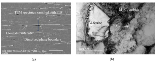
Figure 1.
Microstructure of Type 304L stainless steel containing δ-ferrite sensitized at 600 °C for four hours: (a) SEM micrograph after the DL-EPR test, showing elongated δ ferrite and partially dissolved phase boundary during the DL-EPR test; (b) TEM micrograph showing M23C6 carbide nucleated at the phase boundary.
The TEM specimen was harvested at the heavily dissolved phase boundary with FIB, as shown in Figure 1a. Figure 1b is a TEM micrograph showing parallel M23C6 carbides at the phase boundary between austenite and ferrite grains. Table 2 shows the chemical composition of major elements of ferrite, austenite and carbide measured with TEM-EDS. The Cr content is about 26 wt.% in ferrite and 18 wt.% in austenite, respectively. M in M23C6 is mainly composed of Cr and Fe. All the M23C6 carbides were nucleated at the phase boundary and grew into ferrite grain from the phase boundary. M23C6 carbides were not observed at the grain boundary between austenite grains in TEM, which is consistent with Figure 1a. All M23C6 grew from phase boundary to ferrite grain.

Table 2.
Chemical composition of major elements of the phases measured by TEM EDS in the AISI 304L stainless steel heat treated at 600 °C for four hours (in wt.%).
Figure 2a is a bright-field TEM image. Figure 2b shows SAED patterns of M23C6 carbide together with austenite. Figure 2c,d show ferrite and austenite, respectively. All of the micrographs in Figure 2 were obtained at B = [01] of M23C6 carbide. M23C6 has a face-centered cubic structure, as shown in Figure 2b. Every third spot in Figure 2b is very strong compared to the other spots and overlapping with that of austenite in Figure 2d, indicating that an OR between the austenite and M23C6 carbide exists. The OR is (111)a//(111)c and [10]a//[10]c, as described in previous works [7,10,22]. The lattice parameter of the carbide was about three-times that of the austenite. A comparison of Figure 2c with Figure 2d shows that the ferrite has no Kurjdjumov–Sachs (K–S) OR nor Nishiyama–Wassermann (N–W) OR with the austenite at the phase boundary. The K–S OR is (111)a//(110)f and [10]a//[11]f and the N–W OR is (111)a//(110)f and [10]a//[001]f [23]. SAED of ferrite (Figure 2c) was not observed at the beam direction of [110] of austenite, which suggests that neither K–S OR nor N–W OR exists between the austenite and the ferrite.
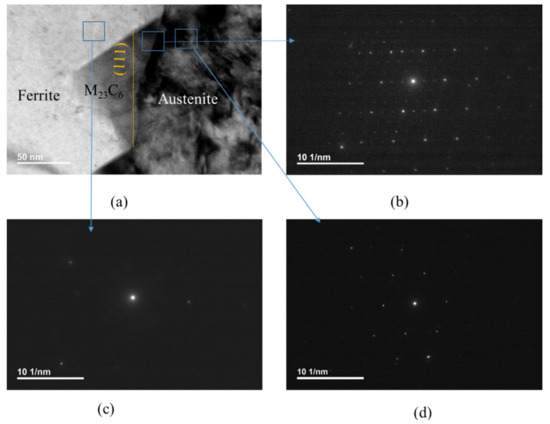
Figure 2.
TEM image and SAED pattern: (a) a bright-field TEM image; (b) SAED patterns of M23C6 carbide together with austenite; (c) SAED patterns of ferrite; (d) austenite. All micrographs were obtained at B = [01] of carbide.
The probability of the M23C6 establishing coherency with the ferrite is very low if the austenite has no coherency with the ferrite. A comparison of Figure 2b with Figure 2c shows that the δ ferrite has no OR with the M23C6 at the phase boundary, as expected from the absence of an OR between austenite and ferrite. The orange straight line in Figure 2a is the (111) plane in carbide. For carbide nucleated at the phase boundary between the austenite and ferrite grains, the phase boundary between the M23C6 and austenite is not at the (111) plane, nor is it macroscopically straight, as shown in Figure 2a, even though there is a coherency between austenite and the M23C6 grains. However, the edges of carbide nucleated at the phase boundary were parallel to those of the other carbides, as shown in Figure 1b. Both the coherency between austenite and the M23C6 grains and same orientation of edges of the M23C6 carbides at the phase boundary suggest that M23C6 nucleates at the (111) plane of austenite grain at phase boundary in the same manner that it nucleates at the (111) plane of grain boundary in fully austenitic stainless steel.
Based on our findings, M23C6 nucleation and growth models at the grain boundary and phase boundary are presented schematically in Figure 3. Figure 3a is a schematic diagram showing carbide nucleation at the (111) plane of austenite grain at the phase boundary. Figure 3b is a schematic diagram showing carbide growth at the phase boundary where the phase boundary between M23C6 and the austenite grains may change from the (111) plane of austenite to the other low-index plane of austenite with carbide growth. Apparently, the curved interphase interface between M23C6 and the austenite grain in Figure 2a might be a faceted interface, as shown in Figure 3b, on a smaller-length scale and consists of the (111) plane terrace connected by a low-index plane ledge, as suggested by previous works [23,24]. In fully austenitic stainless steel, M23C6 at the grain boundary has an OR with one of two austenite grains comprising the grain boundary and the coherent phase boundary between austenite and the M23C6 grains is the (111) plane because migration of the grain boundary just ahead of M23C6 takes places before M23C6 growth to minimize interfacial energy [10]. The interphase boundary between the M23C6 and austenite grain in austenitic stainless steel containing delta ferrite is rather severely curved, as shown in Figure 2a, whereas that in fully austenitic stainless steel is relatively straight [10]. The difference in interphase appearance may be attributed to the size of the atomic rearrangement zone around the boundary just ahead of the M23C6. The size of the atomic rearrangement zone in austenitic stainless steel containing delta ferrite may be much smaller than that in fully austenitic stainless steel because the carbide growth rate in austenitic stainless steel containing delta ferrite is faster than that in fully austenitic stainless steel due to higher chromium diffusivity in ferrite [21]. Carbide growth on the (111) plane of austenite grain in austenitic stainless steel containing delta ferrite may be most favorable if the other conditions are the same. However, if carbide growth on the (111) plane is not possible due to a smaller size of the rearrangement zone, then carbide growth may occur on the next favorable low-index plane, leading to a curved interphase boundary on the macro scale and faceted interphase boundary on the atomic scale.

Figure 3.
Schematic diagram of M23C6 nucleation and growth on phase boundary: (a) nucleation of M23C6 on (111) plane of γ boundary; (b) growth of the M23C6 on the migrating faceted phase boundary.
3.2. M23C6 Carbide Morphology at Phase Boundary
To examine the early-stage M23C6 carbide morphology, the following four steps were employed. Firstly, TEM images of carbide were obtained at various beam directions and then the angle between edges of carbide in the TEM image was measured. Secondly, a presumed carbide morphology was established based on the characteristics of M23C6 carbide at the grain boundary and then the angle between the edge of the image of the presumed carbide morphology was calculated at a given projection direction. Thirdly, the angle measured in the TEM image was compared with that calculated from the presumed carbide morphology. Fourthly, the presumed carbide morphology was modified until the angle measured in the TEM image matched that calculated from the presumed carbide morphology.
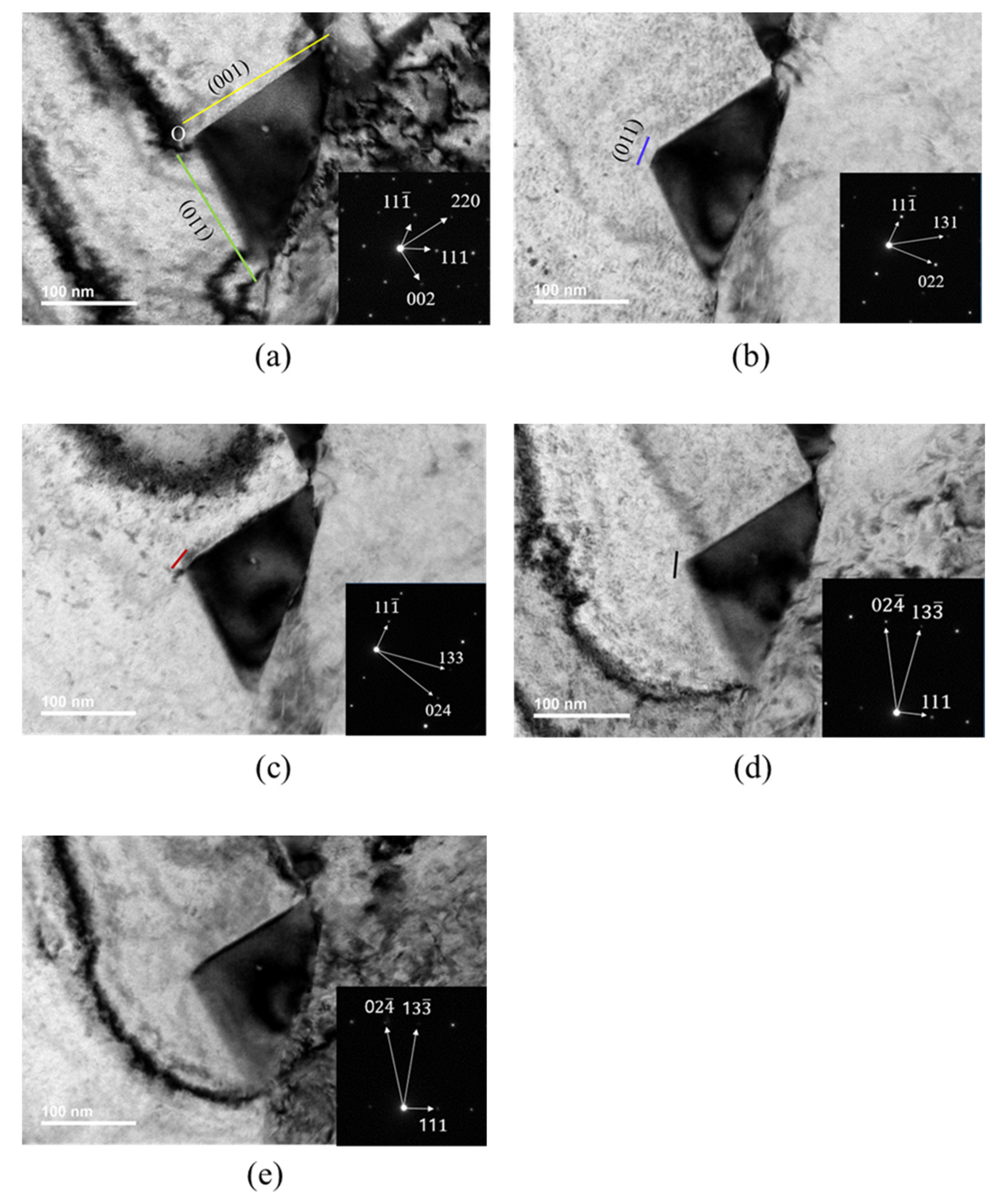
TEM images were taken at various rotation angles of the TEM specimen. Figure 4 shows TEM images and diffraction patterns obtained at B[10] (Figure 4a), B[21] (Figure 4b), B[31] (Figure 4c), B[21] (Figure 4d) and B[3] (Figure 4e). Diffraction patterns and TEM images at B[10] (Figure 4a) were obtained during rotation, either around the [111] pole or around [11]. The short red line in Figure 4c and short black line in Figure 4d were explained later in relation to carbide morphology.
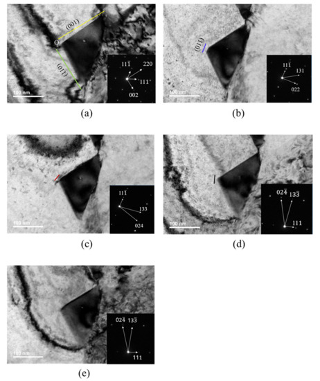
Figure 4.
TEM image and SAED of carbide with beam directions: (a) [10]; (b) [21]; (c) [31]; (d) [21]; (e) [3].
The M23C6 carbide at the grain boundary in fully austenitic stainless steel has the following characteristics. An OR exists between one of two austenite grains comprising the grain boundary and carbide, as in the matrix, i.e., (111)a//(111)c and [01]a//[01]c [7,10]. M23C6 carbide is partially bound by <110> segments on the (111) plane in the grain boundary [7], which is consistent with the OR between austenite and M23C6 carbide. The angle at the apex of the TEM carbide image is almost 90° in many cases when the TEM image is obtained at the <110> beam direction [10]. Faces of M23C6 carbide at the early stage are composed of low-index planes, as in type-3 incoherent boundaries [24]. The characteristics of the M23C6 carbide at the grain boundary in fully austenitic stainless steel may be applicable to those at the phase boundary between austenite and ferrite grains.
Figure 5 shows that M23C6 carbide morphology developed from (Figure 5a) to (Figure 5b) and finally to (Figure 5c). All capital letters except W in Figure 5 indicate vertex positions on carbide. W is a position on carbide such that WO parallels to QP. Figure 5a is an initially presumed M23C6 carbide morphology at the phase boundary because it has the characteristics of M23C6 carbide at the grain boundary in fully austenitic stainless steel. That is, the angle between edges of the image expected from Figure 5a is 90° for the <110> zone axis and the interfaces of Figure 5a are composed of low-index planes and carbide on the (111) basal plane is bound by the <110> segment. The fact that Figure 5a includes characteristics of M23C6 carbide at the phase boundary may not guarantee that Figure 5a is the real carbide morphology at the phase boundary. The feasibility of Figure 5a being the carbide morphology at the phase boundary was confirmed by comparing the angle measured between the edge in the TEM image and that calculated between edges in the image in Figure 5a in the beam direction.

Figure 5.
M23C6 carbide morphology at the phase boundary developed from (a) to (b) to finally (c) based on diffraction pattern and carbide angle in TEM image. Basal plane of the M23C6 carbide is the (111) plane.
The TEM image in Figure 4a was obtained at a beam direction of [10]. By comparing the diffraction pattern and carbide image in Figure 4a, the lower-side edge is almost parallel to the green line and the green line is perpendicular to the [220] direction in the SAED. The upper-side edge is almost parallel to the yellow line and the yellow line is perpendicular to the [002] direction in the SAED. Therefore, the lower-side edge almost parallel to the green line and the upper-side edge almost parallel to the yellow line were assigned to the (110) plane and the (001) plane, respectively. Then, the green line and yellow line in the TEM image in Figure 4a are consistent with the images generated by the BOA and COD interface in Figure 5a, respectively, at the beam direction of [10].
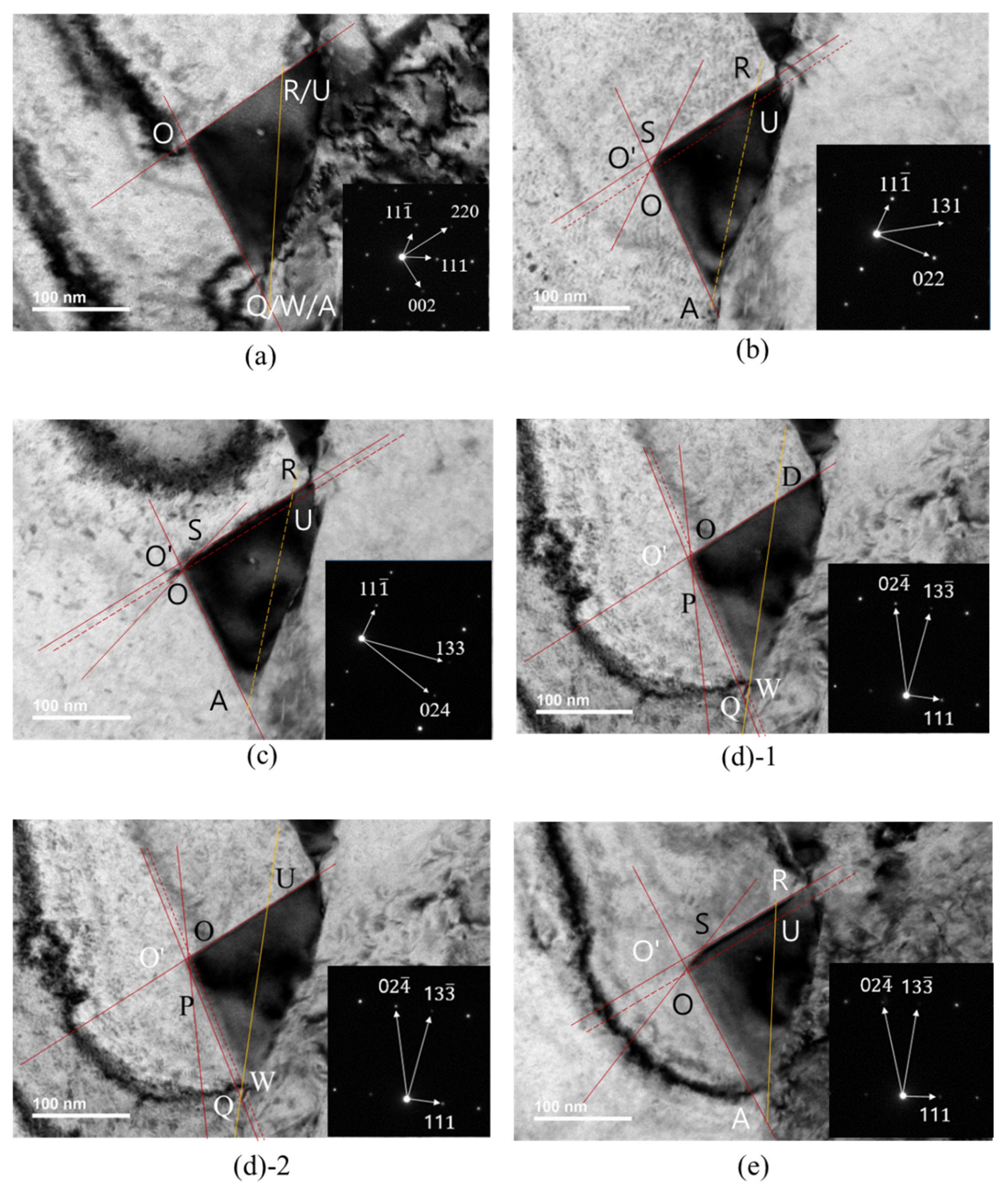
The TEM image in Figure 4b obtained at the [21] beam direction is a trapezoid. The edge of the TEM image parallel to the blue line in Figure 4b is perpendicular to the [022] direction of SAED at the [21] beam direction. Therefore, the edge parallel to the blue line was assigned to the (011) plane and is produced by BOC (011) in Figure 5a. However, the image expected from the carbide morphology in Figure 5a at the [21] beam direction is a triangular shape because the image is produced by the AOC in Figure 5a. The discrepancy between the TEM image in Figure 4b and the image expected from Figure 5a implies that the carbide morphology in Figure 5a is not valid. To obtain the trapezoid TEM image in Figure 4b, the carbide morphology was modified from Figure 5a to Figure 5b, where the QPSR (11) plane below the POS (011) plane in Figure 5b was additionally introduced because the QPSR (11) plane satisfies the characteristic of the M23C6. In this case, the edge of carbide parallel to the blue line in Figure 4b is produced by POS (011) in Figure 5b. Then, the image expected from the carbide morphology in Figure 5b at the [21] beam direction is a trapezoid and consistent with the TEM image in Figure 4b.
If we assign coordinates to the two vertex positions in Figure 5b, for example, O(111) and R( 1), then the coordinates of the other vertex positions are determined as shown in Table 3.

Table 3.
Coordinate of vertex positions on carbide in Figure 5.
Figure 6 is a duplication of Figure 4, with additional positions and lines corresponding to those in the carbide morphology in Figure 5 to avoid confusion in viewing the TEM carbide image in Figure 4. The position marked with a letter (for example, O) in the TEM image in Figure 6 corresponds to the position with the same letter (O) in the carbide morphology in Figure 5. Q, W and A coordinates in Figure 5c are given by one point in the TEM image of Figure 6a because the [10] beam direction is parallel to an edge, including Q, W and A coordinates in Figure 5c. R and U coordinates in Figure 5c are also given by one point in Figure 6a. Both Figure 6(d1,d2) corresponding to Figure 4d are the same, except the position mark D (Figure 6(d1)) and U (Figure 6(d2)). In Figure 6, the solid orange line is the (111) plane but the dotted orange line is not the (111) plane. The dotted orange line was drawn only to indicate coordinates of the position, where the (111) plane meets the other interfaces. ∠OSR in the TEM image in Figure 6b was measured and ∠OSR in the image expected from the carbide morphology in Figure 5b was calculated at the [21] beam direction. Both the angle measured and that calculated were 149°, which proves that the QPSR plane below the POS (011) plane in Figure 5b is the (11) plane. The trapezium TEM image in Figure 4c at the [31] beam direction is also generated by the AOSR of the carbide morphology in Figure 5b. The edge parallel to the short red line in Figure 4c is generated by the OS line in Figure 6b. O’ in Figure 6b corresponds to a position where extrapolation of AO and RS meet together in the TEM image.
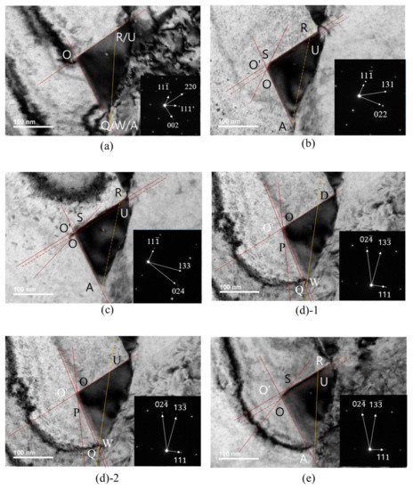
TEM images and SAED of carbide in Figure 4d,e were obtained at the [21] and [31] beam directions during rotation about the (111) pole, respectively. The edge parallel to the short black line in Figure 4d corresponds to of the carbide morphology in Figure 5b at the [21] beam direction. The TEM image of QPOD in Figure 6(d1) corresponds to the QPOD of carbide morphology in Figure 5b at the [21] beam direction. and are parallel to and , respectively, in Figure 5b. ∠QPO, ∠POD and ∠WOD in the TEM image in Figure 6(d1) correspond to ∠QPO, ∠POD and ∠WOD in the carbide morphology of Figure 5b at the [21] beam direction, respectively. ∠QPO, ∠POD and ∠WOD in the TEM image in Figure 6(d1) were measured and those for the carbide morphology in Figure 5b were calculated at the [21] beam direction. The results are listed in Table 4. ∠WOD is the same with ∠QO’D in the TEM image at the [21] beam direction in Figure 6(d1). ∠QPO measured in the TEM image in Figure 6(d1) closely matched that calculated from the carbide morphology in Figure 5b. However, ∠POD and ∠WOD measured in the TEM image in Figure 6(d1) deviate substantially from those calculated from the carbide morphology in Figure 5b, as shown in Table 4. The deviation in both ∠POD and ∠WOD measured in the TEM image from that calculated from the carbide morphology in Figure 5b means that Figure 5b is not real carbide morphology. If ∠POU and ∠WOU of the TEM image of carbide in Figure 6(d2) are generated by those of the carbide morphology in Figure 5c, then ∠POU and ∠WOU measured in the TEM image of carbide in Figure 6(d2) perfectly matches those calculated from the carbide morphology in Figure 5c, as shown in Table 4. Therefore, the initially presumed OSRD (001) plane in Figure 5b should be split to the (001) plane of OSRU and the unknown plane containing edge. Accordingly, the AOD (100) plane in Figure 5b should split to the (100) plane and the unknown plane. The unknown plane split from the OSRD (001) plane and that from the AOD (100) plane may be the same plane.

Table 4.
Comparison of the angle measured in TEM image and that calculated from carbide morphology at [21] beam direction.
Now, the carbide morphology at the right side of AOU in Figure 5c is identified completely but that at the left side of AOU remains. Interfaces of the carbide morphology at the left side of AOU may be assumed as low-index planes as in interfaces of the carbide morphology at the right side of AOU. Low-index planes with a [110] edge are the (11), (10), (001) and (11) planes. The (11) plane was excluded because the (11) plane with the [110] edge can not include the edge. The (001) plane was also excluded because the (001) plane was already there and could not make the [110] edge. The (10) plane was also excluded because the presence of the (10) plane does not allow for the (100) plane in Figure 5c. If the (10) plane exists, the (10) plane with edge also includes edge, that is, the (10) plane is AOV in Figure 5c. The (100) plane in contact with the OSP (011) plane in Figure 5c was confirmed in previous work [10]. Therefore, the possible unknown plane is the (11) plane. VOU (11) plane was introduced in Figure 5c. The (11) plane in Figure 5c is a reasonable choice in terms of a low-index plane and volume to surface energy ratio.
The presence of the edge in Figure 5c was not confirmed through a comparison of the angle measured with that calculated because TEM specimen rotation is limited. ∠WOV from the carbide morphology in Figure 5c for the beam direction of [10] was calculated to be 100°. The entire boundary at the basal plane of carbide is enclosed by <110> segments, which is consistent with the OR between austenite and carbide. Angles measured in the TEM image of Figure 6, except Figure 6(d1), closely match those calculated from the carbide morphology in Figure 5c at various beam directions, as shown in Table 5. Based on the findings and reasoning on the carbide morphology, the early-stage M23C6 carbide morphology is identified to be a complex pyramid shape in Figure 5c and is composed of low-index planes of {001}, {011} and {111} planes. Variants of Figure 5c produced by symmetry operations may be a morphology of the M23C6 at the phase boundary.

TEM images of intergranular M23C6 carbide were reported to be triangular and trapezoidal shapes in fully austenitic stainless steel [6]. These TEM images can be generated from just one kind of morphology, such as in Figure 5c. Care should be taken in inferring carbide morphology from TEM images because many TEM images can be generated by observing one kind of carbide morphology in different directions. However, the presence of other carbide morphology at the phase boundary cannot be ruled out. A prismatic morphology with a scalene quadrilateral cross-section was suggested as the carbide morphology, where the quadrilateral facets are the (11), (11), (02) and (200) planes, but the two end facets of the prismatic morphology were not identified [10]. If the M23C6 carbide morphology is a prismatic shape with a scalene quadrilateral cross-section and has the (111) basal plane, the TEM image will be changed from a triangle to a trapezoidal square when the beam direction is changed from B = [10] to B = [21] or to B = [3] for rotation around the [111] pole. However, the TEM image was not changed in that way in this work, as shown in Figure 4d,e. However, the presence of elongated pyramid morphology with a scalene quadrilateral cross-section may be possible in a later stage through preferential growth to the [01] direction in Figure 5c or coalescence of closely spaced carbides in Figure 5c.
3.3. Deviation in an Angle Measured from TEM Image from That Calculated from Carbide Morphology
The edge of a TEM carbide image is produced by either the face or edge of the carbide morphology at a given beam direction. If the face of carbide morphology includes the beam direction, the edge of the TEM carbide image is produced by the face of carbide; otherwise, it is produced by the edge of carbide morphology. For example, the (110) plane and (001) plane of carbide in Figure 5c includes the [10] beam direction and the (011) plane of carbide in Figure 5c also includes the [21] beam direction. In these cases, the edge of the TEM image is determined by the face of carbide morphology. At the [110] beam direction, OA and OU edges of the TEM carbide image in Figure 7a are produced by the (110) plane and (001) plane of carbide in Figure 5c, respectively. As shown in Table 5, angles measured in the TEM image matched well those calculated from the carbide morphology if the angle measured in the TEM image is determined by the edge of the carbide morphology. However, the former deviates slightly from the latter if determined by the face of the carbide morphology, as at the [10] beam direction. The deviation in between the measured and calculated value may be explained with a multilayer growth mechanism, as shown in Figure 7. The OA’ (green line) and OU’ (yellow line) in the TEM carbide image in Figure 7a are lines perpendicular to the [220] and [002] direction, respectively. OA of the carbide image deviates from OA’ by 5° and OU of the carbide image deviates from OU’ by 3° in Figure 7a at the [10] beam direction. Figure 7b,c are a three-dimensional view and side view of a schematic diagram, showing multilayer growth, respectively. Figure 7b shows that new carbide may nucleate above the growing carbide face before the growing carbide nuclei reach the edge of the face because of the high nucleation rate at the interior region of the face between the austenite grain boundary and carbide. If L is less than (v/Jo)1/3, multilayer growth is possible, where L is the dimension of the face, v is the nuclei growth rate and Jo is the nucleation rate [25]. That is, if the nucleation rate is faster than the growth rate then the angle measured in the TEM image will be larger than that calculated from ideal morphology.
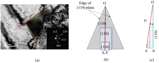
Figure 7.
Schematic diagram showing multilayer growth of M23C6 carbide on the (110) plane: (a) TEM image and diffraction pattern at the [10] beam direction where yellow and green lines are (001) and (110) planes, respectively, (b) three-dimensional view and (c) side view of multilayer growth of carbide on the (110) plane.
4. Conclusions
The early-stage M23C6 morphology at the phase boundary between δ ferrite and austenite in Type 304L austenitic stainless steel was investigated with TEM. The following conclusions were drawn.
- The M23C6 that nucleated at the phase boundary between ferrite and austenite has coherency with austenite. The phase boundary between the M23C6 and austenite grains has a curved appearance. The curved phase boundary might be a faceted interface composed of the (111) plane and the other low-index planes on the atomic scale.
- The M23C6 morphology at the phase boundary is identified to be a complex pyramidal shape that has {111}, {110} and {100} interfaces. Various shapes of TEM carbide images, such as triangular, scalene quadrilateral and trapezoidal shapes, can be generated from the M23C6 morphology, depending on the electron beam direction. Variants of the M23C6 morphology produced by symmetry operations may be a morphology of the M23C6 at the phase boundary.
- Angles measured in the TEM images agree well with those calculated from the carbide morphology when the former is determined from the edges of the carbide morphology. The former deviates slightly from the latter when the former is determined from the faces of the carbide morphology. The deviation may be attributed to multilayer growth in the interior region of the carbide face.
Author Contributions
Conceptualization, H.-P.K.; methodology, S.-Y.L. and Y.-S.L.; validation, M.-J.C.; formal analysis, H.-P.K.; investigation, H.-P.K., Y.-M.P. and H.-M.J.; resources, S.-Y.L.; data curation, S.-Y.L.; writing—original draft preparation, H.-P.K.; writing—review and editing, H.-P.K. and S.-W.K.; visualization, H.-P.K.; supervision, D.-J.K., S.-W.K. and S.-S.H.; project administration, M.-J.C.; funding acquisition, D.-J.K., S.-W.K. and S.-S.H. All authors have read and agreed to the published version of the manuscript.
Funding
This work was partly supported by the National Research Foundation of Korea (grant number: RS-2022-00143718 and 2021M2E4A1037979) and Korea Institute of Energy Technology Evaluation and Planning (grant number: 20191510301140), funded by the Korean government.
Institutional Review Board Statement
Not applicable.
Informed Consent Statement
Not applicable.
Data Availability Statement
The raw data required to reproduce these findings are available from the corresponding author on reasonable request.
Acknowledgments
The authors would like to acknowledge MS Ee-Soul Ryu at the TEM Laboratory for assistance.
Conflicts of Interest
The authors declare no conflict of interest.
References
- Cihal, V. Intergranular corrosion of steels and alloys. In Materials Science Monographs, 18; Elsevier: Amsterdam, The Netherlands, 1984; Volume 428, 500p. [Google Scholar] [CrossRef]
- Andresen, P.L.; Ford, F.P. Life prediction by mechanistic modeling and system monitoring of environmental cracking of iron and nickel alloys in aqueous systems. Mater. Sci. Eng. A 1988, 103, 167. [Google Scholar] [CrossRef]
- Stratulat, A.; Duff, J.A.; Marrow, T.J. Grain boundary structure and intergranular stress corrosion crack initiation in high temperature water of a thermally sensitised austenitic stainless steel, observed in situ. Corros. Sci. 2014, 85, 428. [Google Scholar] [CrossRef]
- Rahimi, S.; Marrow, T.J. A new method for predicting susceptibility of austenitic stainless steels to intergranular stress corrosion cracking. Mater. Des. 2020, 187, 1. [Google Scholar] [CrossRef]
- Lewis, M.H.; Hattersley, B. Precipitation of M23C6 in austenitic steels. Acta Metall. 1159, 13, 1965. [Google Scholar] [CrossRef]
- Singhal, L.K.; Martin, J.W. The Growth of M23C6 Carbide on grain boundaries in an austenitic stainless steel. Trans. Metall. Soc. AIME 1968, 242, 814. [Google Scholar]
- Adamson, J.P.; Martin, J.W. The nucleation of M23C6 carbide particles in the grain boundaries of an austenitic stainless steel. Acta Met. 1971, 19, 1015. [Google Scholar] [CrossRef]
- Terao, N.; Samal, B. Precipitation of M23C6 type carbide on twin boundaries in austenitic stainless steels. Metallography 1980, 13, 117. [Google Scholar] [CrossRef]
- Gao, M.; Wei, R.P. Precipitation of intragranular M23C6 carbides in a nickel alloy: Morphology and crystallographic feature. Scr. Met. 1994, 30, 1009. [Google Scholar] [CrossRef]
- Hong, H.U.; Rho, B.S.; Nam, S.W. Correlation of the M23C6 precipitation morphology with grain boundary characteristics in austenitic stainless steel. Mater. Sci. Eng. A 2001, 318, 285. [Google Scholar] [CrossRef]
- Kaneko, K.; Fukunaga, T.; Yamada, K.; Nakada, N.; Kikuchi, M.; Saghi, Z.; Barnard, J.S.; Midgley, P.A. Formation of M23C6-type precipitates and chromium-depleted zones in austenite stainless steel. Scr. Mater. 2011, 65, 509. [Google Scholar] [CrossRef]
- Maetz, J.Y.; Douillard, T.; Cazottes, S.; Verdu, C.; Kleber, X. M23C6 carbides and Cr2N nitrides in aged duplex stainless steel: A SEM, TEM and FIB tomography investigation. Micron 2016, 84, 43. [Google Scholar] [CrossRef]
- Stawström, C.; Hillert, M.J. An improved depleted-zone theory of intergranular corrosion of 18-8 stainless steel. Iron Steel Inst. 1969, 207, 77. [Google Scholar]
- Hall, E.L.; Briant, C.L. Chromium depletion in the vicinity of carbides in sensitized austenitic stainless steels. Metall. Trans. A 1984, 15, 793. [Google Scholar] [CrossRef]
- Was, G.S.; Kruger, R.M. A thermodynamic and kinetic basis for understanding chromium depletion in Ni-Cr-Fe alloys. Acta Metall. 1985, 33, 841. [Google Scholar] [CrossRef]
- Sourmail, T.C.; Too, H.; Bhadeshia, H.K.D.H. Sensitisation and Evolution of Chromium-depleted Zones in Fe-Cr-Ni-C Systems. ISIJ Int. 2003, 43, 1814. [Google Scholar] [CrossRef][Green Version]
- De Assis, K.S.; Rocha, A.C.; Margarit-Mattos, I.C.P.; Serra, F.A.S.; Mattos, O.R. Practical aspects on the use of on-site Double Loop Electrochemical Potentiodynamic Reactivation Technique (DL-EPR) for Duplex Stainless Steel. Corros. Sci. 2013, 74, 250. [Google Scholar] [CrossRef]
- Kauss, N.; Heyn, A.; Halle, T.; Rosemann, P. Detection of sensitisation on aged lean duplex stainless steel with different electrochemical methods. Electrochem. Acta 2019, 317, 17. [Google Scholar] [CrossRef]
- Plaut, R.L.; Herrera, C.; Escriba, D.M.; Rios, P.R.; Fediha, F. A Short review on wrought austenitic stainless steels at high temperatures: Processing, microstructure, properties and performance. Mat. Res. 2007, 10, 453. [Google Scholar] [CrossRef]
- Devine, T.M.J. Mechanism of Intergranular Corrosion and Pitting Corrosion of Austenitic and Duplex 308 Stainless Steel. Electrochem. Soc. 1979, 126, 374. [Google Scholar] [CrossRef]
- Williams, P.I.; Faulkner, R.G. Chemical volume diffusion coefficients for stainless steel corrosion studies. J. Mater. Sci. 1987, 22, 3537. [Google Scholar] [CrossRef]
- Redjaïmia, A.; Mateo, A. On the M23C6-Carbide in 2205 Duplex Stainless Steel: An Unexpected (M23C6/Austenite)—Eutectoid in the δ-Ferritic Matrix. Metals 2021, 11, 1340. [Google Scholar] [CrossRef]
- Headley, T.J.; Brooks, J.A. A new Bcc-Fcc orientation relationship observed between ferrite and austenite in solidification structures of steels. Metall. Mater. Trans. A 2002, 33, 5. [Google Scholar] [CrossRef]
- Massalski, T.B.; Soffa, W.A.; Laughlin, D.E. The nature and role of incoherent interphase interfaces in diffusional solid-solid phase transformations. Metall. Mater. Trans. A 2006, 37, 825. [Google Scholar] [CrossRef]
- Markov, I.V. Crystal Growth for Beginners: Fundamentals of Nucleation, Crystal Growth and Epitaxy; World Scientific: Singapore, 2016; ISBN 9789813104679. [Google Scholar]
Publisher’s Note: MDPI stays neutral with regard to jurisdictional claims in published maps and institutional affiliations. |
© 2022 by the authors. Licensee MDPI, Basel, Switzerland. This article is an open access article distributed under the terms and conditions of the Creative Commons Attribution (CC BY) license (https://creativecommons.org/licenses/by/4.0/).


