
Microstructure and Properties of Wire Arc Additive Manufacturing of Inconel 625

Abstract
:
1. Introduction
2. Materials and Methods
2.1. Materials
2.2. Deposition of Walls
2.3. Testing and Characterization
3. Results and Discussion
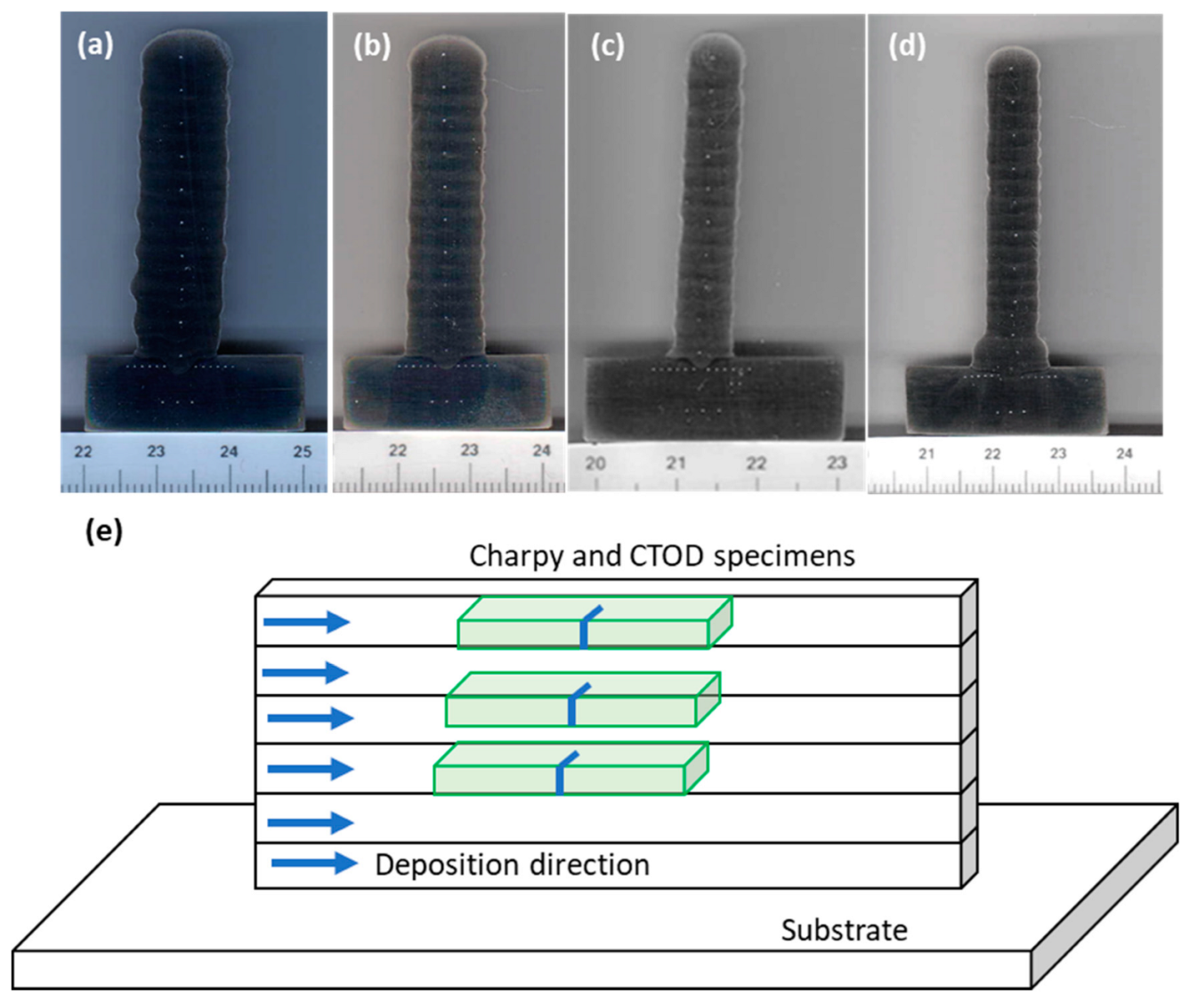
3.1. Macroscopic Examination
3.2. Hardness
3.3. Toughness
3.4. Optical Microscopy
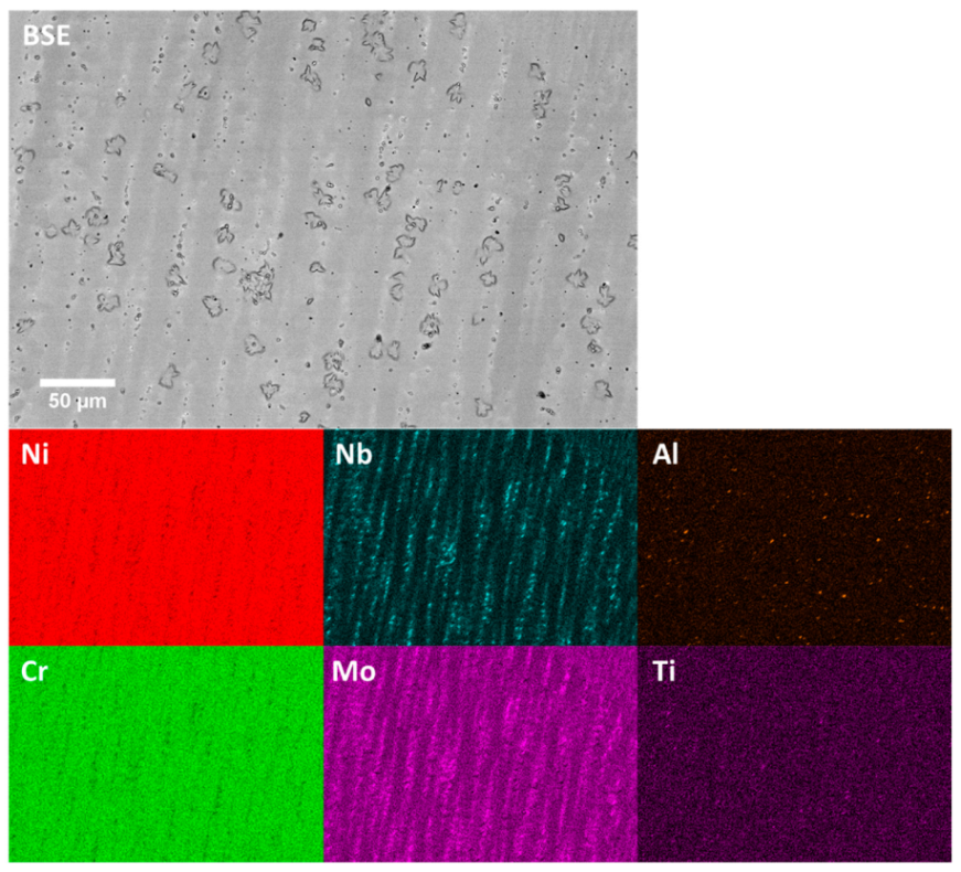
3.5. SEM and TEM Observations
4. Conclusions
- The hardness increases from the base metal level of 210, via the HAZ, with HV10 of 220, to the weld fused metal, with a hardness of around 240–250.
- The hardness was almost independent of the heat input within the current variation range.
- The Charpy V notch toughness was excellent, with variation between 160 and 200 J.
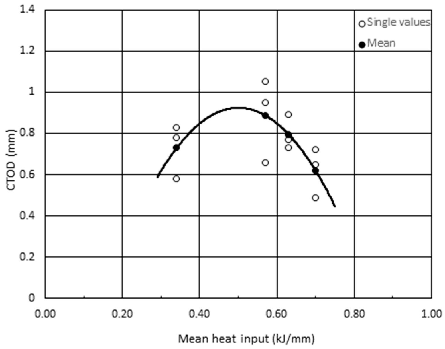
- The fracture toughness (CTOD) fell within a range of 0.49 to 1.05 mm.
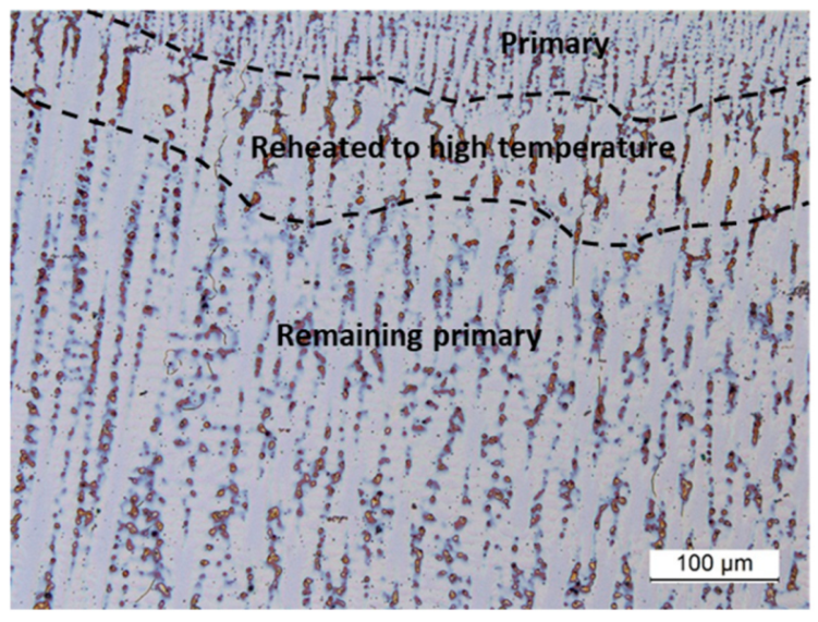
- Columnar dendritic solidification took place with heavy microsegregation of Mo and Nb to liquid interdendritic regions, and enrichment of Ni, Cr and possibly Fein primary dendrites.
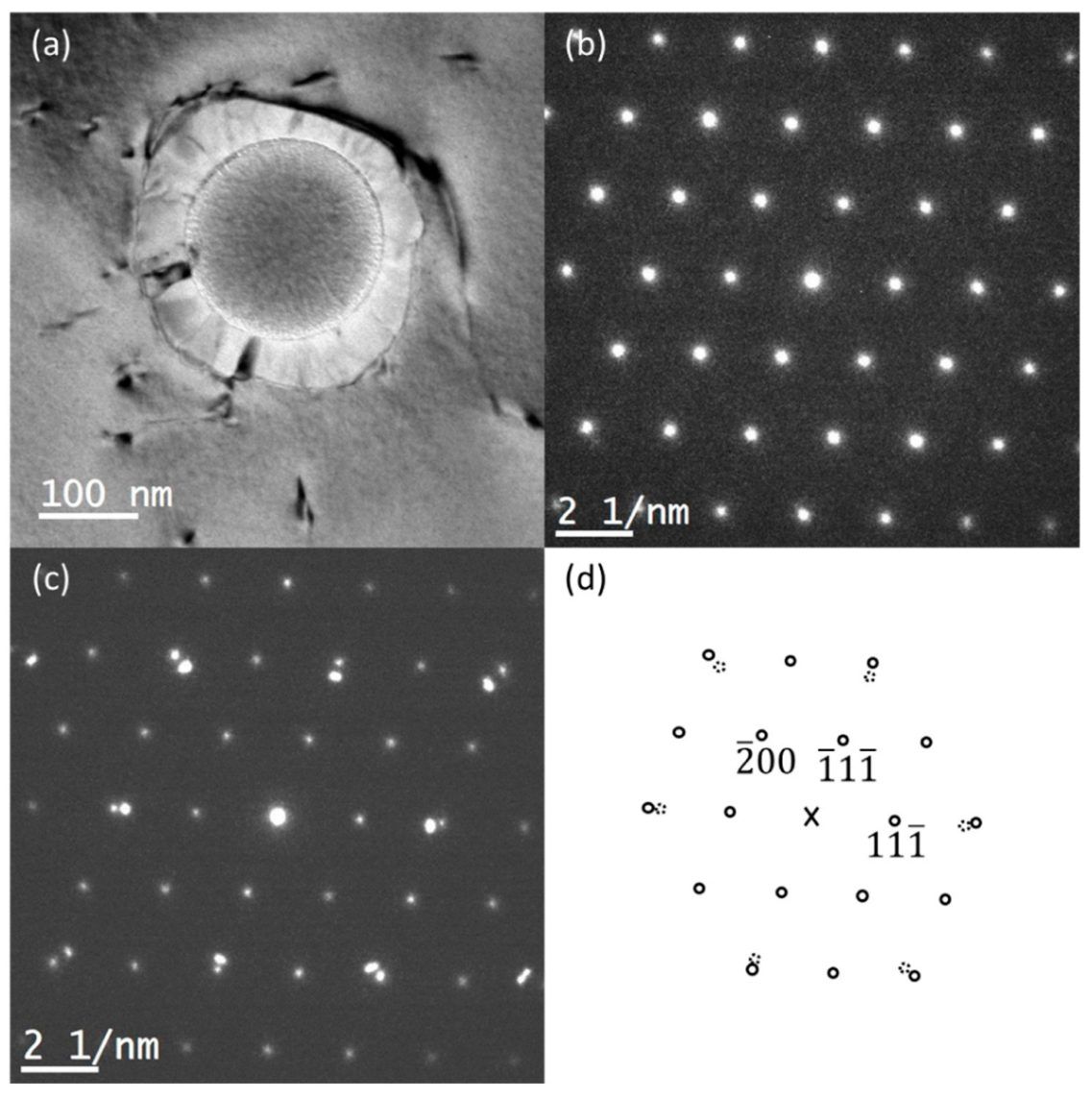
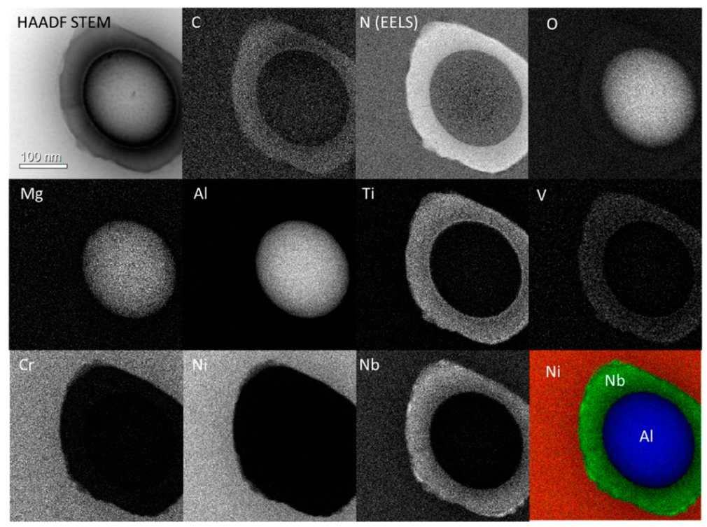
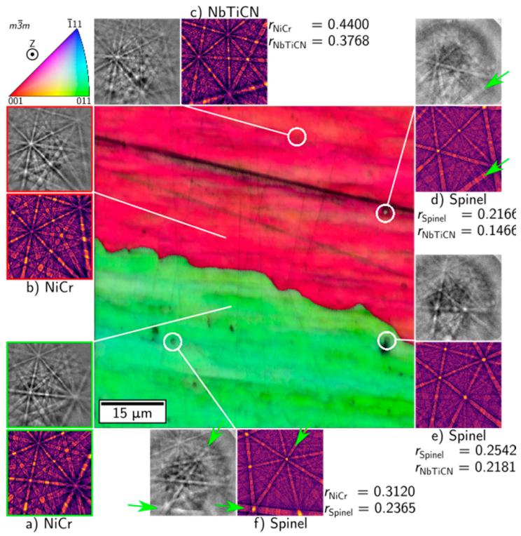
- Interdendritic regions contained particles like spinel (MgAl2O4). These were often surrounded by NbTiCN phase with the same orientation as spinel, suggesting that the interface between them is partially coherent.
Author Contributions
Funding
Institutional Review Board Statement
Informed Consent Statement
Data Availability Statement
Conflicts of Interest
References
- Martina, F.; Mehnen, J.; Williams, S.W.; Colegrove, P.; Wang, F. Investigation of the benefits of plasma deposition for the additive layer manufacture of Ti–6Al–4V. J. Mater. Process. Technol. 2012, 212, 1377–1386. [Google Scholar] [CrossRef] [Green Version]
- Szost, B.A.; Terzi, S.; Martina, F.; Boisselier, D.; Prytuliak, A.; Pirling, T.; Hofmann, M.; Jarvis, D.J. A comparative study of additive manufacturing techniques: Residual stress and microstructural analysis of CLAD and WAAM printed Ti–6Al–4V components. Mater. Des. 2016, 89, 559–567. [Google Scholar] [CrossRef] [Green Version]
- Williams, S.W.; Martina, F.; Addison, A.C.; Ding, J.; Pardal, G.; Colegrove, P. Wire plus Arc Additive Manufacturing. Mater. Sci. Technol. 2016, 32, 641–647. [Google Scholar] [CrossRef] [Green Version]
- ISO/ASTM 52900:2021; Additive Manufacturing—General Principles—Fundamentals and Vocabulary. International Organization for Standardization: Geneva, Switzerland, 2021.
- Fang, X.; Zhang, L.; Li, H.; Li, C.; Huang, K.; Lu, B. Microstructure Evolution and Mechanical Behavior of 2219 Aluminum Alloys Additively Fabricated by the Cold Metal Transfer Process. Materials 2018, 11, 812. [Google Scholar] [CrossRef] [PubMed] [Green Version]
- Fang, X.; Zhang, L.; Chen, G.; Dang, X.; Huang, K.; Wang, L.; Lu, B. Correlations between Microstructure Characteristics and Mechanical Properties in 5183 Aluminium Alloy Fabricated by Wire-Arc Additive Manufacturing with Different Arc Modes. Materials 2018, 11, 2075. [Google Scholar] [CrossRef] [Green Version]
- Cong, B.; Qi, Z.; Qi, B.; Sun, H.; Zhao, G.; Ding, J. A Comparative Study of Additively Manufactured Thin Wall and Block Structure with Al-6.3%Cu Alloy Using Cold Metal Transfer Process. Appl. Sci. 2017, 7, 275. [Google Scholar] [CrossRef] [Green Version]
- Cong, B.; Ding, J.; Williams, S. Effect of arc mode in cold metal transfer process on porosity of additively manufactured Al-6.3% Cu alloy. Int. J. Adv. Manuf. Technol. 2015, 76, 1593–1606. [Google Scholar] [CrossRef]
- Horgar, A.; Fostervoll, H.; Nyhus, B.; Ren, X.; Eriksson, M.; Akselsen, O.M. Additive manufacturing using WAAM with AA5183 wire. J. Mater. Process. Technol. 2018, 259, 68–74. [Google Scholar] [CrossRef]
- Wu, B.; Ding, D.; Pan, Z.; Cuiuri, D.; Li, H.; Han, J.; Fei, Z. Effects of heat accumulation on the arc characteristics and metal transfer behavior in Wire Arc Additive Manufacturing of Ti6Al4V. J. Mater. Process. Technol. 2017, 250, 304–312. [Google Scholar] [CrossRef]
- Martina, F.; Colegrove, P.A.; Williams, S.W.; Meyer, J. Microstructure of Interpass Rolled Wire + Arc Additive Manufacturing Ti-6Al-4V Components. Metall. Mater. Trans. A 2015, 46, 6103–6118. [Google Scholar] [CrossRef]
- Haden, C.V.; Zeng, G.; Carter, F.M.; Ruhl, C.; Krick, B.A.; Harlow, D.G. Wire and arc additive manufactured steel: Tensile and wear properties. Addit. Manuf. 2017, 16, 115–123. [Google Scholar] [CrossRef]
- Ji, L.; Lu, J.; Liu, C.; Jing, C.; Fan, H.; Ma, S. Microstructure and mechanical properties of 304 L steel fabricated by arc additive manufacturing. MATEC Web Conf. 2017, 128, 2017. [Google Scholar] [CrossRef] [Green Version]
- Rodriguez, N.; Vázquez, L.; Huarte, I.; Arruti, E.; Tabernero, I.; Alvarez, P. Wire and arc additive manufacturing: A comparison between CMT and TopTIG processes applied to stainless steel. Weld. World 2018, 62, 1083–1096. [Google Scholar] [CrossRef]
- Martina, F.; Ding, J.; Williams, S.; Caballero, A.; Pardal, G.; Quintino, L. Tandem metal inert gas process for high productivity wire arc additive manufacturing in stainless steel. Addit. Manuf. 2019, 25, 545–550. [Google Scholar] [CrossRef] [Green Version]
- Caballero, A.; Ding, J.; Ganguly, S.; Williams, S. Wire + Arc Additive Manufacture of 17-4 PH stainless steel: Effect of different processing conditions on microstructure, hardness, and tensile strength. J. Mater. Process. Technol. 2018, 268, 54–62. [Google Scholar] [CrossRef]
- Eriksson, M.; Lervik, M.; Sørensen, C.; Robertstad, A.; Brønstad, B.M.; Nyhus, B.; Aune, R.; Ren, X.; Akselsen, O.M. Additive manufacture of superduplex stainless steel using WAAM. MATEC Web Conf. 2018, 188, 03014. [Google Scholar] [CrossRef]
- Akselsen, O.M.; Bjørge, R.; Anes, H.W.; Ren, X.; Nyhus, B. Effect of Sigma Phase in Wire Arc Additive Manufacturing of Superduplex Stainless Steel. Metals 2021, 11, 2045. [Google Scholar] [CrossRef]
- Shankar, V.; Rao, K.B.S.; Mannan, S.L. Microstructure and mechanical properties of Inconel 625 superalloy. J. Nucl. Mater. 2001, 288, 222–232. [Google Scholar] [CrossRef]
- Shankar, V.; Valsan, M.; Rao, K.B.S.; Mannan, S.L. Effects of temperature and strain rate on tensile properties and activation energy for dynamic strain aging in alloy 625. Metall. Mater. Trans. 2004, 35A, 3129–3139. [Google Scholar] [CrossRef]
- Xu, F.; Lv, Y.; Liu, Y.; Shu, F.; He, P.; Xu, B. Microstructural evolution and mechanical properties of Inconel 625 alloy during pulsed plasma arc deposition process. J. Mater. Sci. Technol. 2013, 29, 480–488. [Google Scholar] [CrossRef]
- Asala, G.; Khan, A.K.; Andersson, J.; Ojo, O.A. Microstructural Analyses of ATI 718Plus® Produced by Wire-ARC Additive Manufacturing Process. Metall. Mater. Trans. 2017, 48A, 4211–4228. [Google Scholar] [CrossRef] [Green Version]
- Cozar, R.; Pineau, A. Morphology of γ′ and γ″ precipitates and thermal stability of Inconel 718 type alloys. Metall. Trans. 1973, 4, 47–59. [Google Scholar] [CrossRef]
- Xie, X.; Dong, J.; Wang, G.; You, W. The Effect of Nb, Ti, Al on Precipitation and Strengthening Behavior of 718 Type Superalloys. In Superalloys 718, 625, 706 and Derivatives; Loria, E.A., Ed.; TMS, The Minerals, Metals & Materials Society: Pittsburgh, PA, USA, 2005; pp. 287–298. [Google Scholar]
- Thivillon, L.; Bertrand, P.H.; Laget, B.; Smurov, I. Potential of direct metal deposition technology for manufacturing thick functionally graded coatings and parts for reactors components. J. Nucl. Mater. 2009, 385, 236–241. [Google Scholar] [CrossRef]
- Chen, Y.H.; Park, S.U.; Wei, D.; Newstadt, G.; Jackson, M.A.; Simmons, J.P.; de Graef, M.; Hero, A.O. A dictionary approach to electron backscatter diffraction indexing. Microsc. Microanal. 2015, 21, 739–752. [Google Scholar] [CrossRef] [PubMed]
- Ånes, H.W.; Natlandsmyr, O.; Bergh, T.; Lervik, L. Pyxem/Kikuchipy: Kikuchipy 0.4.0 (v0.4.0). Zenodo 2021. [Google Scholar] [CrossRef]
- Callahan, P.G.; de Graef, M. Dynamical Electron Backscatter Diffraction Patterns. Part I: Pattern Simulations. Microsc. Microanal. 2013, 19, 1255–1265. [Google Scholar] [CrossRef] [PubMed]
- Singh, S.; de Graef, M. Orientation sampling for dictionary-based diffraction pattern indexing methods. Model. Simul. Mater. Sci. Eng. 2016, 24, 085013. [Google Scholar] [CrossRef]
- Virtanen, P.; Gommers, R.; Oliphant, T.E.; Haberland, M.; Reddy, T.; Cournapeau, D.; Burovski, E.; Peterson, P.; Weckesser, W.; Bright, J.; et al. SciPy 1.0 Contributors: SciPy 1.0: Fundamental Algorithms for Scientific Computing in Python. Nat. Methods 2020, 17, 261–272. [Google Scholar] [CrossRef] [Green Version]
- Dinda, G.P.; Dasgupta, A.K.; Mazumder, J. Laser aided direct metal deposition of Inconel 625 superalloy: Microstructural evolution and thermal stability. Mater. Sci. Eng. 2009, A509, 98–104. [Google Scholar] [CrossRef]
- Wang, Y.; Chen, X.; Su, C. Microstructure and mechanical properties of Inconel 625 fabricated by wire-arc additive manufacturing. Surf. Coat. Technol. 2019, 374, 116–123. [Google Scholar]
- Korrapati, P.K.; Avasarala, V.K.; Bhushan, M.; Ramkumar, K.D.; Arivazhagan, N.; Narayanan, N.S. Assessment of Mechanical properties of PCGTA weldments of Inconel 625. Procedia Eng. 2014, 75, 9–13. [Google Scholar] [CrossRef]
- Xu, F.; Lv, Y.; Xu, B.; Liu, Y.; Shu, F.; He, P. Effect of Heat Treatment on Microstructure and Mechanical Properties of Inconel 625 Alloy Fabricated by Pulsed Plasma Arc Deposition. Phys. Procedia 2013, 50, 48–54. [Google Scholar] [CrossRef] [Green Version]
- Xu, F.; Lv, Y.; Liu, Y.; Xu, B.; He, P. Effect of deposition strategy on the microstructure and mechanical properties of Inconel 625 superalloy fabricated by pulsed plasma arc deposition. Mater. Des. 2013, 45, 446–455. [Google Scholar] [CrossRef]
- Wang, J.F.; Sun, Q.J.; Wang, H.; Liu, J.P.; Feng, J.C. Effect of location on microstructure and mechanical properties of additive layer manufactured Inconel 625 using gas tungsten arc welding. Mater. Sci. Eng. 2016, A676, 395–405. [Google Scholar] [CrossRef]
- Paul, C.P.; Ganesh, P.; Mishra, S.K.; Bhargava, P.; Negi, J.; Nath, A.K. Investigating laser rapid manufacturing for Inconel-625 components. Opt. Laser Technol. 2007, 39, 800–805. [Google Scholar] [CrossRef]
- Puppala, G.; Moitra, A.; Sathyanarayanan, S.; Kaul, R.; Sasikala, G.; Prasad, R.C.; Kukreja, L.M. Evaluation of fracture toughness and impact toughness of laser rapid manufactured Inconel-625 structures and their co-relation. Mater. Des. 2014, 59, 509–515. [Google Scholar] [CrossRef] [Green Version]
- Cam, G.; dos Santos, J.F.; Kocak, M. Properties of laser beam welded superalloys Inconel 625 and 718. In Proceedings of the European Conference on Laser Treatment of Materials, Hannover, Germany, 22–23 September 1998; pp. 333–338. [Google Scholar]
- Yeni, C.; Kocak, M. Fracture toughness analysis of laser-beam-welded super alloys Inconel 718 and 625. Fatigue Fract. Eng. Mater. Struct. 2006, 29, 546–557. [Google Scholar] [CrossRef]
- Floreen, S.; Fuchs, G.E.; Yang, W.J. The metallurgy of alloy 625. In Superalloys 718, 625, 706 and Various Derivatives; Loria, E.A., Ed.; TMS, The Minerals, Metals & Materials Society: Pittsburgh, PA, USA, 1994; pp. 13–37. [Google Scholar]
- ASM Metals Handbook Committee. ASM Metals Handbook. Properties and Selection: Nonferrous Alloys and Special-Purpose Materials, 9th ed.; ASM: Metals Park, OH, USA, 1980; Volume 3, p. 142. [Google Scholar]
- Yamanaka, T.; Takeuchi, Y. Order-disorder transition in MgAl2O4 spinel at high temperatures up to 1700 °C. Z. Krist. 1983, 165, 65–78. [Google Scholar] [CrossRef]
- Murphy, S.T.; Gilbert, C.A.; Smith, R.; Mitchell, T.E.; Grimes, R.W. Non-stoichiometry in MgAl2O4 spinel. Phil. Mag. 2010, 90, 1297–1305. [Google Scholar] [CrossRef]
- Kieffer, R.; Ettmayer, P.; Dufek, G.; Nowotny, H. Recent investigations on the miscibility of transition element nitrides and carbides. Metall 1972, 26, 701–708. [Google Scholar]
- Will, G.; Platzbecker, R. Crystal Structure and Electron Density Distribution in Niobium Carbide. Z. Anorg. Allg. Chem. 2001, 627, 2207–2210. [Google Scholar] [CrossRef]


| Ni | Cr | Mo | Fe | Nb | C | Mn | Si | P | S |
|---|---|---|---|---|---|---|---|---|---|
| >58.0 | 20.0–23.0 | 8.0–10.0 | < 5.0 | 3.15–4.15 | <0.10 | <0.50 | <0.50 | <0.015 | <0.015 |
| Parameter | Wall No. | ||
|---|---|---|---|
| W1 | W2 | W3 and W4 | |
| Current (A) | 231 | 201 | 139 |
| Voltage (V) | 21 | 20 | 17 |
| Travel speed (mm/s) | 7.0 | 7.0 | 7.0 |
| Wire speed (mm/s) | 12.7 | 10.3 | 6.7 |
| Heat input (kJ/mm) | 0.76 | 0.62 | 0.36 |
| Average interpass temperature (°C) | 152 | 140 | 85 |
| Polarity | DC+ | DC+ | DC+ |
| Wall Production Data | Wall No. | ||
|---|---|---|---|
| W1 | W2 | W3 and W4 | |
| Number of layers | 16 | 16 | 16 |
| Average layer height (mm) | 2.8 | 2.7 | 2.5 |
| Wall width (mm) | 11.8 | 10.2 | 7 |
| Wall length (mm) | 230 | 230 | 230 |
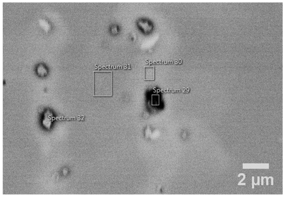
| Element/Spectrum | C | N | O | Mg | Al | Si | Ti | Cr | Fe | Ni | Nb | Mo |
|---|---|---|---|---|---|---|---|---|---|---|---|---|
| 29 | 26.9 | 7.2 | 25.0 | 5.5 | 12.4 | - | 3.4 | 4.1 | - | 7.7 | 6.9 | 1.0 |
| 30 | 25.4 | - | - | - | 0.3 | - | 0.3 | 18.8 | 0.2 | 45.9 | 4.0 | 5.1 |
| 31 | 26.0 | - | - | - | 0.1 | 0.3 | 0.2 | 19.7 | 0.2 | 47.5 | 1.7 | 3.8 |
| 32 | 46.2 | - | 16.0 | - | 0.9 | 0.1 | 2.7 | 5.7 | - | 11.8 | 14.9 | 1.7 |
| Element/ Spectrum | O | Mg | Al | Ti | Cr | Fe | Ni | Nb | Mo |
|---|---|---|---|---|---|---|---|---|---|
| 1 | - | - | - | 6.3 | 14.7 | 0.3 | 32.4 | 41.9 | 4.4 |
| 2 | 38.1 | 7.0 | 41.3 | 6.4 | 1.5 | - | 2.1 | 3.7 | - |
| 3 | 7.7 | - | - | 17.7 | 13.8 | - | 30.4 | 28.0 | 2.4 |
| 4 | 50.1 | 5.1 | 19.0 | 4.7 | 1.1 | - | 1.6 | 17.7 | 0.8 |
| 5 | 4.0 | - | - | 5.8 | 7.5 | - | 13.6 | 65.3 | 3.9 |
| 6 | - | - | - | - | 26.1 | 0.5 | 63.7 | 4.1 | 5.6 |
Publisher’s Note: MDPI stays neutral with regard to jurisdictional claims in published maps and institutional affiliations. |
© 2022 by the authors. Licensee MDPI, Basel, Switzerland. This article is an open access article distributed under the terms and conditions of the Creative Commons Attribution (CC BY) license (https://creativecommons.org/licenses/by/4.0/).
Share and Cite
Akselsen, O.M.; Bjørge, R.; Ånes, H.W.; Ren, X.; Nyhus, B. Microstructure and Properties of Wire Arc Additive Manufacturing of Inconel 625. Metals 2022, 12, 1867. https://doi.org/10.3390/met12111867
Akselsen OM, Bjørge R, Ånes HW, Ren X, Nyhus B. Microstructure and Properties of Wire Arc Additive Manufacturing of Inconel 625. Metals. 2022; 12(11):1867. https://doi.org/10.3390/met12111867
Chicago/Turabian StyleAkselsen, Odd M., Ruben Bjørge, Håkon Wiik Ånes, Xiaobo Ren, and Bård Nyhus. 2022. "Microstructure and Properties of Wire Arc Additive Manufacturing of Inconel 625" Metals 12, no. 11: 1867. https://doi.org/10.3390/met12111867