Article

An Improved Optimization Model to Predict the Deposition Rate and Smoothness of Ni Pulse-Reverse Electroplating Based on ANN and Experimental Results

by
Reza Ahmadian Koochaksaraie
1,
Farshad Barazandeh
2,* and
Mohammad Akbari
1
1
Micro-Technology-Lab, Mechanical Engineering Department, Amirkabir University of Technology, Tehran 15914, Iran
2
Mechanical Engineering Department, Amirkabir University of Technology, Tehran 15914, Iran
*
Author to whom correspondence should be addressed.
Metals 2023, 13(1), 37; https://doi.org/10.3390/met13010037
Submission received: 2 November 2022 / Revised: 19 December 2022 / Accepted: 19 December 2022 / Published: 23 December 2022
(This article belongs to the Special Issue Deposition, Dissolution, and Oxidation of Metals and Alloys)

Abstract

:
The metallic layers are an essential part of MEMS (micro electromechanical system) devices, and their deposition process must be accurately controlled; this may lead to difficulties as there are many input parameters for such a process. This research focuses on the input parameters’ effects on the Ni pulse-reverse electroplating. A neural network was constructed to characterize the pulse-reverse nickel electroforming process parameters. The sample training has accurately established the mapping relationship between input and output parameters. The nickel layer thickness and surface roughness prediction in the pulse-reverse electroplating process was realized and verified by experimental tests with a test error of 3.3%. Then, the effect of direct and reverse current density, deposition time, structure width, and stirring speed as input parameters on the thickness and surface roughness are investigated. Finally, a novel 4D diagram has been developed to derive the optimal values of direct and reverse current density relative to thickness, surface roughness, and deposition time. This diagram can help researchers and industries find suitable parameters to achieve the desired deposited Ni layer’s properties.

1. Introduction

The increasing need for smart devices has led to the growing use of micro-electro-mechanical devices. Two key features of these systems are the ability to be downsized and integrated. A successful MEMS (Micro Electro Mechanical systems) system uses these features to create unparalleled performance, increase reliability and sensitivity, and reduce costs [1].
MEMS technology integrates microelements such as sensors, actuators, and electronic devices by using microfabrication technology [2,3]. These systems are generally fabricated by micromachining processes which deposit new layers on the substrate and selectively etch portions of the silicon wafer or deposit layer to form the mechanical and electromechanical components of the system. However, various physical and chemical processes used in the microfabrication of MEMS devices can make it difficult to manufacture reliable structures. High temperatures and extreme pressure conditions generally cause deformations and changes in the microstructure’s material properties that can result in various physical conditions and chemical reactions [4,5].
Most current MEMS devices use polysilicon, made by chemical vapor deposition (CVD), as a structural material. However, silicon-based technologies are not suitable for many applications that require a thick layer of metal or alloy as a part of the structures. In contrast, LIGA (German acronym for lithography, electroplating, and molding) technology, based on UV lithography, offers considerable advantages. It can fabricate metal and alloy layers up to several hundred or thousands of microns thick with great precision [6].
Electrodeposition is widely used to fabricate micro-components and micro-structures in electronic devices. In addition, the fabrication of microstructures by photolithography and electroplating is attracting attention in developing MEMS devices using metals [7,8]. Electroplated nickel is commonly used to fabricate complicated surfaces and 3D materials that require precise dimensional tolerance. It is suitable in applications where a high film growth rate, defect-free structure, high mechanical strength, high-aspect ratio, and uniform film thickness distribution are critical [9].
There are many examples of microfabricated complex MEMS structures using an electroplated Ni layer employing the LIGA/UV-LIGA process. In 2005, J. Luo et al. developed an electrothermal micro tweezer for micromanipulation with an electroplated nickel structural layer on the Cr/Cu seed layer and Si sacrificial substrate [10]. Guannan Liu et al. fabricated a micro-heater for aerosol generation applications by e-beam evaporation and solution-based nickel plating on an amorphous silicon membrane [11]. Later in 2017, S. Sun et al. presented an electromagnetic energy harvester with an electroplated nickel layer and backside etching of the silicon substrate [12]. Moreover, a MEMS triboelectric energy harvester and the sensor were presented by Hamid, H.A., and Z. Çelik-Butler using the UV-LIGA technique employing electroplated nickel in 2020 [13].
The mechanical properties of electroplated materials are generally different from bulk materials. The reason for these differences in properties is that the microstructure (grain size, porosity, etc.) of these components made by the LIGA technique often depends on the plating conditions of the layer (direct, pulse, or pulse-reverse current electroplating) [14]. In this regard, electroplated nickel residual stress [8], fracture toughness [15], morphology, average grain size, hardness, micro-mechanical property, and thickness distribution [9] have been developed as the output factors of the electroplating process.
Among these researches, the missed factor is that the surface roughness and deposition rate for the process in various conditions had not been covered thoroughly. So one cannot use single research to obtain the process parameters to achieve the desired result on the deposited layer.
Surface roughness affects capacitance in RF-MEMS switches [16] and the adhesion forces of MEMS surfaces [17]. Furthermore, surface roughness could be related to the fatigue properties of electroplated nickel in MEMS applications [18]. Therefore, it is vital to know the surface roughness of nickel-plated microstructures if they are to be used for any commercial application.
Generally, in the electroplating process, temperature, deposition time, current density, reverse current density, metal type, pH value, stirring speed, and solution concentration are the input parameters that control and modify the output parameters (deposition rate, grain size, surface roughness, and adhesion) of the deposited layer.
The current fluctuates rapidly between two different values in the pulse-reverse electroplating process. Pulse parameters, including duration, amplitude, and polarity, are shown in Figure 1.
The pulsed reverse current technique interrupts the coating step, and a peel time is introduced into the cycle to selectively dissolve the protrusions of the metal surface and ensure a uniform surface. The reverse pulse current has the advantages of the pulse current technique. It can result in better surface roughness, ductility, and electrical conductivity since it needs less additive than the pulse one when a high-frequency pulse is applied [14].
A fundamental feature of the pulse deposition technique is modifying the diffused layer. Under pulse deposition conditions, the concentration line slope is reduced, and more ions are placed on the cathode area, which increases the deposition rate [19]. Moreover, pulsed deposition techniques are mainly used to improve the current distribution and shininess of the deposited layer [20]. An advantage of pulse-reverse current electroplating over pulse current form is the roughness and uniformity of the surface. By varying the polarity, the roughness in the pulse-reverse is permanently reduced, and the quality and uniformity of the surface are improved. Negative pulses in pulsed electroplating result in selective solubility and remove excess materials from areas where charge density has accumulated (such as sharp edges) [21,22].
In this research, the experimental setup, including the specimen preparation steps, design of experiments, and measurement methods, will be explained. Next, the NN modeling will be introduced, and the results will be presented and discussed in the final section.

2. Experimental Setup

2.1. Microfabrication Process

The fabrication procedure is based on UV-LIGA technology, shown in Figure 2. At first, chrome and gold are deposited on the substrate as the adhesion and seed layers via sputtering by ACECR Sharif University of Technology Microelectronics Lab. The gold layer has a suitable adhesion property to both chrome and nickel layers; On the other hand, it acts as a perfect conductor of electrical current and is expected to lead the process to desired results in the nickel electrodeposition.
In the next step, photolithography is used to pattern the samples on the wafer. The specimens are immersed in acetone and alcohol for 6 to 10 min to prepare the gold surface for coating. After this step, the sample is dehydrated for 3 min by baking at 100 °C to remove moisture from its surface. Initially, a thin layer of Hexamethyldisilazane (HMDS) solution is coated on the surface of the samples by the spinner for better photoresist adhesion to the gold layer. The negative photoresist used for this purpose is KMPR 1025 by Microchem. This photoresist is suitable for high-thickness coating and can easily be stripped after the electrodeposition step.
After the photolithography process, the electrodeposition begins. A pulse-reverse power supply by Plating Electronic® (Sexau, Germany) was employed to generate the desired pulse-reverse current.
Details of the fabrication process are as follows:
  • One-sided oxide silicon wafers are selected as the substrate.
  • RCA1 cleaning for 3 min to remove contaminants.
  • RCA2 cleaning for 3 min.
  • Deeping in deionized water for 3 min.
  • Washing wafer with water and drying with nitrogen.
  • SiO2 passivation layer etching.
  • Cr adhesive layer deposition by sputtering (50 nm).
  • Au conductive layer deposition by sputtering (150 nm).
  • Cleaning with acetone and IPA.
  • KMPR photolithography by UV- exposure.
  • Ni structural layer deposition by pulse-reverse electroplating.
  • Photoresist stripping.

2.2. Design of Experiments

The experiments were performed by combining different input parameters of the nickel pulse electrochemical coating process to evaluate the thickness and surface roughness of the pulse-reverse electroplated nickel layer. These parameters were selected regarding the usual values in the prior research or MEMS structure’s dimensional properties. This study considers the ratio of reverse to direct current (RTD) 2, 3, and 4. Moreover, the current density is considered in the range of 10, 20, and 30 mA/cm2. A magnetic stirring bar at 110, 220, and 330 rpm was implemented to ensure the homogeneity of the electrolyte during the deposition process. Layer thickness and surface roughness were evaluated after 10, 30, and 60 min of deposition (to achieve the thickness of the layer usually used in MEMS structures); finally, a total of 81 experiments were obtained. The sulfamate bath composition was 100 g/L Ni(SO4NH2)2, 10 g/L NiCl, 0.8 g/L SDS (Sodium dodecyl sulfate) and 40 g/L H3BO3, and the bath temperature was 45 °C.
An attempt was made to increase the number of experiments and the data to improve the neural network’s prediction accuracy. So the specimens used in tests included channels with dimensions of 1 mm in the length of 40, 50, and 60 μm (the width of the channels is considered to be in this range, so the aspect ratio remains lower than 1). Finally, the factorial experimental design is determined using Minitab® V.21 software by considering a total of 243 test specimens (81 sets of data related to electroplating parameters and three sets related to electroplated channel dimensions) to evaluate and predict the thickness and surface roughness under different electroplating conditions.

2.3. Surface Roughness and Layer Thickness Measurement Method

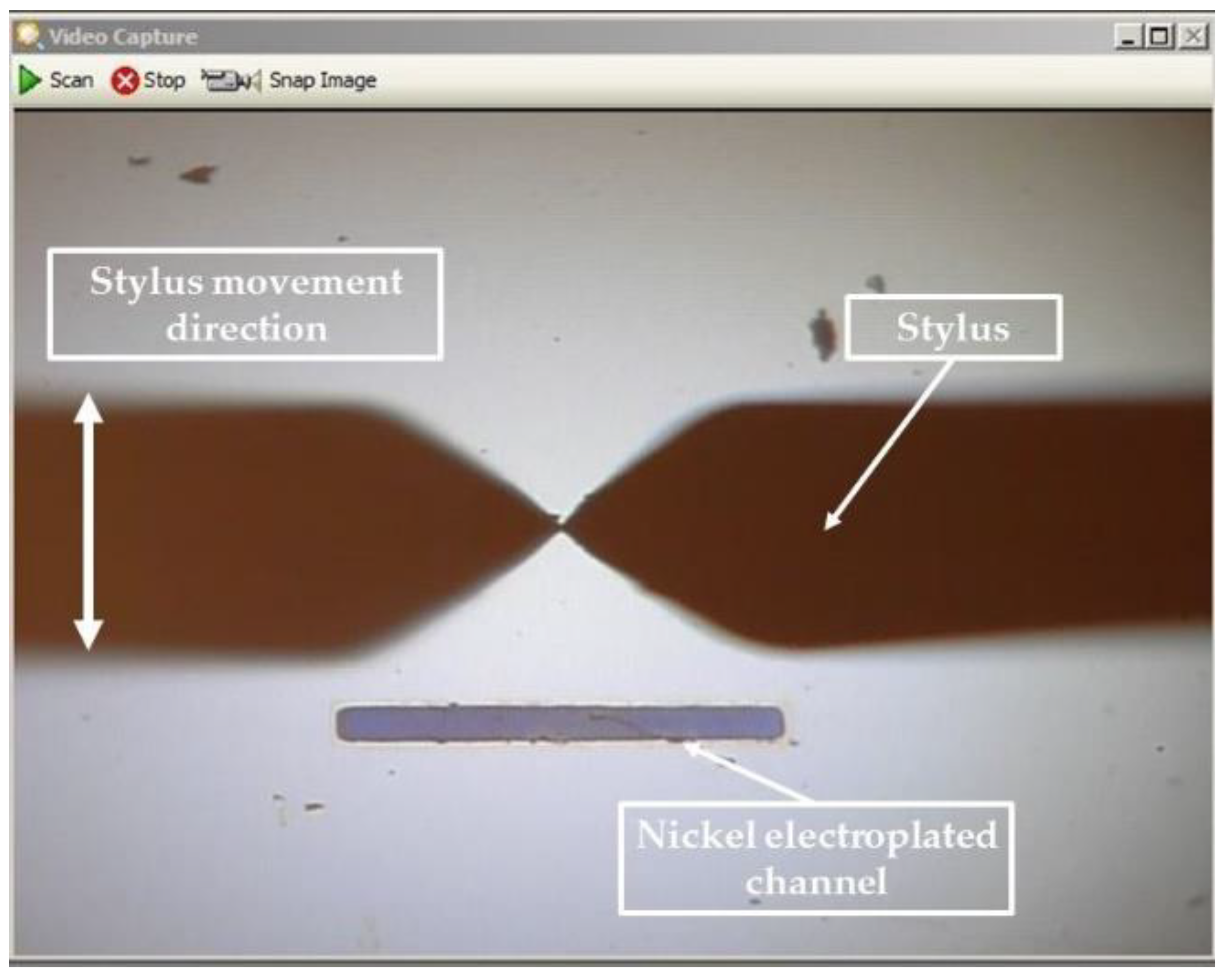
A contact profilometer (AlphaStep® D-100 stylus profiler, Milpitas, CA, USA) examined the surface roughness and thickness of the nickel layer. In this way, the specimen is placed on the stage of the profilometer after stripping the photoresist. As shown in Figure 3, a stylus in a typical contact position moves laterally from the starting point of the substrate along the width of the electroplated nickel channel for a certain distance and records changes in the height of the stylus. As a result, the thickness of the nickel layer can be measured by measuring the height changes between the substrate and the nickel surface. Furthermore, the arithmetical mean deviation of the profile (Ra) is calculated as the surface roughness on the nickel layer’s top surface (Figure 4).

3. Neural Network Modeling

Artificial Neural Networks (ANN) is a simple, robust, nonlinear modeling tool that can predict and generalize experimental tests, for example, optimizing copper electroforming process parameters [23]. It uses many connections between its processing blocks as neurons. Neurons’ act is based on training patterns, inputs, and forecasting outputs. So to characterize the surface roughness and thickness of the nickel layer based on experimental results, the neural network box of MATLAB® V.2020a was used.
There are two types of artificial neural networks, the “feed-forward” and the “feed-back” network. Since the feed-forward network is more useful in nonlinear transformation, this method has been employed. The number of neurons’ input and output layers equals the input and output parameters. The number of neurons in hidden layers depends on the complexity of the problem. There is no straightforward way to determine the minimum required neurons, and this number is usually assigned by trial and error.
Figure 5 shows the feed-forward ANN configuration used to predict the surface roughness and thickness of the nickel layer. This configuration included three layers (the input layer, one hidden layer, and the output layer) with five input neurons, the hidden neurons, and two output neurons. The deposition time, the rotational speed of the stirrer, direct current density, RTD, and the channel width are input neurons. The nickel layer thickness and surface roughness are considered the output neurons.
For modeling the feed-forward ANN, the Sigmoid function is used as the transfer function for hidden layers (Equation (1)).
f(net) = 1/(1 + e−x)
The data range for the Sigmoid function is (−1, 1), and the input data is normalized by Equation (2) [24,25].
d = 0.8 × ((x − xmin)/(xmax − xmin)) + 0.1
where xmin and xmax are the minima and maxima quantity of each input data, this function maps input to the normalized parameter (d) in the (0.1, 0.9) range.
The learning algorithm in this study is a backpropagation error. The mean squares of error (MSE) are employed to evaluate the neural network training accuracy following (Equation (3)) [26]:
M S E = i = 1 n ( x i x ¯ ) 2 n
where n is the number of the test data.

Layer’s Thickness and Surface Roughness Prediction Using NN

The neural network training aims to estimate the output values (surface roughness and layer thickness) based on the input parameters’ value. Among the 223 sets of data related to the tests, 219 were considered for network training, and 24 were considered for evaluating the trained network. Network training was performed with the different numbers of hidden layer neurons, and the results are compared in Table 1. It is observed that the 3% value of MSE and the 0.7% absolute mean of training data error occur in a network with seven hidden layer neurons, so one is the candidate for NN modeling.
Figure 6a compares the results of ANN prediction and the actual results of the 24 check data sets. It can be concluded that the obtained surface roughness results of the experiments can verify the neural network prediction. Similarly, Figure 6b shows the high accuracy of the neural network in predicting the thickness of the nickel layer and can model the effect of the pulse-reverse electroplating process input parameters on the deposition rate and surface roughness.

4. Results and Discussion

4.1. The Effect of the Beam Width on the Layer Thickness and Surface Roughness

Beams are used in electromechanical devices such as microgrippers and accelerometers. The designed beam width depends on the device’s performance [27]. The lithography of a channel creates beams in the UV-LIGA fabrication method. They are being filled with a deposited metallic layer. Therefore, the effect of the beam width on the deposition rate and smoothness is concerned with nickel electroplating.
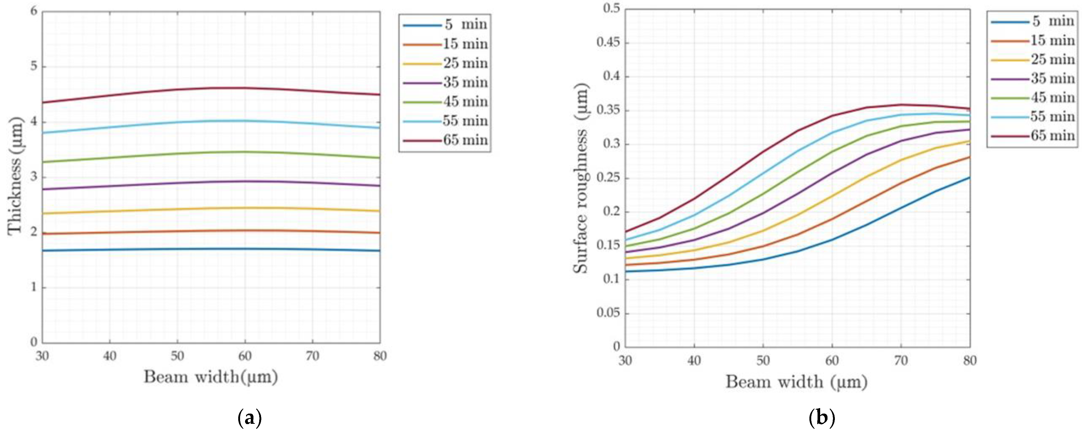
The resulting layer thickness, surface roughness, and beam width relation were plotted in Figure 7. Regarding Figure 7a, it can be observed that the thickness growth rate is linear and roughly constant with a change in beam width in the case of increased beam width. Nevertheless, it can be seen from Figure 7b that surface roughness grows with an increase in the beam width, and it should be considered in the design of wide beams. Notice that this concept rules for aspect ratios lower than 1, and for those higher than 1, it may be different [21].

4.2. The Effect of Stirring Speed on the Layer’s Thickness and Surface Roughness

As Figure 8a shows, increasing the stirring speed will increase the overall layer’s thickness to an optimum, and then the thickness drops. Moreover, the optimum stirring speed rises slightly with increasing deposition time. Therefore, the optimal value in 5 and 65 min is 155 and 180 rpm, respectively, which shows the maximum nickel thickness relative to the stirring speed. The drop in the layer’s thickness when moving away from the optimum value is due to the increased speed of metallic ions, which prevents them from being attracted by the cathode [28]. Likewise, according to Figure 8b, the optimal value of the minimum surface roughness in the defined range for the stirring speed is observed. The optimal stirring speed for the best surface roughness decreases from 220 to 110 rpm for 5 to 65 min of deposition.

4.3. The Effect of RTD on the Layer Thickness and Surface Roughness

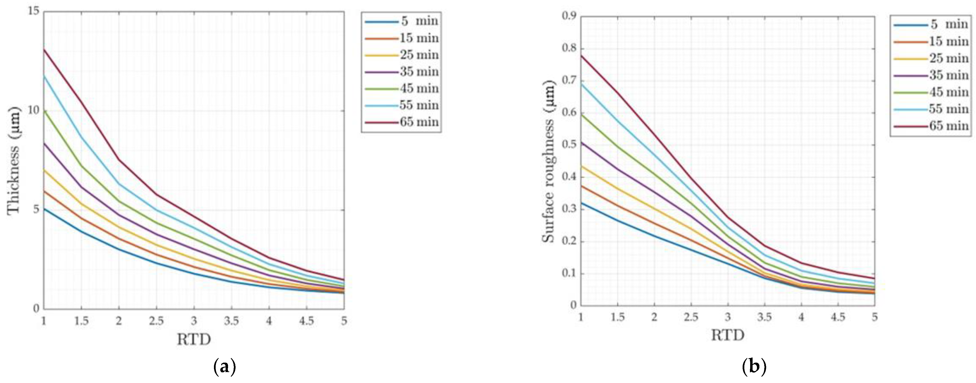
Figure 9a shows that the layer thickness decreases with increasing the RTD. This phenomenon is due to an increased under-the-curve area ratio of the applied current diagram (reverse current vs. direct current). As this ratio increases, the material pick-up from the part does the same. Therefore, the obtained thickness is less under the same conditions, and the thickness reduction rate decreases with increasing the RTD.
On the other hand, Figure 9b shows that the surface roughness improves when RTD increases. The ratio has a drastic effect on surface quality with a high ramp. Moreover, by increasing the deposition time, the changes are more severe related to the sum of the area under the current-time curve diagram. Increasing RTD would give the reverse circuit more opportunities to reduce surface roughness.
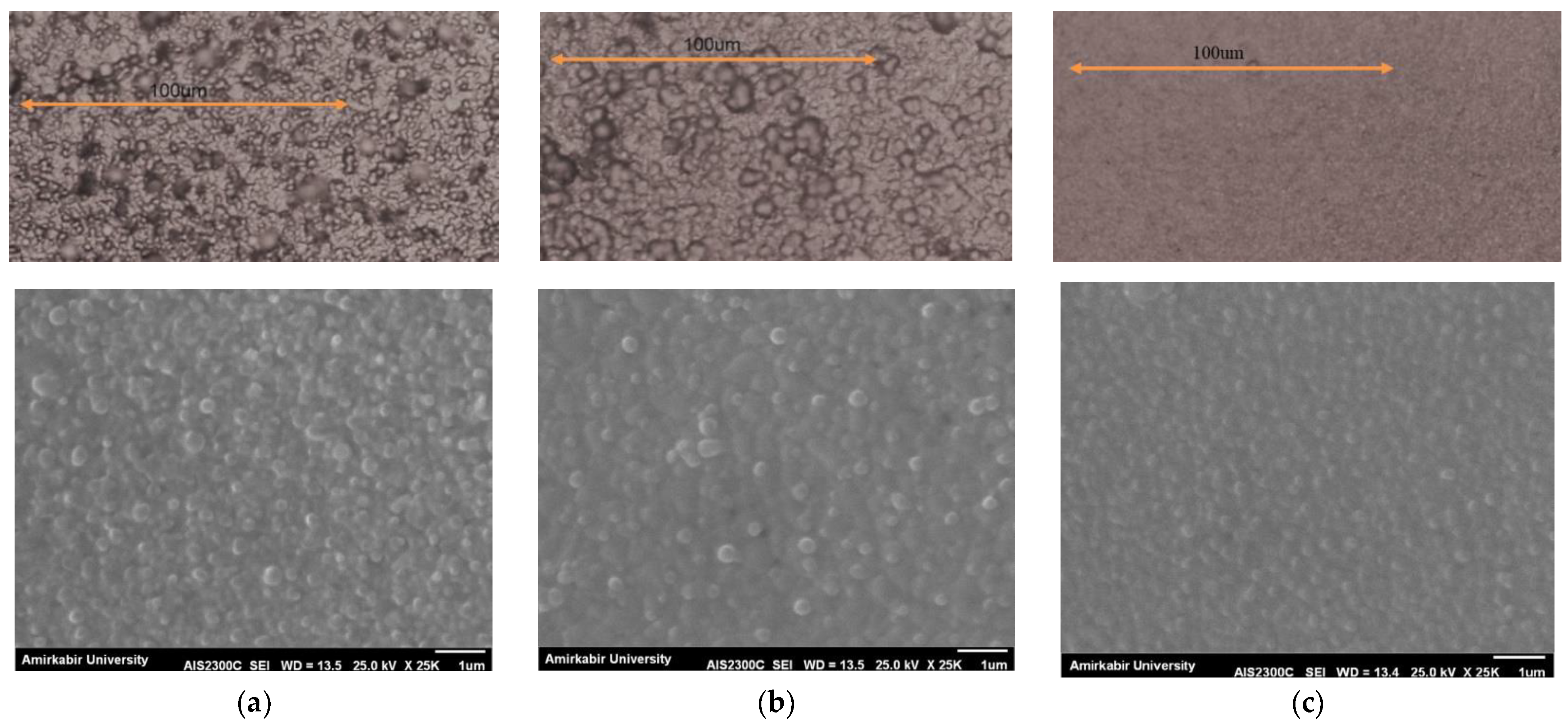
In another evaluation, Figure 10 shows optical and scanning electron microscope (SEM) images of three deposited nickel layers with a current density of 20 mA/cm2 and RTD of 2, 3, and 4. As stated in [29], the grain size increases when the RTD decreases. It is because increasing the reverse current density increases the time of the reverse current connected in the circuit. Therefore, it does not allow nickel grains to grow.

4.4. The Effect of Current Density on the Layer Thickness and Surface Roughness

Luo et al. investigated the deposition conditions on the layer’s properties [10]. Their research results for a current density of 30 mA/cm2 was 10–25 nm in surface roughness and a rate of approximately 5.2 µm/min deposition rate. Tseluikin et al. studied the effect of several parameters on nickel-based composites [30]. The results verified the prior works and showed that the surface roughness of the layer increases b increasing the current density.
The relationship between the current density and layer thickness of the deposited layer for the current is shown in Figure 11a. Generally, the deposition rate of the nickel layer increased with an increase in the current density. However, a remarkable layer deposition rate variation was not observed when the current density was changed from 5 to 15 mA/cm2. The rate increased substantially with the increase in the current density from 15 to 25 mA/cm2. According to cathode efficiency, the high cathode current efficiency describes that most of the energy applied to the plating cell is used for metal deposition and not wasted during reactions such as hydrogen evolution. So, at low current densities with reduction, the cathode efficiency reduces the deposition rate [31]. Moreover, the layer’s thickness deviation decreases for current densities up to 25 mA/cm2 due to approaching the current limit density [21].
In addition, the results of surface roughness relative to current density are shown in Figure 11b. Behavioral change of surface roughness is similar to those in deposition rate. The surface roughness changes are negligible with increased current density from 5 to 15 mA/cm2. Increasing the current density from 15 to 25 mA/cm2 increases surface roughness. The surface roughness variation decreases in the current density greater than 25 mA/cm2.

4.5. Optimization and Adjustment of Parameters for Nickel Pulse-Reverse Electroplating

The results in the above section show that the beam width parameter has a more negligible effect on the thickness and smoothness of the nickel layer than the other parameters. The stirring speed also has an optimal range based on the result. Nevertheless, regarding the changes in RTD and current density, there would be no specific optimal sets of these two input parameters to achieve optimal deposited layer thickness and surface roughness.
Therefore, to identify the range of parameters in which the thickness and surface roughness are within the desired range of the microfabrication process, the average beam width of 50 μm and the stirring speed of 180 rpm were adjusted. Furthermore, RTD and current density during the deposition time, relative to the surface roughness and layer thickness, are examined simultaneously the 4D diagram presented in Figure 12.
The distinctive feature of this 4D diagram is the simultaneous interpretation of the thickness and surface roughness of the deposited nickel layer during time relative to the setting of current density and RTD. Therefore, the maximum thickness and smoothness can be obtained by adjusting the current density and RTD in the upper zone of the diagram. Moreover, by selecting the parameters on the left side of the graph, the desired thickness and surface roughness can be achieved in a shorter electroplating time. For example, for an RTD of 4, the maximum thickness of 8 μm can be achieved in 65 min with the variation of current density, while the surface roughness is obtained in the desirable range of 0.04 to 0.24 µm. By selecting lower RTD values, the thicker deposited layers are achievable at the same time.
Another feature of this diagram is the introduction of current density and RTD for the desired thickness and surface roughness. For example, the diagram for a thickness of 12 μm and surface roughness of 0.4 μm suggests two sets of density current 40 mA/cm2 with an RTD of 3 and a current density of 40 mA/cm2 with an RTD of 2, which can be deposited in 55 and 25 min, respectively. Reducing deposition time makes the second set more reasonable and increases process efficiency. Therefore, the optimal parameters for the desired thickness layer and surface roughness can be obtained by following and interpolating the diagram.

5. Conclusions

This research used a feed-forward neural network predicted based on experimental results to obtain a pulsed-reverse electroplating nickel’s desired thickness and surface smoothness. The 4D diagram presented the relationship between the input and output parameters of the pulsed-reverse electroplating. Therefore, this diagram can obtain the optimal electroplating parameters set for the desired thickness and surface roughness regarding the deposition time.
Due to nonlinearity and complexity, the relationship between the nickel pulsed-reverse electroplating parameters and the thickness and smoothness has no specific correlation expression. The feed-forward neural network has a fine nonlinear mapping and generalization capabilities. It has many benefits over other experimental formula methods. Training and learning to optimize the number of nodes in a network with a hidden layer and identify the relationship between the input and output parameters of the nickel electroplating process has been performed. This approach can provide an innovative method for solving the parameters optimization problem.
The neural network can comprehensively consider the influence of electroplating process parameters on deposition results. The predicted surface roughness and thickness were close to the experimental results, and the training accuracy was high. It has a good popularization ability in the field of intelligent electroplating.
Future work should aim at the effect of the structure’s aspect ratio, lower beam widths, the bath temperature as input parameters, and the deposited layer’s residual stress as a critical output parameter. Furthermore, this procedure can be done for various metals or alloys.

Author Contributions

Conceptualization, R.A.K. and M.A.; methodology, R.A.K. and M.A.; software, R.A.K. and M.A.; validation, R.A.K.; formal analysis, M.A. and F.B.; investigation, R.A.K. and M.A.; resources, R.A.K. and M.A.; writing—original draft preparation, R.A.K. and M.A.; writing—review and editing, F.B. and R.A.K.; supervision, F.B.; project administration, F.B. All authors have read and agreed to the published version of the manuscript.

Funding

This research received no external funding.

Institutional Review Board Statement

Not applicable.

Informed Consent Statement

Not applicable.

Data Availability Statement

Data available on request.

Conflicts of Interest

The authors declare no conflict of interest.

References

  1. Hartzell, A.L.; Da Silva, M.G.; Shea, H.R. MEMS Reliab; Springer Science & Business Media: Berlin, Germany, 2010. [Google Scholar]
  2. Algamili, A.S.; Algamili, A.S.; Khir, M.H.M.; Dennis, J.O.; Ahmed, A.Y.; Alabsi, S.S.; Hashwan, S.S.B.; Junaid, M.M. A review of actuation and sensing mechanisms in mems-based sensor devices. Nanoscale Res. Lett. 2021, 16, 1–21. [Google Scholar] [CrossRef] [PubMed]
  3. Ghazali, F.A.M.; Hasan, M.N.; Rehman, T.; Nafea, M.; Ali, M.S.M.; Takahata, K. MEMS actuators for biomedical applications: A review. J. Micromech. Microeng. 2020, 30, 073001. [Google Scholar] [CrossRef]
  4. Qu, H. CMOS MEMS fabrication technologies and devices. Micromachines 2016, 7, 14. [Google Scholar] [CrossRef] [PubMed] [Green Version]
  5. Huang, Y.; Vasan, A.S.S.; Doraiswami, R.; Osterman, M.; Pecht, M. MEMS reliability review. IEEE Trans. Device Mater. Reliab. 2012, 12, 482–493. [Google Scholar] [CrossRef] [Green Version]
  6. Malek, C.K.; Saile, V. Applications of LIGA technology to precision manufacturing of high-aspect-ratio micro-components and-systems: A review. Microelectron. J. 2004, 35, 131–143. [Google Scholar] [CrossRef]
  7. Park, J.; Fujita, H.; Kim, B. Fabrication of metallic microstructure on curved substrate by optical soft lithography and copper electroplating. Sens. Actuators A Phys. 2011, 168, 105–111. [Google Scholar] [CrossRef]
  8. Basrour, S.; Robert, L. X-ray characterization of residual stresses in electroplated nickel used in LIGA technique. Mater. Sci. Eng. A 2000, 288, 270–274. [Google Scholar] [CrossRef]
  9. Yamamoto, T.; Jiang, Y.; Chen, C.-Y.; Kurioka, T.; Luo, X.; Yamane, D.; Mizoguchi, M.; Kudo, O.; Maeda, R.; Sone, M.; et al. Effects of current density on mechanical properties of electroplated nickel with high speed sulfamate bath. Microelectron. Eng. 2019, 213, 18–23. [Google Scholar] [CrossRef]
  10. Luo, J.; Flewitt, A.; Spearing, S.; Fleck, N.; Milne, W. Comparison of microtweezers based on three lateral thermal actuator configurations. J. Micromech. Microeng. 2005, 15, 1294. [Google Scholar] [CrossRef] [Green Version]
  11. Liu, G.; Jabbireddy, S.; Zhang, Y.; Peckerar, M.; Dagenais, M.; Varshney, A. A low cost micro-heater for aerosol generation applications. Microelectron. Eng. 2014, 129, 46–52. [Google Scholar] [CrossRef]
  12. Sun, S.; Dai, X.; Sun, Y.; Xiang, X.; Ding, G.; Zhao, X. MEMS-based wide-bandwidth electromagnetic energy harvester with electroplated nickel structure. J. Micromech. Microeng. 2017, 27, 115007. [Google Scholar] [CrossRef]
  13. Hamid, H.A.; Çelik-Butler, Z. A novel MEMS triboelectric energy harvester and sensor with a high vibrational operating frequency and wide bandwidth fabricated using UV-LIGA technique. Sens. Actuators A Phys. 2020, 313, 112175. [Google Scholar] [CrossRef]
  14. Chandrasekar, M.; Pushpavanam, M. Pulse and pulse reverse plating—Conceptual, advantages and applications. Electrochim. Acta 2008, 53, 3313–3322. [Google Scholar] [CrossRef]
  15. Dai, W.; Oropeza, C.; Lian, K.; Wang, W. Experiment design and UV-LIGA microfabrication technology to study the fracture toughness of Ni microstructures. Microsyst. Technol. 2006, 12, 306–314. [Google Scholar] [CrossRef]
  16. Nawaz, H.; Masood, M.U.; Saleem, M.M.; Iqbal, J.; Zubair, M. Surface roughness effects on electromechanical performance of RF-MEMS capacitive switches. Microelectron. Reliab. 2020, 104, 113544. [Google Scholar] [CrossRef]
  17. Bora, C.; Bora, C.K.; Flater, E.E.; Street, M.D.; Redmond, J.M.; Starr, M.J.; Carpick, R.W.; Plesha, M.E. Multiscale roughness and modeling of MEMS interfaces. Tribol. Lett. 2005, 19, 37–48. [Google Scholar] [CrossRef]
  18. Larsen, K.P.; Ravnkilde, J.T.; Ginnerup, M.; Hansen, O. Devices for fatigue testing of electroplated nickel (MEMS). In Technical Digest. MEMS 2002 IEEE International Conference. Fifteenth IEEE International Conference on Micro Electro Mechanical Systems (Cat. No. 02CH37266); IEEE: Piscataway, NJ, USA, 2002; pp. 443–446. [Google Scholar]
  19. Ibl, N. Some theoretical aspects of pulse electrolysis. Surf. Technol. 1980, 10, 81–104. [Google Scholar] [CrossRef]
  20. Vayenas, C.G.; White, R.E.; Gamboa-Aldeco, M.E. Modern Aspects of Electrochemistry 42; Springer Science & Business Media: Berlin, Germany, 2008. [Google Scholar]
  21. Schlesinger, M.; Paunovic, M. Modern Electroplating; John Wiley & Sons: New York, NY, USA, 2011. [Google Scholar]
  22. Budevski, E.; Staikov, G.; Lorenz, W. Electrocrystallization: Nucleation and growth phenomena. Electrochim. Acta 2000, 45, 2559–2574. [Google Scholar] [CrossRef]
  23. Ji, F.; Chen, C.; Zhao, Y.; Min, B. Optimization of Copper Electroforming Process Parameters Based on Double Hidden Layer BP Neural Network. Micromachines 2021, 12, 1157. [Google Scholar] [CrossRef]
  24. Singh, A.; Panda, S.; Chakraborty, D.; Pal, S. Predicting drill wear using an artificial neural network. Int. J. Adv. Manuf. Technol. 2006, 28, 456–462. [Google Scholar] [CrossRef]
  25. Sanjay, C.; Neema, M.; Chin, C. Modeling of tool wear in drilling by statistical analysis and artificial neural network. J. Mater. Process. Technol. 2005, 170, 494–500. [Google Scholar] [CrossRef]
  26. Patra, K.; Pal, S.K.; Bhattacharyya, K. Artificial neural network based prediction of drill flank wear from motor current signals. Appl. Soft Comput. 2007, 7, 929–935. [Google Scholar] [CrossRef]
  27. Akbari, M.; Barazandeh, F.; Barati, H. A novel approach to design and fabricate an electrothermal microgripper for cell manipulation. Sens. Actuators A Phys. 2022, 346, 113877. [Google Scholar] [CrossRef]
  28. Chen, H.; Wang, Q.; Dong, H.; Xi, L.; Lin, X.; Pan, F.; Ma, Z. Electroless plating of Ni-PW coatings containing scattered Nb2O5 on sintered NdFeB substrate. Mater. Res. 2015, 18, 1089–1096. [Google Scholar] [CrossRef] [Green Version]
  29. Tang, L.; Han, S.; Chen, P.; Hang, T.; Ling, H.; Wu, Y.; Li, M. Influence of artificial exchange current density on microstructure of Ni films by pulse-reverse electroplating. Mater. Chem. Phys. 2022, 288, 126338. [Google Scholar] [CrossRef]
  30. Tseluikin, V.; Dzhumieva, A.; Tikhonov, D.; Yakovlev, A.; Strilets, A.; Tribis, A.; Lopukhova, M. Pulsed Electrodeposition and Properties of Nickel-Based Composite Coatings Modified with Graphene Oxide. Coatings 2022, 12, 656. [Google Scholar] [CrossRef]
  31. Kamel, M.; El_moemen, A.A.; Rashwan, S.; Bolbol, A. Electrodeposition of Nanocrystalline Copper Deposits Using Lactic Acid-Based Plating Bath. Metall 2017, 179–183. [Google Scholar]
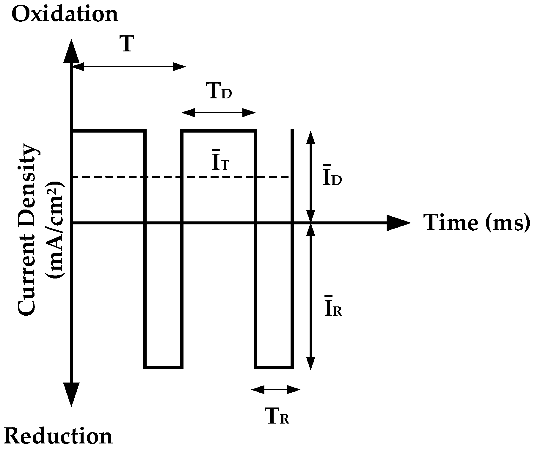
Figure 1. Current density-time diagram applied in pulsed electroplating method. ĪR and ĪD are reverse and direct current density, TR and TD are reverse and direct current application time, ĪT is the average current density, and T is the duration of each periodicity.
Metals 13 00037 g001
Figure 2. Microfabrication process: (A) Sputtering of Cr; (B) Sputtering of Au; (C) KMPR lithography; (D) UV-exposure (patterning); (E) Nickel pulse-reverse electroplating.
Metals 13 00037 g002
Figure 3. Measuring the surface roughness and thickness of the nickel layer using the profilometer.
Metals 13 00037 g003
Figure 4. A sample of evaluating nickel surface roughness and thickness using the profilometer.
Metals 13 00037 g004
Figure 5. Neural network configuration.
Metals 13 00037 g005
Figure 6. Verification of ANN results with experimental results: (a) surface roughness comparison with the experimental result; (b) layer thickness comparison with the experimental result.
Metals 13 00037 g006
Figure 7. The results of the NN prediction on the effect of the beam width at the current density of 20 mA/cm2, stirring speed of 220 rpm, and RTD of 3, relative to (a) thickness of nickel coated layer; (b) surface roughness of nickel coated layer.
Metals 13 00037 g007
Figure 8. The results of the NN prediction on the effect of the stirring speed at the current density of 20 mA/cm2, beam width of 50 μm, and RTD of 3, relative to (a) thickness of nickel coated layer; (b) surface roughness of nickel coated layer.
Metals 13 00037 g008
Figure 9. The results of the NN prediction on the effect of the RTD at the current density of 20 mA/cm2, stirring speed of 220 rpm, and beam width of 50 μm, relative to (a) thickness of nickel coated layer; (b) surface roughness of nickel coated layer.
Metals 13 00037 g009
Figure 10. Optical microscope and SEM images of nickel deposited layer surface with a current density of 20 mA/cm2, stirring speed of 110 rpm, deposition duration of 30 min, and beam width of 50 μm; (a) RTD 2, surface roughness (Ra) = 0.34 μm; (b) RTD 3, surface roughness (Ra) = 0.19 μm; (c) RTD 4, surface roughness (Ra) = 0.08 μm.
Metals 13 00037 g010
Figure 11. The results of the NN prediction on the effect of current density at RTD of 3, beam width of 50 μm, and stirring speed of 220 rpm, relative to (a) thickness of nickel coated layer; (b) surface roughness of nickel coated layer.
Metals 13 00037 g011
Figure 12. 4D diagram of the relationship between current density, RTD, time versus thickness, and surface roughness of nickel at beam width: 50 μm and stirring speed: 180 rpm. (The dashed-dotted lines show the surface roughness value, and the solid lines show the thickness value).
Metals 13 00037 g012
Table 1. Comparison of MSE value of networks with the different number of hidden layer neurons.
The Absolute Mean Value of Training Data Error (%)The Best MSEThe Absolute Mean Value of Test Data Error (%)Number of Neurons
300.07731342-5-5
70.00361302-6-5
0.70.030203.32-7-5
80.02525162-8-5
2.050.00251132-9
4.150.03511202-10-5
Disclaimer/Publisher’s Note: The statements, opinions and data contained in all publications are solely those of the individual author(s) and contributor(s) and not of MDPI and/or the editor(s). MDPI and/or the editor(s) disclaim responsibility for any injury to people or property resulting from any ideas, methods, instructions or products referred to in the content.