Article

Combining 3D Printing and Electrochemical Deposition for Manufacturing Tailor-Made 3D Nickel Foams with Highly Competitive Porosity and Specific Surface Area Density

Center for Electrochemical Surface Technology ZEO, Aalen University of Applied Sciences, Beethovenstr. 1, 73430 Aalen, Germany
*
Author to whom correspondence should be addressed.
Metals 2023, 13(5), 857; https://doi.org/10.3390/met13050857
Submission received: 31 March 2023 / Revised: 17 April 2023 / Accepted: 26 April 2023 / Published: 28 April 2023

Abstract

:
One of the most promising and heavily researched energy storage systems due to their high energy density, rate capability and extended cycle life are lithium-ion batteries. Their performance and efficiency are nonetheless strongly dependent on their constituent materials and design, including the current collectors. One attractive approach in this respect is the use of metal foams as an alternative to the conventional current collectors. This concept is therefore intended to increase the current collectors’ specific surface area and therefore load more active material by nominal area while keeping the cell architectures simple and less costly. In the present work, nickel is chosen as a model system for a proof of concept of a novel manufacturing method for nickel foams using a combination of 3D printing, coating and electroplating. The purpose is to create geometrically well-defined hollow structures with high porosity and specific surface area density that can rival and partially outperform the commercially available nickel foams. To this end, a 3D printer is used to create geometrically flexible and well-defined open-pored disks of HIPS (high-impact polystyrene), which are then spray coated with a graphite-based conducting layer and subsequently electroplated with a 5–30 µm thin layer of nickel from an additive-free nickel sulfamate electrolyte. Following the coating process, the support structure is dissolved with toluene, resulting in structures with a unique combination of porosity in the range of 92.3–99.1% and an ultra-high specific surface area density up to 46 m2/kg. Morphological characterization by light and scanning electron microscopy has proven that the temporarily required polymer substrate can be mildly and completely removed by the suggested room temperature dissolution process.

1. Introduction

Lithium-ion batteries are considered one of the most promising options for energy storage systems due to their long cycle life, high energy density performance and rate capability [1,2,3]. Within a lithium-ion cell, the current collectors play a vital role in facilitating the charge transfer between the active electrode materials and the external circuit [4,5]. Typically, aluminum foil is used as the current collector for the cathode and copper foil for the anode [6]. In this context, research has been conducted to replace conventional 2D foil current collectors for lithium-ion batteries by 3D foams, mainly made out of nickel, but in the future, also out of aluminum [7,8,9]. This is a promising alternative with the potential to improve a variety of performance parameters, safety and assembly costs. Given the high porosity and specific surface area, the hollow volume of the current collector can effectively be filled with active material. Due to the enormous increase in real vs. nominal surface, current densities are lowered. On the other hand, short diffusion paths and high electrolyte accessibility are achieved [10,11,12]. As a result, the main types of overpotentials, namely, the charge transfer and diffusion overpotential, can be reduced [13]. Additionally, foam current collectors can better withstand the mechanical stress and volume changes that occur during battery cycling, leading to improved durability and a longer lifespan [14,15,16]. As already reported, of the two examples of current collector foams, nickel foams remain the most preferred due to their high specific surface area and ability to be fabricated with high porosity. The use of aluminum foams, on the other hand, is still less established, but can offer advantages such as improved conductivity and reduced weight. However, currently, few aluminum foams are available with competitive porosities. Overall, the choice of current collector material and design of the structure [17] is a critical factor in the performance of lithium-ion batteries.
Various sintering processes are applied to produce open-cell foams with a porosity of up to 80% [18]. To produce highly porous open-cell foams (>90%), polymer foams are generally used as templates or substrates. These can be utilized, for example, as molds for a casting process, although the demolding of the solidified metal foam is nonetheless difficult [19]. Furthermore, the polymer foam can serve as a substrate and later coated by CVD [20,21] or electrochemical deposition [22,23] and subsequently pyrolyzed and oxidized. In another process, hydrogen, which is formed as a by-product of electrodeposition from protic solvents, is used as a template for the simultaneously growing metal layer [24]. The latter mainly applies to aqueous electrolytes. In order to produce state-of-the-art, open-cell, highly porous nickel foams, a commonly used substrate is a polyurethane (PU) foam. This is first coated with a conductive layer and subsequently electroplated with nickel [25]. Following the electroplating process, the electroplated PU foam is heated up to 800 °C to remove the PU carrier structure and to retain the highly porous nickel foam. This causes an oxide layer to form on the nickel, which is reduced by the exposure to a hydrogen gas atmosphere at 1000 °C [26]. One of the leading suppliers of nickel foams is Recemat BV, a company that specializes in producing high-quality nickel foams with desirable properties such as high porosity and surface area. The most important parameters for the Recemat Ni-5763 foam, which are the average porosity of 96%, the average specific surface of 6900 m2/m3 and the average specific surface area density of 16.1 m2/kg [27], are commonly used as reference values in research and development work involving nickel foams.
In the current study, a novel method is developed to produce open-pore, highly porous metal foams. For the proof of concept and for direct comparison with the state of the art, nickel is chosen. It is noteworthy that the research focus of the study is on the fabrication of aluminum foams, which will subsequently be reported.
Other publications have already shown that 3D-printed substrates can be electroplated [28,29] or that additive manufacturing can be used to manufacture metal foams [30,31]. In the present work, however, the process of electroplating 3D-printed substrates involves the use of a non-conductive filament. Before the electroplating can occur, the substrate is spray coated with a conducting graphite layer to prepare the substrate surface for electroplating. Once the coating process is complete, the former 3D-printed substrate is dissolved in an organic solvent at room temperature, leaving a hollow 3D metal structure with high porosity, specific surface and specific surface area density.
The proposed method within the present work offers an advantage over the nickel foams currently available on the market. Such foams are produced by electroplating onto randomly structured polymer foams, which are subsequently removed at high temperatures by oxidation and pyrolysis. Our method provides a more straightforward and precise approach, allowing for greater control over the geometry of the hollow structures. By achieving superior porosity and specific surface area density, the structures produced by this method have the potential to compete with the commercially available nickel foams. More importantly, following this initial proof of concept, the latter can be transferred to aluminum, for which the classical state-of-the-art process proves to be critical due to the high oxygen affinity of aluminum.

2. Materials and Methods

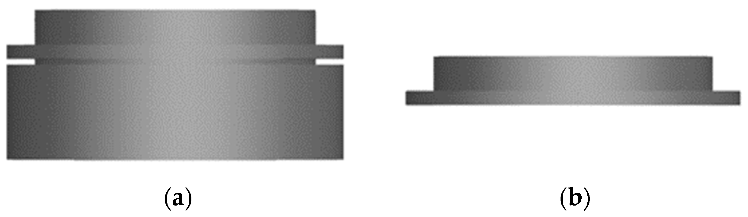
2.1. Modeling and Manufacturing of the Substrates

To create an open porous structure of the substrates, a simple FDM (fused deposition modeling)-based 3D printer (Anycubiy Mega X, ANYCUBIC TECHNOLOGY CO., Hong Kong, China) with a high-impact polystyrene (HIPS) filament (HIPS Extrafill Natura, Fillamentum Manufacturing Czech s.r.o., Hulin, Czech Republic) is used. To prevent any potential warping, the printing plate is carefully fixed with adhesive tape (4124, tesa SE, Norderstedt, Germany) prior to the printing process. The CAD software (NX 12.0, Siemens Digital Industries Software, Plano, TX, USA) is used to design a hollow cylinder with a diameter of 12 mm, a height of 4 mm, a wall thickness of 0.6 mm and an indentation of 0.2 mm depth located 0.5 mm below the top edge. A second hollow cylinder measuring 10 mm diameter, 1.3 mm height and 0.4 mm wall thickness is created on top (Figure 1). The 3D-printed circular blanks are then cut at the notch with a scalpel. Afterwards, the upper part is used as a substrate for the electrochemical deposition and the bottom part is discarded to remove any printing defects that commonly appear in that area.
The size and shape of the substrate are specifically chosen to fit into a coin cell as a current collector.
Two different architectures are generated for the circular substrates, namely, an open and a linked structure. The open structure of the substrate is created by combining four levels, each containing five round struts with a diameter of 0.45 mm. The levels are overlaid and rotated by 60° to form the final structure.
On the other hand, the linked structure consists of eight levels, with each level comprising five round struts with a diameter of 0.45 mm. The strut edges of each new level are situated at the center of the previous level and rotated by 30° to build the final architecture (Figure 2).
The inner surface of the hollow cylinder and the lateral surface of the substrate struts are extracted from CAD software. Notably, the top, bottom and outer bounding surfaces, as well as the complete lower part that is removed after printing, are excluded. The surface areas A determined for the open and linked structures are 289 mm2 and 431 mm2, respectively.

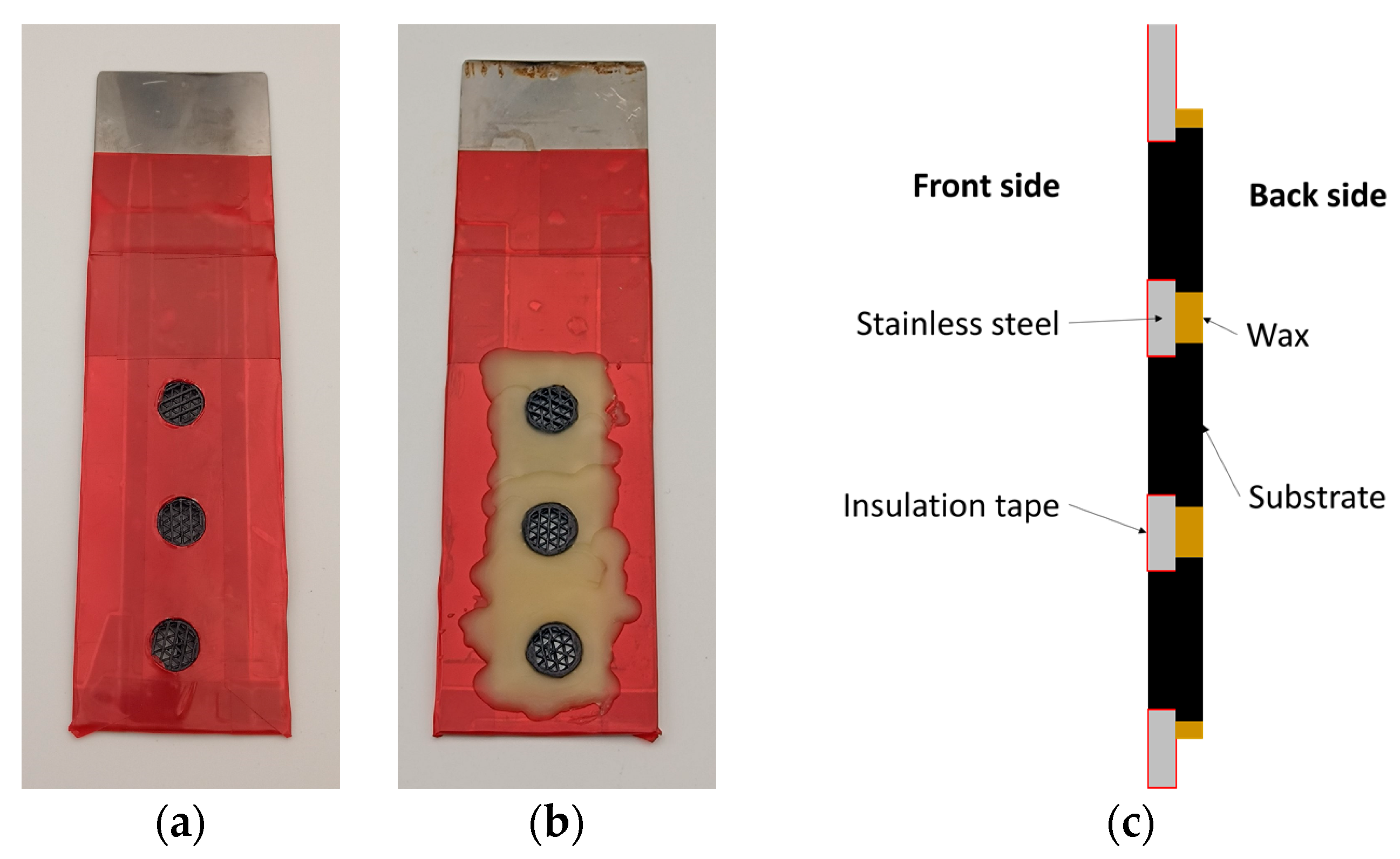
2.2. Substrate Preparation

In order to increase the electrical conductivity of the substrate’s surface, it is spray coated with a lacquer-based graphite suspension (Graphite 33, Kontakt Chemie, Zele, Belgium). A stainless-steel sheet measuring 4 cm × 15 cm with three 10 mm diameter central holes serves as a holder for the subsequent electrodeposition. Thus, three substrates are simultaneously coated in each plating step. The entire surface of the holder is masked with insulating adhesive tape (4154, tesa SE, Norderstedt, Germany) and the holes are then cut free with a scalpel. The substrates are inserted through the holes such that the top of the larger cylinder rests on the bare side of the holder, ensuring the electrical contact. The remaining bare area of the holder is then covered with hot liquid wax, as shown in Figure 3.
Once the wax hardens by cooling at room temperature, the holder is then placed in an ultrasonic degreaser (SLOTOCLEAN AK 340, Dr.-Ing. Max Schlötter GmbH & Co. KG, Geislingen a. d. Steige, Germany) for 1 min at 50 °C, rinsed with deionized water and then activated in a 1:3 HCl acid solution for 30 s. Afterwards, the holder is rinsed once more with deionized water.

2.3. Electrochemical Deposition

An additive-free nickel sulfamate Ni(NH2SO3)2 electrolyte with a pH of 4 ± 0.2 is used for the electrochemical deposition. The electrolyte composition consists of a nickel sulfamate solution (Umicore AG & Co. KG, Hanau, Germany), boric acid B(OH)3 (DIN 50970, WOCKLUM, Balve, Germany) and nickel chloride hexahydrate NiCl2·6H2O (DIN 50970, WOCKLUM, Balve, Germany) with the concentrations given in Table 1.
Throughout the deposition process, the electrolyte’s working temperature is maintained at 50 °C and circulated by the use of a 60 mm stirring bar at 350 rpm to ensure good electrolyte exchange in the substrates. The holder containing the substrates is positioned centrally between two 2.5 cm × 20 cm sulfur depolarized nickel anodes in a 3 L beaker in a way that each substrate’s front and back sides are aligned parallel to the two anodes. A current density of 0.7 A/dm2 is applied, targeting film thicknesses of 28, 10 and 5 µm.

2.4. Three-Dimensionally Printed HIPS Substrate Dissolution

Once coated, the substrates are dipped in toluene (technical grade, Stierand GmbH, Waldstetten, Germany) for a minimum of 12 h, followed by a fresh toluene rinse and a sonication in toluene for 30 min to remove any remaining residues of the carrier structure from the ridges. The substrates are then cleaned with acetone (technical grade, Stierand GmbH, Waldstetten, Germany) and allowed to dry in the air.

2.5. Calculation Basis of Nickel Foam Key Figures

To assess the amount of deposited nickel, the samples are initially weighed after graphite coating using an analytical balance (AUW220D, Shimadzu Deutschland GmbH, Duisburg, Germany). The second step involves weighing the samples again after electrochemical deposition. The difference between the initial weight and the weight after deposition provides a measure of the amount of nickel deposited on the samples. The latter is then used to calculate the average coating thickness d according to Equation (1):
d = m N i A × ρ N i
where d is the average layer thickness, mNi is the nickel mass, A is the substrate area (see Section 2.1) and ρNi is the nickel density.
Additionally, the porosity ε, the specific surface SV and the specific surface density Sm can be determined according to Equations (2)–(4):
ε = V h o l l o w V t o t a l
S V = A s t r u c t u r e V t o t a l
S m = A s t r u c t u r e m N i
where ε is the porosity, Vhollow is the hollow space volume inside the circumscribing cylinder, Vhotal is the total volume of the circumscribing cylinder, SV is the specific surface, Astructure is the surface of the generated structure (inner and outer surface of the struts) and Sm is the specific surface area density.
The total volume is assumed to be a circumscribing cylinder with a diameter of 10 mm and a height of 1.3 mm and the lower outer rim is neglected. To determine the hollow volume of the samples, the deposited nickel volume is divided by the density of the nickel (8.91 g/cm3). The calculated nickel volume is then subtracted from the total volume of the circumscribing cylinder. It is noteworthy that the surface area of the nickel structure doubles compared to the 3D-printed structure, since the filler structure is dissolved after nickel deposition. However, the surface change caused by the increase in the nickel layer is not considered in the calculation as it is neglectable.
The quality of the coating is assessed by a digital light microscope (VHX-6000, KEYENCE DEUTSCHLAND GmbH, Neu-Isenburg, Germany) at various magnifications. A ring light is used for the exposure during the measurements.
A Gemini LEO 1525 (Zeiss, Oberkochen, Germany) scanning electron microscope (SEM) is used to evaluate the morphology of the samples. The microscope is equipped with an energy-dispersive X-ray detector (EDX) to perform elemental mapping. The EDX analysis is operated at an acceleration voltage of 10 kV and allows for the identification and quantification of the chemical elements present in the samples.

3. Results and Discussion

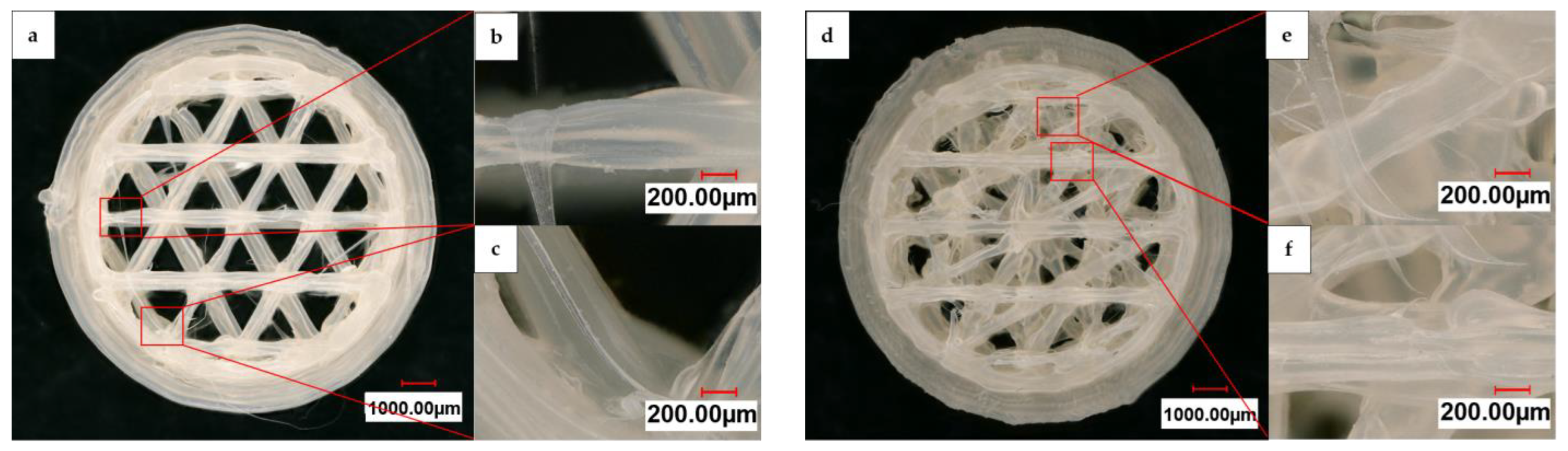
3.1. Characterization of the Printed Substrates by Digital Light Microscopy

Figure 4 displays a digital light microscope panorama image at 200× magnification of a 3D-printed HIPS substrate with an open and linked structure, in addition to individual images of the struts and printing errors. The sample images were taken in the intermediate state prior to the graphite spray coating. The basic structure of the CAD-generated shape was reproduced. However, some slight deviations from the original design can be observed. During printing, the structure struts underwent deformation, resulting in a strut width of 260 µm to 459 µm. Moreover, the 3D-printing process produced artifacts that remained on the substrate structure. Compared to the open structure, the linked one shows more of these artifacts in the form of strings between the struts.

3.2. Characterization of the Nickel Foams by Digital Light Microscopy after Electrochemical Deposition and Dissolution of the 3D-Printed HIPS Substrate

Figure 5 displays a digital light microscope panorama image at 200× magnification from the top and bottom of one nickel foam with an open and one with a linked structure after electrochemical deposition and dissolution of the 3D-printed HIPS substrate. The uniform layer growth on both sides of the nickel foams is visible. However, some flaws resulting from the 3D-printing process are still noticeable even after the metal deposition and dissolution of the substrate. In addition, the outer ring of the lower cylinder appears black when viewed from above as it is lacking a nickel layer, yet has a silvery shine when viewed from below, where it is plated. This is due to the fact that the upper part serves as a contact area to the holder and does not undergo nickel overgrowth, whereas the lower part is not masked and becomes plated. Further partial masking of the inner parts of the substrate was caused by the liquid wax used for coverage, which partially spread over, mainly affecting the outer perimeter. This then prevented the nickel from coating the covered areas and caused detachment. Therefore, like in Figure 5d, the interior of the substrate can also be seen as a black area from the underside of the linked structure.
In the case of the 5 µm deposition on the open structure, it is worth noting that the nickel struts can break off during the ultrasound-assisted dissolution of the 3D-printed HIPS substrate, indicating the insufficient stability of the deposited nickel layer. As shown by the cross sections in Figure 6, in comparison to a Recemat 5763 reference foam, the samples with an open and linked structure after dissolution of the polymer substrate demonstrated an outer silvery nickel layer that grew uniformly deep into the structure in all three transverse sections. The black coloration inside the strut is a result of the conductive coating’s graphite particles present in that area. Likewise, there were no PU residues left inside the commercial nickel foam from Recemat, which was subject to high temperature oxidation and pyrolysis during the manufacturing process, as well as from the 3D-printed HIPS support structure in both of our samples, which was completely dissolved by the low temperature dissolution process. The strut width of the commercial foam (Figure 6b) was approximately one order of magnitude smaller than that of our manufactured samples, while the thicknesses of the hollow struts’ walls were comparable. It is also evident that our samples were open on the cylindrical outer surface, allowing, due to their larger diameter, easier access to the inner surface of the struts.

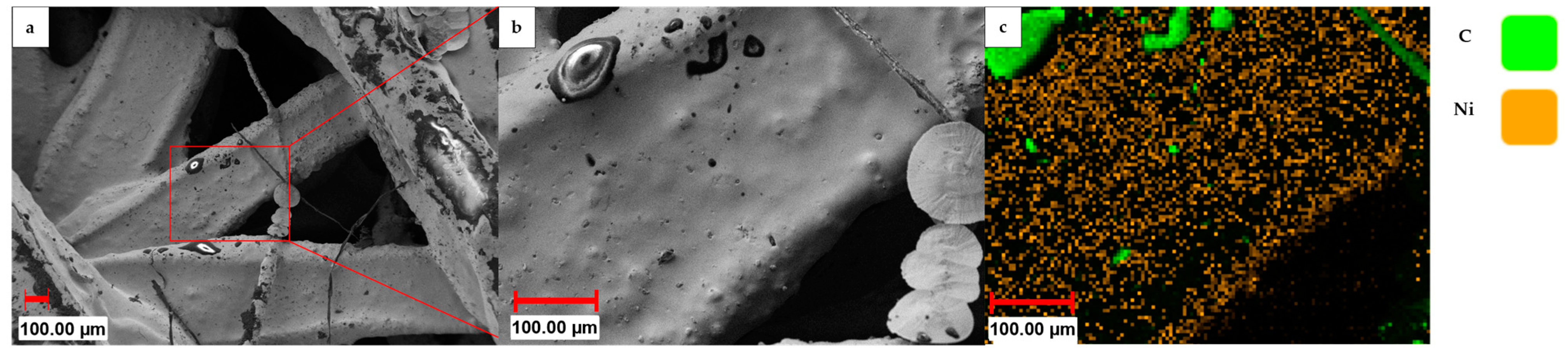
3.3. SEM and EDX Analyses

Displayed in Figure 7 are the results of SEM and EDX analyses of an electroplated linked sample prior to the dissolution of the support structure. The SEM image reveals the presence of thin artifacts in the form of filament threads that are only partially coated, in addition to black spots on the struts, which correspond to carbon, as confirmed by the EDX analysis. This observation indicates that the nickel layer has not entirely plated the whole substrate, probably due to imperfections in the formerly applied graphite layer. This results in a porous nickel layer after the dissolution of the HIPS substrate. Therefore, increasing the current density—which increases the nucleation rate during deposition, especially important for the initial plating phase—can improve the pore-free coverage and plating uniformity of the substrate [32,33].

3.4. Gravimetrically Derived Nickel Layer Thicknesses

Table 2 shows the gravimetrically determined amount of nickel and the calculated average nickel layer thickness of the samples produced by the electrodeposition on substrates with an open fill structure. For this purpose, the individual substrates were weighed after the graphite and nickel coating. To determine the current efficiency, the total amount of nickel electrodeposited in each deposition process (with three individual substrates) was summed up and normalized to the theoretical amount of electrodeposited nickel based on Faraday’s law, assuming a virtual current efficiency of 100%.
The average nickel layer thicknesses are 25.2, 9.0 and 4.5 µm, for targeted average nickel layer thicknesses based on Faraday’s law of 28, 10 and 5 µm. This reveals a real current efficiency of 89.9 ± 0.5%, which is reasonable, as hydrogen evolution is a well-known side reaction in nickel plating. The maximum film thickness deviation of the individual samples per deposition is 3.1, 0.7 and 5.3 µm, respectively, each occurring on the center-positioned sample. The deviation of the determined layer thicknesses between the two outer samples is 0.3, 0.1 and 1.9 µm. During electrochemical deposition, the amount of nickel deposited is lowest on the center-positioned sample. This can be attributed to the electrical field distribution, as the primary current density is naturally higher at the edges and decreases towards the center [32,33]. For future perspectives, by using appropriate additives in combination with an adjusted electrolyte composition, the macro-scattering ability of the electrolyte can be increased and the layer thickness distribution within one and between different samples can be improved.
It is noticeable that in the 5 µm deposition, there is a very high variation in the amount of nickel deposited between the substrates. This is attributed to contact problems of the middle substrate, since the current efficiency of this deposition is comparable to the others. Thus, when the centered substrate is not contacted, more nickel is deposited on the outer substrates.
Table 3 shows the gravimetric-determined amount of nickel and the calculated average thickness of the samples produced by the electrodeposition on substrates with a linked structure. The values are determined in the same way as those with an open structure.
Due to the increased surface area of the linked structure, more nickel has to be deposited (factor 1.5) into the sample to achieve the same layer thickness as the open structure. The average layer thicknesses per deposition are 25.5, 9.4 and 5.0 µm and only deviate by a maximum of 0.5 µm from the deposition on the open structure. Therefore, an average current efficiency of 95 ± 4% is achieved. Here, too, it can be observed that the center-positioned sample always has the lowest nickel layer thickness. The maximum nickel layer thickness deviations of the individual samples per deposition are 2.3, 1.0 and 1.8 µm. Likewise, the respective deviation of the layer thicknesses of the two outer samples is small (1.3, 0.3 and 0.6 µm).

3.5. Determination of the Nickel Foam Key Figures

Table 4 and Table 5 show the porosity, specific surface and specific surface area density of the samples with open and linked structures.
Both structures show that the porosity of the samples increases as expected with decreasing nickel layer thickness. The open structure reaches a maximum of 99.1 ± 0.4% and the linked structure a maximum of 98.5 ± 0.2%. The specific surface is independent of the layer thickness, but solely depends on the chosen geometry. For the open and linked structures, the specific surface values are 4087 and 6091 m2/m3, respectively. The specific surface area density increase is indirectly proportional to the nickel layer thickness. This is perfectly reproducible for targeted nickel layer thicknesses of 28 and 10 µm and should, for a nickel layer thickness of 5 µm, finally reach approximately 50 m2/kg for the open and 48 m2/kg for the linked samples. Due to a greater variance in the electroplating results, which is partially due to incomplete nickel coverage, the obtained results for a Ni layer thickness of 5 µm deviate. While for the linked substrate, the value of 46.2 ± 7.3 m2/kg is plausible, the value of 71.6 ± 46.7 m2/kg for the open substrate suggests that the obtained nickel coverage is only about 70%, on average. As a conclusion, nickel layer thicknesses in the range of only 5 µm seem to be at the lower limit of reproducible conditions or may already be beyond this limit, depending on the chosen geometry.

4. Conclusions and Outlook

In the present work, a new and versatile way of manufacturing highly competitive metal foams is suggested and investigated on the basis of nickel. One of the advantages of additive manufacturing is the geometrical freedom of these substrates and their high reproducibility. In this way, the structure and key parameters can be adjusted in a wide range and adopted very well to the respective target application, e.g., as a battery current collector. In this case, the specific surface could be further enhanced, or a vertically open structure could be created to improve slurry infiltration.
By varying the deposited nickel layer thickness, the porosity and specific surface area density can be adjusted, partially outperforming the parameters of commercially available nickel foams. However, a nickel layer thickness of less than 5 µm is not applicable, as this significantly reduces the homogeneity, integrity and mechanical stability of the obtained nickel foams.
It is shown that the 3D-printed HIPS substrates can be completely removed after nickel deposition using toluene as a solvent, thereby eliminating the need for a high temperature oxidation and pyrolysis process. The latter may negatively impact the metal layer in general, especially if the process should be transferred to more susceptible metals such as aluminum, which is planned to be subject of our future investigation.
Therefore, the aim of this work was to first show that the described alternative process in general, even when using a low-budget 3D printer, can compete and partially outperform classical metal foam manufacturing processes. This can be accomplished while achieving important target parameters such as porosity, specific surface and specific surface area density, at the same time allowing the adjustment and optimization of the structure for the individual target application.
Secondly, we hereby provide a new strategy for the manufacturing of highly competitive metal foams, where the electrodeposition method in the long term will allow for the use of a wide range of metals, especially aluminum. To assess the benefit of making use of the third dimension, one can also compare the obtained Ni layer thicknesses with those of the state-of-the-art current collector foils used in battery electrode production. These are 10 µm for copper (anode side) and 12 µm for aluminum (cathode side), ensuring sufficient mechanical stability when being handled and coated. Here, with a nickel layer thickness in the range of 9–10 µm, we are comparably competitive. The main advantage therefore results from the high enlargement factor from the nominal to real surface, which is 7.4 for the open and 11.0 for the linked structure. This, at the battery cell level, would result in significant mass savings of electrolytes and separators, as they would only need to correspond to the nominal surface.

Author Contributions

Conceptualization, T.S.; methodology, T.S.; software, R.A., O.K. and W.E.M.; validation, R.A. and O.K.; formal analysis, R.A., O.K. and W.E.M.; investigation, R.A., O.K. and W.E.M.; resources, T.S.; data curation, R.A. and O.K.; writing—original draft preparation, R.A. and W.E.M.; writing—review and editing, R.A., T.S. and W.E.M.; visualization, R.A.; supervision, T.S.; project administration, O.K. and T.S.; funding acquisition, T.S. All authors have read and agreed to the published version of the manuscript.

Funding

This research was funded by the German Federal Ministry of Education and Research (BMBF) within the FH-Impuls program under grant number 13FH4I07IA (SmartPro: project Smart-BAT). Funding from the open access publication fund of the Ministry of Science, Research and the Arts MWK of Baden-Württemberg was likewise received.

Data Availability Statement

Not applicable.

Acknowledgments

The support of the Center for Electrochemical Surface Technology ZEO students and members at Aalen University of Applied Sciences is appreciated.

Conflicts of Interest

The authors declare no conflict of interest.

References

  1. Li, M.; Lu, J.; Chen, Z.; Amine, K. 30 years of lithium-ion batteries. Adv. Mater. 2018, 30, 1800561. [Google Scholar] [CrossRef] [PubMed]
  2. Olabi, A.G.; Abbas, Q.; Shinde, P.A.; Abdelkareem, M.A. Rechargeable batteries: Technological advancement, challenges, current and emerging applications. Energy 2023, 266, 126408. [Google Scholar] [CrossRef]
  3. Winter, M.; Barnett, B.; Xu, K. Before Li ion batteries. Chem. Rev. 2018, 118, 11433–11456. [Google Scholar] [CrossRef] [PubMed]
  4. Issatayev, N.; Nuspeissova, A.; Kalimuldina, G.; Bakenov, Z. Three-dimensional foam-type current collectors for rechargeable batteries: A short review. J. Power Sources Adv. 2021, 10, 100065. [Google Scholar] [CrossRef]
  5. Rahman, A.; Rahman, M.; Song, G. A review on binder-free NiO-Ni foam as anode of high performance lithium-ion batteries. Energy Storage 2021, 4, e278. [Google Scholar] [CrossRef]
  6. Theivaprakasam, S.; Girard, G.; Howlett, P.; Forsyth, M.; Mitra, S.; MacFarlane, D. Passivation behaviour of aluminium current collector in ionic liquid alkyl carbonate (hybrid) electrolytes. NPJ Mater. Degrad. 2018, 2, 13. [Google Scholar] [CrossRef]
  7. Jin, S.; Jiang, Y.; Ji, H.; Yu, Y. Advanced 3d current collectors for lithium-based batteries. Adv. Mater. 2018, 30, e1802014. [Google Scholar] [CrossRef]
  8. Yamada, M.; Watanabe, T.; Gunji, T.; Wu, J.; Matsumoto, F. Review of the Design of Current Collectors for Improving the Battery Performance in Lithium-Ion and Post-Lithium-Ion Batteries. Electrochem 2020, 1, 11. [Google Scholar] [CrossRef]
  9. Jiang, W.W.; Li, J.J.; Ye, C.Z.; Zhang, J.; Huang, L.; Wu, X.; Hu, Z.M.; Li, W.J.; Dai, Y.; Sun, F.G. Lightweight 3D porous Al foams for the hosts of high-performance Li metal anodes. CCS Chem. 2023, 39, 291–299. [Google Scholar]
  10. Yang, G.F.; Song, K.Y.; Joo, S.K. A metal foam as a current collector for high power and high capacity lithium iron phosphate batteries. J. Mater. Chem. A 2014, 2, 19648–19652. [Google Scholar] [CrossRef]
  11. Wang, J.S.; Liu, P.; Sherman, E.; Verbrugge, M.; Tataria, H. Formulation and characterization of ultra-thick electrodes for high energy lithium-ion batteries employing tailored metal foams. J. Power Sources 2011, 196, 8714–8718. [Google Scholar] [CrossRef]
  12. Fritsch, M.; Standke, G.; Heubner, C.; Langklotz, U.; Michaelis, A. 3D-cathode design with foam-like aluminum current collector for high energy density lithium-ion batteries. J. Energy Storage 2018, 16, 125–132. [Google Scholar] [CrossRef]
  13. Huang, G.; Chen, S.; Guo, P.; Tao, R.; Jie, K.; Liu, B.; Zhang, X.; Liang, J.; Cao, Y.-C. In situ constructing lithiophilic NiFx nanosheets on Ni foam current collector for stable lithium metal anode via a succinct fluorination strategy. Chem. Eng. J. 2020, 395, 125122. [Google Scholar] [CrossRef]
  14. Yao, M.; Okuno, K.; Iwaki, T.; Awazu, T.; Sakai, T. Long cycle-life LiFePO4/Cu-Sn lithium ion battery using foam-type three-dimensional current collector. J. Power Sources 2010, 195, 2077–2081. [Google Scholar] [CrossRef]
  15. Bastawros, A. Experimental analysis of deformation mechanisms in a closed-cell aluminum alloy foam. J. Mech. Phys. Solids 2000, 48, 301–322. [Google Scholar] [CrossRef]
  16. Badiche, X.; Forest, S.; Guibert, T.; Bienvenu, Y.; Bartout, J.-D.; Ienny, P.; Croset, M.; Bernet, H. Mechanical properties and non-homogeneous deformation of open-cell nickel foams: Application of the mechanics of cellular solids and of porous materials. Mater. Sci. Eng. A 2000, 289, 276–288. [Google Scholar] [CrossRef]
  17. Jung, A.; Diebels, S. Micromechanical Characterization of Metal Foams. Adv. Eng. Mater. 2019, 21, 1900237. [Google Scholar] [CrossRef]
  18. Atwater, M.; Guevara, L.; Darling, K.; Tschopp, M. Solid State Porous Metal Production: A Review of the Capabilities, Characteristics, and Challenges. Adv. Eng. Mater. 2018, 20, 1700766. [Google Scholar] [CrossRef]
  19. Banhart, J. Manufacture, characterisation and application of cellular metals and metal foams. Prog. Mater. Sci. 2001, 46, 559–632. [Google Scholar] [CrossRef]
  20. Queheillalt, D.; Hass, D.; Sypeck, D.; Wadley, H. Synthesis of open-cell metal foams by templated directed vapor deposition. J. Mater. Res. 2001, 16, 1028–1036. [Google Scholar] [CrossRef]
  21. Paserin, V.; Marcuson, S.; Wilkinson, J. CVD Technique for Inco Nickel Foam Production. Adv. Eng. Mater. 2004, 6, 454–459. [Google Scholar] [CrossRef]
  22. Brown, I.; Sotiropoulos, S. Electroplating and electroless plating of Ni through/onto a porous polymer in a flow cell. J. Appl. Electrochem. 2001, 31, 1203–1212. [Google Scholar] [CrossRef]
  23. Sundarram, S.; Jiang, W.; Li, W. Fabrication of Small Pore-Size Nickel Foams Using Electroless Plating of Solid-State Foamed Immiscible Polymer Blends. J. Manuf. Sci. Eng. 2014, 136, 021002. [Google Scholar] [CrossRef]
  24. Cherevko, S.; Xing, X.; Chung, C. Electrodepostion of three-dimensional porousl silver foams. Electrochem. Commun. 2010, 12, 467–470. [Google Scholar] [CrossRef]
  25. Onck, P.R.; van Merkerk, R.; Raaijmakers, A.; de Hosson, J.T.M. Fracture of open- and closed-cell metal foams. J. Mater. Sci. 2005, 40, 5821–5828. [Google Scholar] [CrossRef]
  26. Recemat, B.V. About Recemat Metalfoam. Available online: https://www.recemat.nl/metalfoam/ (accessed on 30 March 2023).
  27. Recemat, B.V. Data Sheet Nickelfoam. Available online: https://www.recemat.nl/wp-content/uploads/2020/08/Datasheet_Ni.pdf (accessed on 30 March 2023).
  28. Hüner, B.; Demir, N.; Kaya, M.F. Lectrodeposition of NiCu bimetal on 3D printed electrodes for hydrogen evolution reactions in alkaline media. Int. J. Hydrogen Energy 2022, 47, 12136–12146. [Google Scholar] [CrossRef]
  29. Kim, M.J.; Cruz, M.A.; Ye, S.; Gray, A.L.; Smith, G.L.; Lazarus, N.; Walker, C.J.; Sigmarsson, H.H.; Wiley, B.J. One-step electrodeposition of copper on conductive 3D printed objects. Addit. Manuf. 2019, 27, 318–326. [Google Scholar] [CrossRef]
  30. Constanza, G.; Del Ferraro, A.; Tata, M. Experimental Set-Up of the Production Process and Mechanical Characterization of Metal Foams Manufactured by Lost-PLA Technique with Different Cell Morphology. Metals 2022, 12, 1385. [Google Scholar] [CrossRef]
  31. Dubinin, O.N.; Bondareva, J.V.; Kuzminova, Y.O.; Simonov, A.P.; Varfolomeev, I.A.; Yakimchuk, I.V.; Evlashin, S.A. A promising approach to 3D printing of metal foam with defined porosity. J. Porous Mater. 2023. [Google Scholar] [CrossRef]
  32. Plieth, W. Electrochemistry for Materials Science; Elsevier Science: Amsterdam, The Netherlands, 2008. [Google Scholar]
  33. Paunovic, M.; Schlesinger, M. Fundamentals of Electrochemical Deposition, 1st ed.; Wiley VHC: Weinheim, Germany, 1998. [Google Scholar]
Figure 1. CAD drawing of the 3D-printed blanks from the side view (a) directly after 3D printing and (b) after removing the bottom part.
Metals 13 00857 g001
Figure 2. CAD drawings of the 3D-printed open substrate (a) from an angled view and (b) from a top view, and of the 3D-printed linked substrate (c) from an angled view and (d) from a top view.
Metals 13 00857 g002aMetals 13 00857 g002b
Figure 3. Pictures of the holder with the substrates after being covered with insulating tape and wax presented from (a) the front side, (b) the back side and (c) their corresponding cross section schematic drawing.
Metals 13 00857 g003
Figure 4. Digital light microscope panorama images at 200× magnification of (a) an open and (d) a linked substrate after printing with individual images of the struts and printing artifacts (b,c,e,f).
Metals 13 00857 g004
Figure 5. Digital light microscope panorama images at 200× magnification from the front and back (a,b) of an open and (c,d) of a linked nickel foam after the dissolution of the carrier structure.
Metals 13 00857 g005
Figure 6. Digital light microscope panorama images at 200× magnification of cross sections of (a) Recemat Ni 5763 foam (d), an open and (g) a linked sample, with individual images at 500× magnification (b,e,h).; (b) shows five cut struts surrounding a circular uncut strut structure to which the cut struts are structurally connected; (e,h) show cut strut structures of the open and linked sample, respectively, and (c,f,i) their corresponding inset zoom images.
Metals 13 00857 g006
Figure 7. (a,b) SEM images and (c) elemental mapping of an electroplated linked sample prior to the dissolution of the 3D-printed HIPS substrate.
Metals 13 00857 g007
Table 1. Composition and concentrations of the nickel sulfamate electrolyte.
ChemicalsConcentration (g/L)
Ni concentration from Ni(NH2SO3)2110
NiCl2·6 H2O3.3
B(OH)330
Table 2. Results of the gravimetrically derived nickel layer thicknesses for the open samples.
Targeted Average Nickel Layer Thickness Based on Faraday’s Law with a Virtual Current Efficiency of 100%
(µm)
Position of the Substrate on the HolderMass of Nickel
Deposited (mg)
Calculated Average Nickel Layer Thickness Based on the Given Substrate’s Geometry (µm)
28Top67.726.3
Center59.723.2
Bottom67.026.0
10Top24.19.3
Center22.18.6
Bottom23.79.2
5Top12.85
Center4.21.6
Bottom17.76.9
Table 3. Results of the gravimetrically derived nickel layer thicknesses for the linked samples.
Targeted Average Nickel Layer Thickness Based on Faraday’s Law with a Virtual Current Efficiency of 100%
(µm)
Position of the Substrate on the HolderMass of Nickel
Deposited (mg)
Calculated Average Nickel Layer Thickness Based on the Given Substrate’s Geometry (µm)
28Top102.626.7
Center93.524.4
Bottom97.525.4
10Top37.59.8
Center33.98.8
Bottom36.49.5
5Top19.95.2
Center15.34.0
Bottom22.15.8
Table 4. Key figures of the open structure nickel foams.
Targeted Average Nickel Layer Thickness Based on Faraday’s Law with a Virtual Current Efficiency of 100%
(µm)
Porosity
(%)
Specific Surface
(m2/m3)
Specific Surface Area Density (m2/kg)
2894.9 ± 0.340878.9 ± 0.5
1098.2 ± 0.124.9 ± 0.9
599.1 ± 0.471.6 ± 46.7
Table 5. Key figures of the linked structure nickel foams.
Targeted Average Nickel Layer Thickness Based on Faraday’s Law with a Virtual Current Efficiency of 100%
(µm)
Porosity
(%)
Specific Surface
(m2/m3)
Specific Surface Area Density (m2/kg)
2892.3 ± 1.460918.8 ± 0.3
1097.2 ± 0.124.0 ± 1.0
598.5 ± 0.246.2 ± 7.3
Disclaimer/Publisher’s Note: The statements, opinions and data contained in all publications are solely those of the individual author(s) and contributor(s) and not of MDPI and/or the editor(s). MDPI and/or the editor(s) disclaim responsibility for any injury to people or property resulting from any ideas, methods, instructions or products referred to in the content.

