Simulation of Mechanical and Thermal Loads and Microtexturing of Ceramic Cutting Inserts in Turning a Nickel-Based Alloy


 ,
, 
Abstract
:1. Introduction
- increased formation of brittle structures in the near-surface layer (the formation of second-order secondary compounds on the heating surface, due to the material’s active oxidation as a result of the interaction of the molten material of the cutting insert/substrate and coating with the environment) [30];
- (TiCrAlSi)N coating was used as a basis;
- The basic layer consisted of (CrTi)N and (AlTi)N layers that alternated;
- An (AlTiCr)N/SiN nanocomposite layer was on top of this;
- The nanocomposite layer was formed as an amorphous Si3N4 with evenly distributed (AlTiCr)N crystals 5 nm in size.
- linear microtextures with a continuously rewinding tool electrode (wire electrical discharge machining); each groove may be identical to the previous one due to the constant updating of the tool electrode in the processing area [35];
- regular microtextures made using electrical discharge die sinking with a prefabricated electrode [36];
- regular microtextures made using electrical discharge drilling with a universal hollow wire electrode [37].
- Wire electrical discharge machining, taking into account the spark gap and wire diameter of 0.25 mm;
- Electrical discharge drilling, taking into account the minimum possible diameter of the tool electrode.
2. Materials and Methods
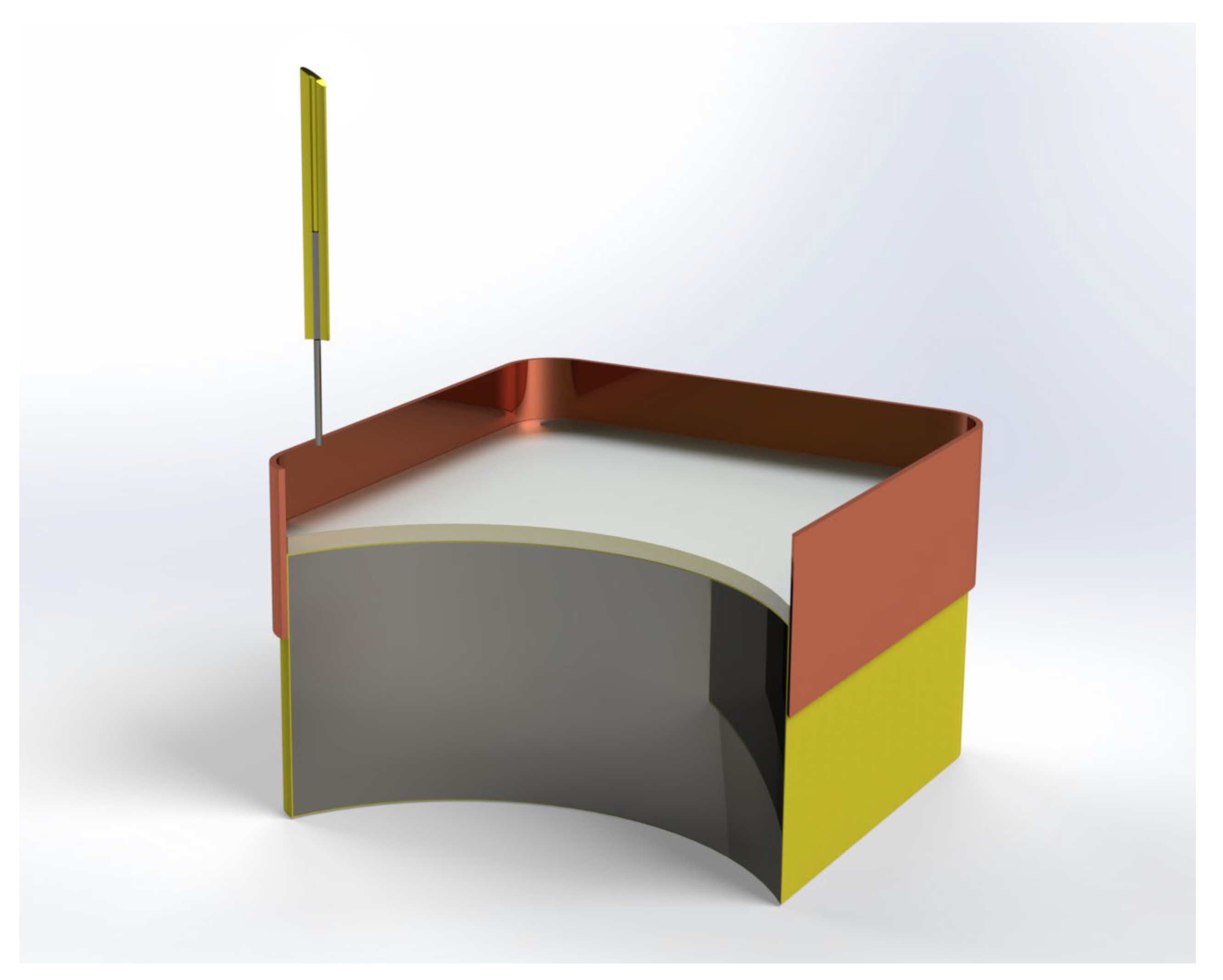
2.1. Ceramic Cutting Inserts and Microtextures
- SNGN150716T02520 6190, Sandvik Coromant (Sandviken, Sweden) (a square-shaped indexable insert for turning cast iron and hard alloy).
2.2. Modeling of Mechanical and Thermal Loads
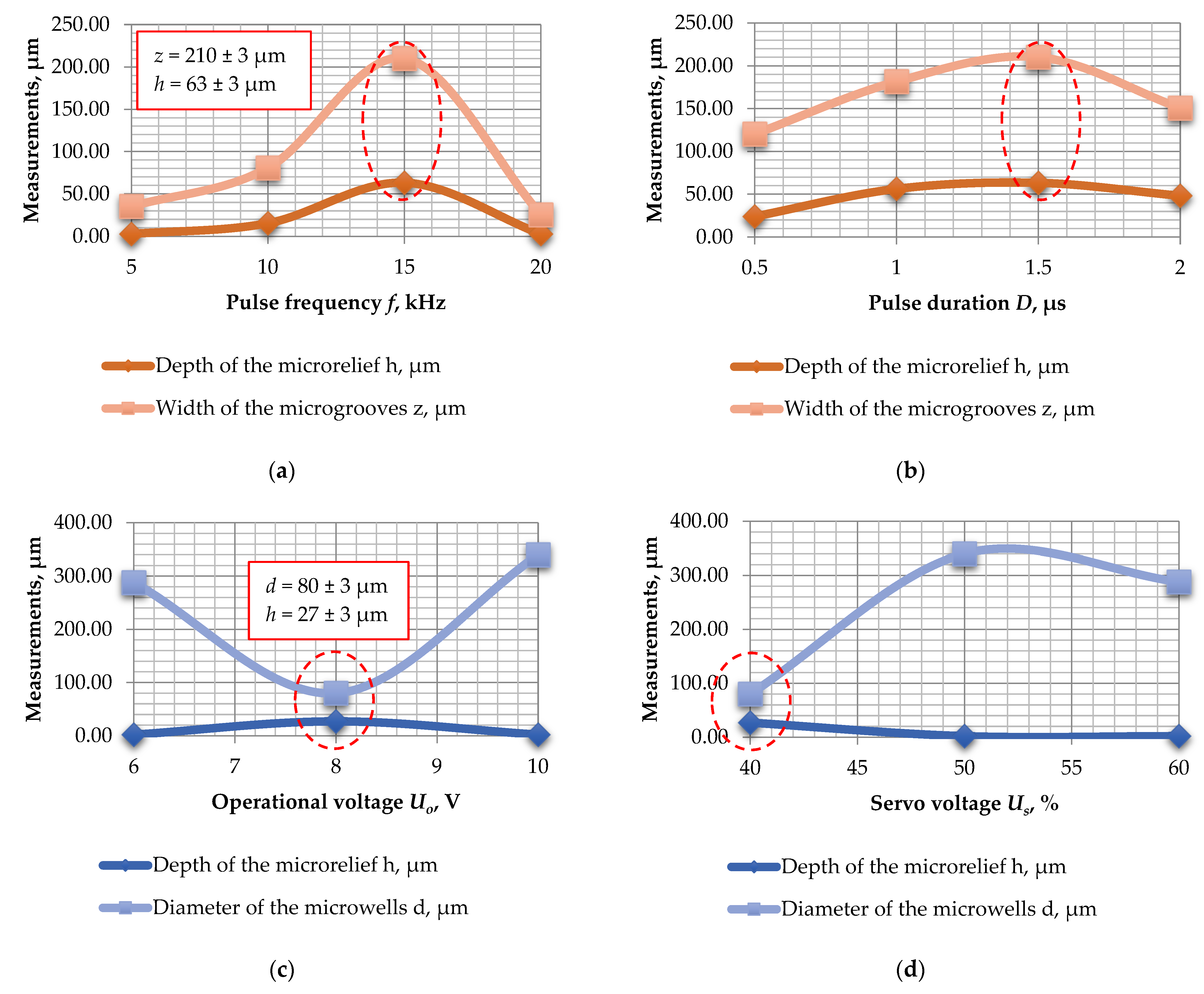
2.3. Microtexturing using Electrical Discharge Machining
2.4. Assisting Powder-Mixed Medium
2.5. Multifunctional Coating
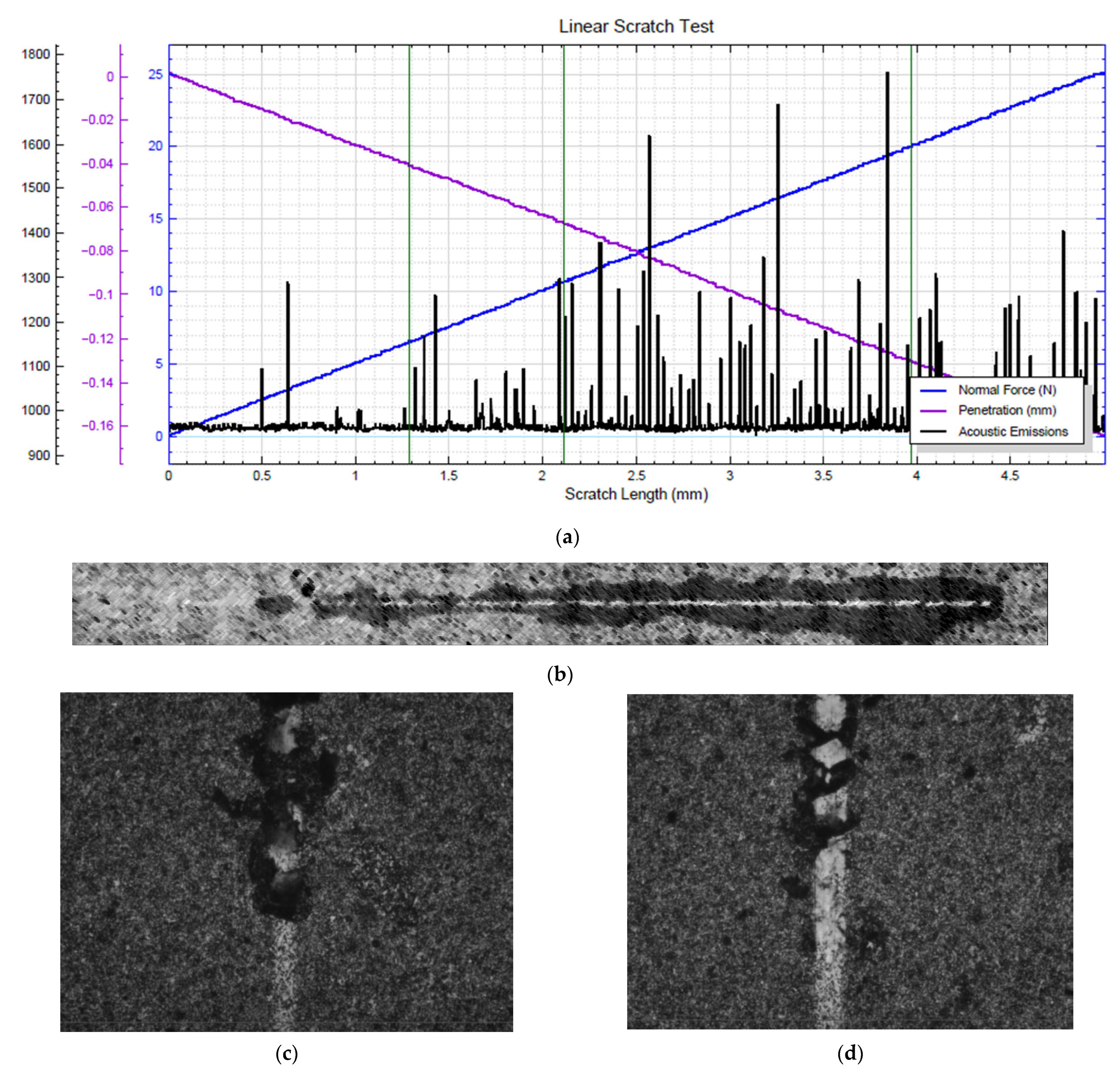
2.6. Resistance Tests
3. Results
3.1. Modeling and Development of the Microtextures
- 2–3 microgrooves at an inclination of 45° to the axis of symmetry of the cutting edge on the insert’s rake face (designed for production via wire electrical discharge machining with a universal brass/tungsten wire electrode with a diameter of 0.125–0.1 mm);
- 6–9 evenly distributed microwells/holes symmetrically located to the axis of symmetry of the cutting edge on the insert’s rake face (designed for production using an electrical discharge super drill with a universal brass/tungsten wire ø0.1 mm in diameter);
- 2–3 wavy grooves with a radius of R300 µm at an inclination of 45° to the axis of symmetry of the cutting edge on the insert’s rake face (designed for production via electrical discharge die sinking with a complex profile electrode made of M2 copper, a second-order tool);
- 3 × 3 lattice microtexture with a step of 200 µm at an inclination of 45° to the axis of symmetry of the cutting edge on the insert’s rake face (designed for production via electrical discharge die sinking with a complex profile electrode made of M2 copper, a second-order tool).
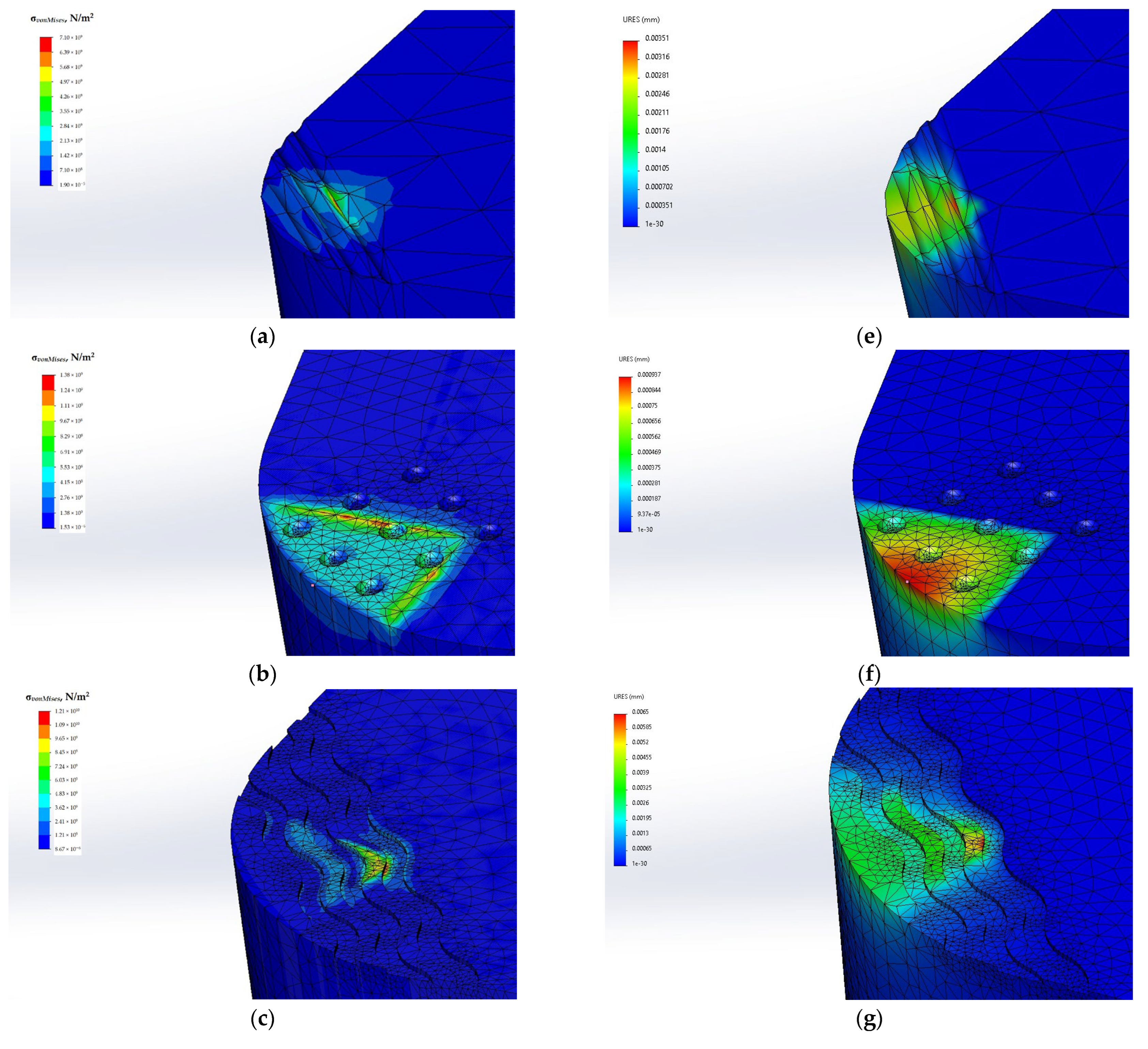
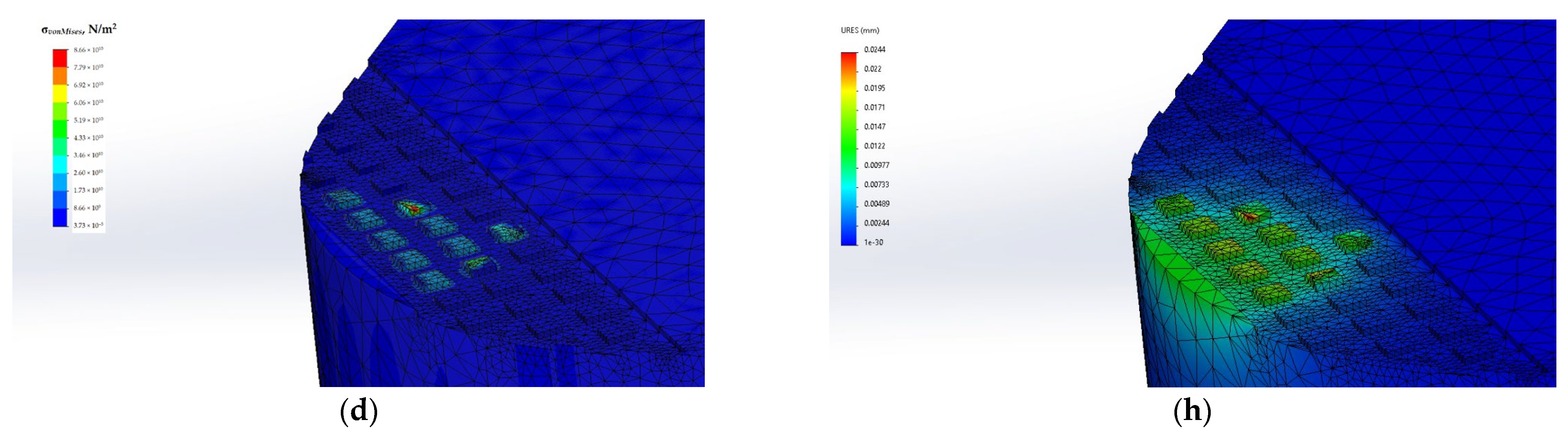
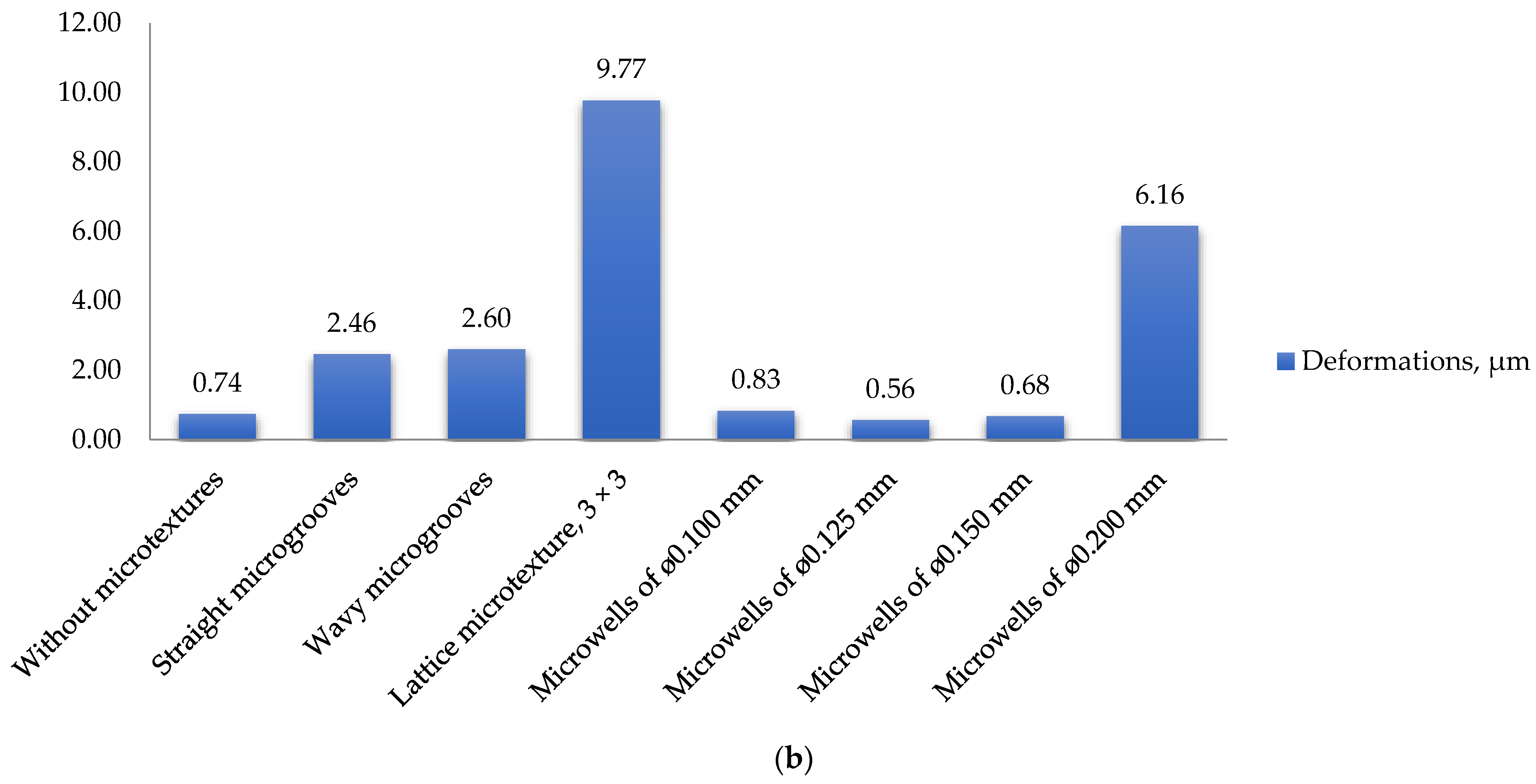
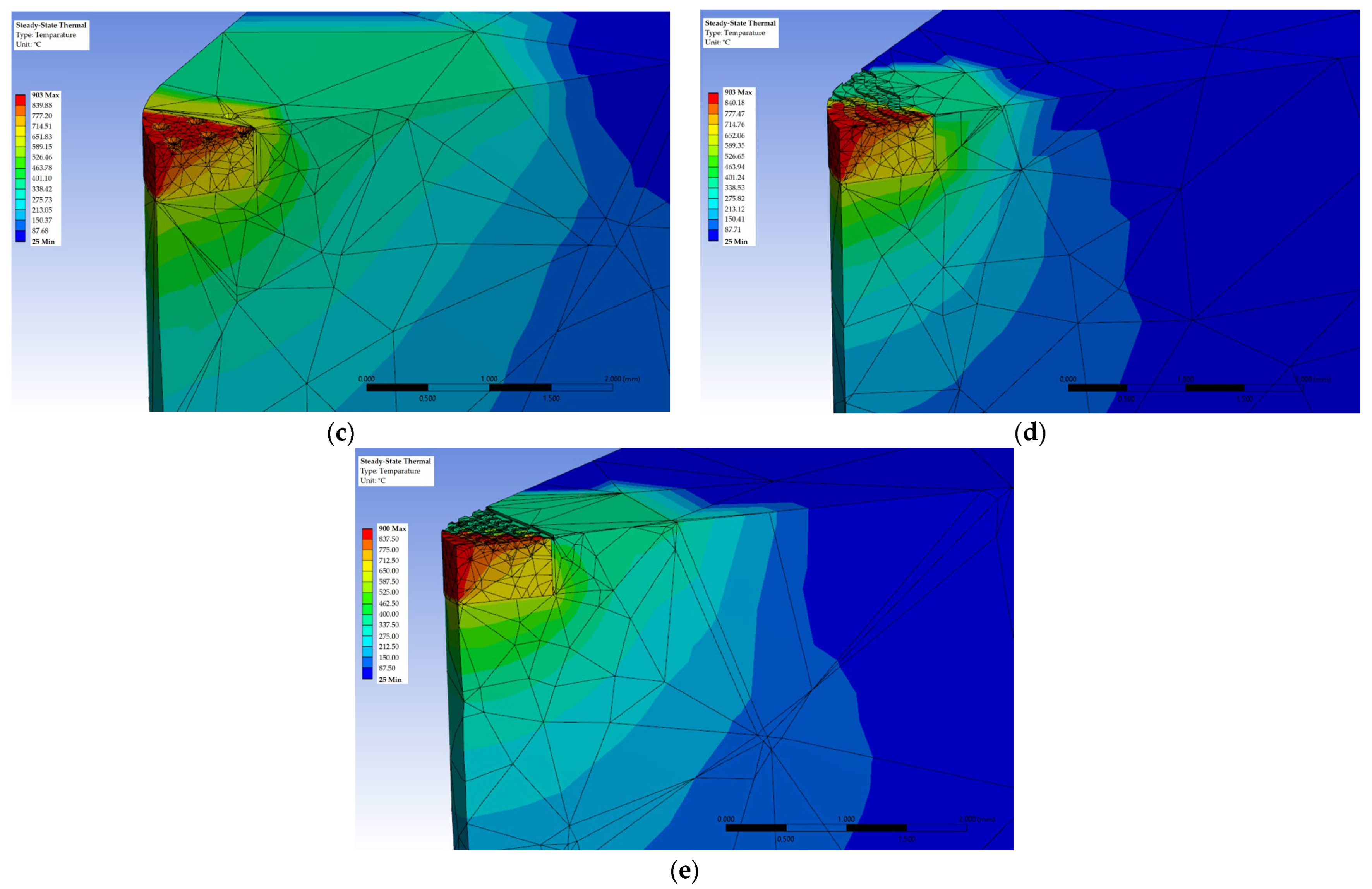
3.2. Simulation of Mechanical and Thermal Loads
- -
- an insert without microtextures;
- -
- an insert with three straight microgrooves at an inclination of 45°;
- -
- an insert with a set of nine microwells/holes of ø0.125 mm in diameter;
- -
- an insert with three wavy microgrooves at an inclination of 45°;
- -
- an insert with a 3 × 3 lattice microtexture.
- -
- an insert without microtextures;
- -
- an insert with three straight microgrooves at an inclination of 45°;
- -
- an insert with a set of nine microwells/holes of ø0.125 mm in diameter;
- -
- an insert with three wavy microgrooves at an inclination of 45°;
- -
- an insert with a 3 × 3 lattice microtexture.
3.3. Properties of Deposited Multifunctonal Coatings
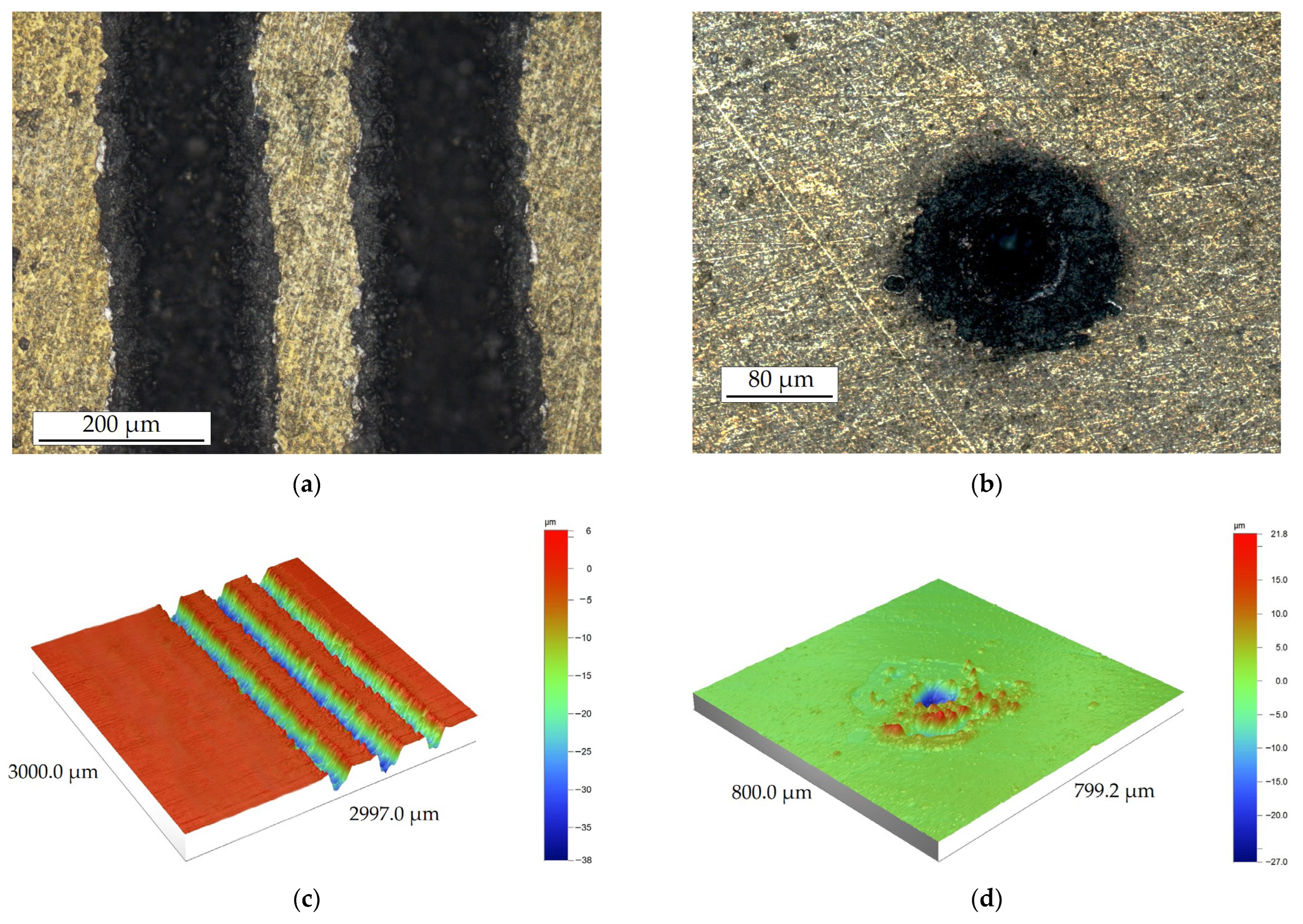
3.4. Characterization of Microtextures
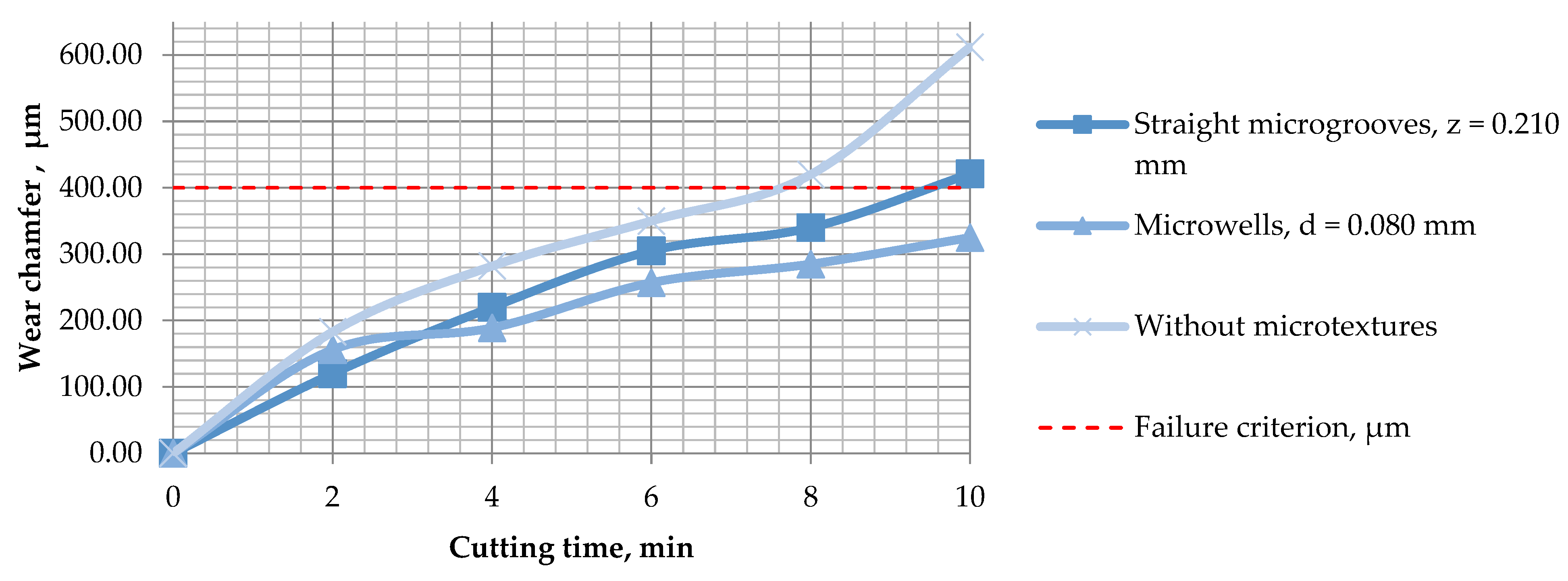
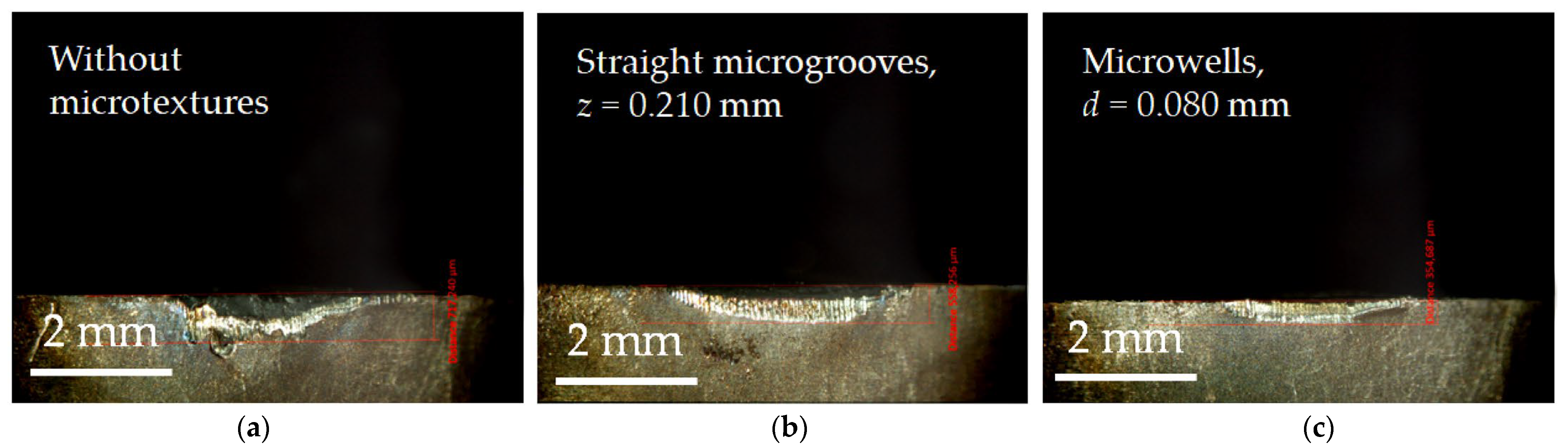
3.5. Wear Resistance of Microtextured Cutting Inserts
4. Conclusions
- developing the various shaped microtextures;
- the adaptation of the developed microtextures according to the chosen technology of production (innovative assistance electrode electrical discharge machining in a TiO2 powder mixed suspension);
- simulation of the mechanical (Px = −89.475 N, Py = −81.225 N, Pz = −39.915 N) and thermal loads (Tmax = 900 °C) in the contact pad.
Author Contributions
Funding
Data Availability Statement
Acknowledgments
Conflicts of Interest
References
- Grigoriev, S.; Volosova, M.; Mosyanov, M.; Fedorov, S. The Study of Radius End Mills with TiB2 Coating When Milling a Nickel Alloy. Materials 2023, 16, 2535. [Google Scholar] [CrossRef]
- Asiltürk, İ.; Kuntoğlu, M.; Binali, R.; Akkuş, H.; Salur, E. A Comprehensive Analysis of Surface Roughness, Vibration, and Acoustic Emissions Based on Machine Learning during Hard Turning of AISI 4140 Steel. Metals 2023, 13, 437. [Google Scholar] [CrossRef]
- Migranov, M.S.; Shehtman, S.R.; Sukhova, N.A.; Mitrofanov, A.P.; Gusev, A.S.; Migranov, A.M.; Repin, D.S. Study of Tribotechnical Properties of Multilayer Nanostructured Coatings and Contact Processes during Milling of Titanium Alloys. Coatings 2023, 13, 171. [Google Scholar] [CrossRef]
- Feng, X.; Fan, X.; Hu, J.; Wei, J. Multi-Objective Optimization Design of Micro-Texture Parameters of Tool for Cutting GH4169 during Spray Cooling. Lubricants 2023, 11, 249. [Google Scholar] [CrossRef]
- Sharma, V.; Pandey, P.M. Recent advances in turning with textured cutting tools: A review. J. Clean. Prod. 2016, 137, 701–715. [Google Scholar] [CrossRef]
- Lei, S.; Devarajan, S.; Chang, Z. A study of micropool lubricated cutting tool in machining of mild steel. J. Mater. Process. Technol. 2009, 209, 1612–1620. [Google Scholar] [CrossRef]
- Sun, J.; Zhou, Y.; Deng, J.; Zhao, J. Effect of hybrid texture combining micro-pits and micro-grooves on cutting performance of WC/Co-based tools. Int. J. Adv. Manuf. Technol. 2016, 86, 3383–3394. [Google Scholar] [CrossRef]
- Feng, X.; Fan, X.; Hu, J.; Wei, J. Research on Cutting Temperature of GH4169 Turning with Micro-Textured Tools. Appl. Sci. 2023, 13, 6832. [Google Scholar] [CrossRef]
- Stebulyanin, M.; Ostrikov, E.; Migranov, M.; Fedorov, S. Improving the Efficiency of Metalworking by the Cutting Tool Rake Surface Texturing and Using the Wear Predictive Evaluation Method on the Case of Turning an Iron–Nickel Alloy. Coatings 2022, 12, 1906. [Google Scholar] [CrossRef]
- Wu, Z.; Deng, J.; Su, C.; Luo, C.; Xia, D. Performance of the micro-texture self-lubricating and pulsating heat pipe self-cooling tools in dry cutting process. Int. J. Refract. Met. Hard Mater. 2014, 45, 238–248. [Google Scholar] [CrossRef]
- Li, K.; Du, J.; Liu, L.; Shen, F.; Ma, L.; Pang, M. Effect of texture parameters on main cutting Force and temperature of cutting tools. Tool Eng. 2019, 53, 42–46. [Google Scholar]
- Deng, J.; Song, W.; Zhang, H.; Yan, P.; Liu, A. Friction and wear behaviors of the carbide tools embedded with solid lubricants in sliding wear tests and in dry cutting processes. Wear 2011, 270, 666–674. [Google Scholar] [CrossRef]
- Deng, J.; Wu, Z.; Lian, Y.; Qi, T.; Cheng, J. Performance of carbide tools with textured rake-face filled with solid lubricants in dry cutting processes. Int. J. Refract. Met. Hard Mater. 2012, 30, 164–172. [Google Scholar]
- Fatima, A.; Whitehead, D.J.; Mativenga, P.T. Femtosecond laser surface structuring of carbide tooling for modifying contact phenomena. Proc. Inst. Mech. Eng. Part B J. Eng. Manuf. 2014, 228, 1325–1337. [Google Scholar] [CrossRef]
- Xing, Y.; Deng, J.; Zhao, J.; Zhang, G.; Zhang, K. Cutting performance and wear mechanism of nanoscale and microscale textured Al2O3/TiC ceramic tools in dry cutting of hardened steel. Int. J. Refract. Met. Hard Mater. 2014, 43, 46–58. [Google Scholar] [CrossRef]
- Fatima, A.; Mativenga, P.T. A comparative study on cutting performance of rake-flank face structured cutting tool in orthogonal cutting of AISI/SAE 4140. Int. J. Adv. Manuf. Technol. 2014, 78, 2097–2106. [Google Scholar] [CrossRef]
- Xing, Y.; Deng, J.; Li, S.; Yue, H.; Meng, R.; Gao, P. Cutting performance and wear characteristics of Al2O3/TiC ceramic cutting tools with WS2/Zr soft-coatings and nano-textures in dry cutting. Wear 2014, 318, 12–26. [Google Scholar] [CrossRef]
- Grigoriev, S.N.; Volosova, M.A.; Okunkova, A.A. Investigation of Surface Layer Condition of SiAlON Ceramic Inserts and Its Influence on Tool Durability When Turning Nickel-Based Superalloy. Technologies 2023, 11, 11. [Google Scholar] [CrossRef]
- Padhan, S.; Das, S.R.; Das, A.; Alsoufi, M.S.; Ibrahim, A.M.M.; Elsheikh, A. Machinability Investigation of Nitronic 60 Steel Turning Using SiAlON Ceramic Tools under Different Cooling/Lubrication Conditions. Materials 2022, 15, 2368. [Google Scholar] [CrossRef] [PubMed]
- Gevorkyan, E.; Rucki, M.; Panchenko, S.; Sofronov, D.; Chałko, L.; Mazur, T. Effect of SiC Addition to Al2O3 Ceramics Used in Cutting Tools. Materials 2020, 13, 5195. [Google Scholar] [CrossRef] [PubMed]
- Grigoriev, S.N.; Volosova, M.A.; Peretyagin, P.Y.; Seleznev, A.E.; Okunkova, A.A.; Smirnov, A. The Effect of TiC Additive on Mechanical and Electrical Properties of Al2O3 Ceramic. Appl. Sci. 2018, 8, 2385. [Google Scholar] [CrossRef] [Green Version]
- Khmyrov, R.S.; Grigoriev, S.N.; Okunkova, A.A.; Gusarov, A.V. On the possibility of selective laser melting of quartz glass. Phys. Procedia 2014, 56, 345–356. [Google Scholar] [CrossRef] [Green Version]
- Khmyrov, R.S.; Protasov, C.E.; Grigoriev, S.N.; Gusarov, A.V. Crack-free selective laser melting of silica glass: Single beads and monolayers on the substrate of the same material. Int. J. Adv. Manuf. Technol. 2016, 85, 1461–1469. [Google Scholar] [CrossRef]
- Gavrilov, G.; Kurkin, A.; Rusin, E.; Bazhenov, E. Laser Drilling in Alumina Ceramics Using a Combination of Laser Pulses in the Free-Running and Q-Switched Modes. Materials 2023, 16, 3457. [Google Scholar] [CrossRef] [PubMed]
- Yadroitsev, I.; Bertrand, P.; Antonenkova, G.; Grigoriev, S.; Smurov, I. Use of track/layer morphology to develop functional parts by selectivelaser melting. J. Laser Appl. 2013, 25, 052003. [Google Scholar] [CrossRef]
- Gusarov, A.V.; Grigoriev, S.N.; Volosova, M.A.; Melnik, Y.A.; Laskin, A.; Kotoban, D.V.; Okunkova, A.A. On productivity of laser additive manufacturing. J. Mater. Process. Technol. 2018, 261, 213–232. [Google Scholar] [CrossRef]
- Metel, A.S.; Stebulyanin, M.M.; Fedorov, S.V.; Okunkova, A.A. Power Density Distribution for Laser Additive Manufacturing (SLM): Potential, Fundamentals and Advanced Applications. Technologies 2019, 7, 5. [Google Scholar] [CrossRef] [Green Version]
- Murzin, S.P. Laser Irradiation for Enhancing Mass Transfer in the Solid Phase of Metallic Materials. Metals 2021, 11, 1359. [Google Scholar] [CrossRef]
- Metel, A.S.; Grigoriev, S.N.; Tarasova, T.V.; Filatova, A.A.; Sundukov, S.K.; Volosova, M.A.; Okunkova, A.A.; Melnik, Y.A.; Podrabinnik, P.A. Influence of Postprocessing on Wear Resistance of Aerospace Steel Parts Produced by Laser Powder Bed Fusion. Technologies 2020, 8, 73. [Google Scholar] [CrossRef]
- Okunkova, A.A.; Shekhtman, S.R.; Metel, A.S.; Suhova, N.A.; Fedorov, S.V.; Volosova, M.A.; Grigoriev, S.N. On Defect Minimization Caused by Oxide Phase Formation in Laser Powder Bed Fusion. Metals 2022, 12, 760. [Google Scholar] [CrossRef]
- Smurov, I.; Doubenskaia, M.; Grigoriev, S.; Nazarov, A. Optical Monitoring in Laser Cladding of Ti6Al4V. J. Therm. Spray Tech. 2012, 21, 1357–1362. [Google Scholar] [CrossRef]
- Doubenskaia, M.; Pavlov, M.; Grigoriev, S.; Tikhonova, E.; Smurov, I. Comprehensive Optical Monitoring of Selective Laser Melting. J. Laser Micro Nanoeng. 2012, 7, 236–243. [Google Scholar]
- Metel, A.S.; Grigoriev, S.N.; Tarasova, T.V.; Melnik, Y.A.; Volosova, M.A.; Okunkova, A.A.; Podrabinnik, P.A.; Mustafaev, E.S. Surface Quality of Metal Parts Produced by Laser Powder Bed Fusion: Ion Polishing in Gas-Discharge Plasma Proposal. Technologies 2021, 9, 27. [Google Scholar] [CrossRef]
- Grigoriev, S.N.; Nadykto, A.B.; Volosova, M.A.; Zelensky, A.A.; Pivkin, P.M. WEDM as a Replacement for Grinding in Machining Ceramic Al2O3-TiC Cutting Inserts. Metals 2021, 11, 882. [Google Scholar] [CrossRef]
- Chen, Y.; Hu, S.; Li, A.; Cao, Y.; Zhao, Y.; Ming, W. Parameters Optimization of Electrical Discharge Machining Process Using Swarm Intelligence: A Review. Metals 2023, 13, 839. [Google Scholar] [CrossRef]
- Ablyaz, T.R.; Shlykov, E.S.; Muratov, K.R.; Osinnikov, I.V.; Bannikov, M.V.; Sidhu, S.S. Investigation of Plasma-Electrolytic Processing on EDMed Austenitic Steels. Materials 2023, 16, 4127. [Google Scholar] [CrossRef]
- Machno, M.; Matras, A.; Szkoda, M. Modelling and Analysis of the Effect of EDM-Drilling Parameters on the Machining Performance of Inconel 718 Using the RSM and ANNs Methods. Materials 2022, 15, 1152. [Google Scholar] [CrossRef]
- Grigoriev, S.N.; Okunkova, A.A.; Volosova, M.A.; Hamdy, K.; Metel, A.S. Electrical Discharge Machining of Al2O3 Using Copper Tape and TiO2 Powder-Mixed Water Medium. Technologies 2022, 10, 116. [Google Scholar] [CrossRef]
- Okunkova, A.A.; Volosova, M.A.; Hamdy, K.; Gkhashim, K.I. Electrical Discharge Machining of Alumina Using Cu-Ag and Cu Mono- and Multi-Layer Coatings and ZnO Powder-Mixed Water Medium. Technologies 2023, 11, 6. [Google Scholar] [CrossRef]
- Fukuzawa, Y.; Tani, T.; Mohri, N. Machining characteristics of insulated Si3N4 ceramics by electrical discharge method—Use of powder-mixed machining fluid. J. Ceram. Soc. Jpn. 2000, 108, 184–190. [Google Scholar] [CrossRef] [Green Version]
- Volosova, M.A.; Okunkova, A.A.; Fedorov, S.V.; Hamdy, K.; Mikhailova, M.A. Electrical Discharge Machining Non-Conductive Ceramics: Combination of Materials. Technologies 2020, 8, 32. [Google Scholar] [CrossRef]
- Volosova, M.; Okunkova, A.; Peretyagin, P.; Melnik, Y.A.; Kapustina, N. On Electrical Discharge Machining of Non-Conductive Ceramics: A Review. Technologies 2019, 7, 55. [Google Scholar] [CrossRef] [Green Version]
- Lukashenko, S.V.; Kovtun, A.V.; Dashuk, P.N.; Sokolov, B.N. The Method of Electrical Discharge Machining of Dielectrics. Patent 1,542,715, 10 December 1986. [Google Scholar]
- Liu, Y.H.; Li, X.P.; Ji, R.J.; Yu, L.L.; Zhang, H.F.; Li, Q.Y. Effect of technological parameter on the process performance for electric discharge milling of insulating Al₂O₃ ceramic. J. Mater. Process. Technol. 2008, 208, 245–250. [Google Scholar] [CrossRef]
- Guo, Y.; Hou, P.; Shao, D.; Li, Z.; Wang, L.; Tang, L. High-Speed Wire Electrical Discharge Machining of Insulating Zirconia with a Novel Assisting Electrode. Mater. Manuf. Process. 2014, 29, 526–531. [Google Scholar] [CrossRef]
- Kumar, A.; Mandal, A.; Dixit, A.R.; Das, A.K. Performance evaluation of Al₂O₃ nano powder mixed dielectric for electric discharge machining of Inconel 825. Mater. Manuf. Process. 2018, 33, 986–995. [Google Scholar] [CrossRef]
- Tzeng, Y.F.; Lee, C.Y. Effects of powder characteristics on electrodischarge machining efficiency. Int. J. Adv. Manuf. Technol. 2001, 17, 586–592. [Google Scholar] [CrossRef]
- Zhang, W.; Li, L.; Wang, N.; Teng, Y.L. Machining of 7Cr13Mo steel by US-PMEDM process. Mater. Manuf. Process. 2021, 9, 1060–1066. [Google Scholar] [CrossRef]
- Grigoriev, S.N.; Gurin, V.D.; Volosova, M.A.; Cherkasova, N.Y. Development of residual cutting tool life prediction algorithm by processing on CNC machine tool. Mater. Werkst. 2013, 44, 790–796. [Google Scholar] [CrossRef]
- Grigoriev, S.N.; Kozochkin, M.P.; Sabirov, F.S.; Kutin, A.A. Diagnostic systems as basis for technological improvement. Proc. CIRP 2012, 1, 599–604. [Google Scholar] [CrossRef] [Green Version]
- Grigoriev, S.N.; Sinopalnikov, V.A.; Tereshin, M.V.; Gurin, V.D. Control of parameters of the cutting process on the basis of diagnostics of the machine tool and workpiece. Meas. Tech. 2012, 55, 555–558. [Google Scholar] [CrossRef]
- Grigoriev, S.N.; Volosova, M.A.; Okunkova, A.A.; Fedorov, S.V.; Hamdy, K.; Podrabinnik, P.A.; Pivkin, P.M.; Kozochkin, M.P.; Porvatov, A.N. Electrical Discharge Machining of Oxide Nanocomposite: Nanomodification of Surface and Subsurface Layers. J. Manuf. Mater. Process. 2020, 4, 96. [Google Scholar] [CrossRef]
- Okunkova, A.A.; Volosova, M.A.; Kropotkina, E.Y.; Hamdy, K.; Grigoriev, S.N. Electrical Discharge Machining of Alumina Using Ni-Cr Coating and SnO Powder-Mixed Dielectric Medium. Metals 2022, 12, 1749. [Google Scholar] [CrossRef]
- Hou, P.; Guo, Y.; Shao, D.; Li, Z.; Wureli, Y.; Tang, L. Influence of open-circuit voltage on high-speed wire electrical discharge machining of insulating Zirconia. Int. J. Adv. Manuf. Technol. 2014, 73, 229–239. [Google Scholar] [CrossRef]
- Moudood, M.A.; Sabur, A.; Ali, M.Y.; Jaafar, I.H. Effect of Peak Current on Material Removal Rate for Electrical Discharge Machining of Non-Conductive Al2O3 Ceramic. Adv. Mater. Res. 2014, 845, 730–734. [Google Scholar] [CrossRef]
- Grigoriev, S.N.; Volosova, M.A.; Okunkova, A.A.; Fedorov, S.V.; Hamdy, K.; Podrabinnik, P.A. Elemental and Thermochemical Analyses of Materials after Electrical Discharge Machining in Water: Focus on Ni and Zn. Materials 2021, 14, 3189. [Google Scholar] [CrossRef] [PubMed]
- Rashid, A.; Bilal, A.; Liu, C.; Jahan, M.P.; Talamona, D.; Perveen, A. Effect of Conductive Coatings on Micro-Electro-Discharge Machinability of Aluminum Nitride Ceramic Using On-Machine-Fabricated Microelectrodes. Materials 2019, 12, 3316. [Google Scholar] [CrossRef] [PubMed] [Green Version]
- Tsui, H.-P.; Hsu, S.-Y. Study on Fe-Based Metallic Glass Micro Hole Machining by Using Micro-EDM Combined with Electrophoretic Deposition Polishing. Processes 2022, 10, 96. [Google Scholar] [CrossRef]
- Grigoriev, S.N.; Teleshevskii, V.I. Measurement Problems in Technological Shaping Processes. Meas. Tech. 2011, 54, 744–749. [Google Scholar] [CrossRef]
- Zakharov, O.V.; Brzhozovskii, B.M. Accuracy of centering during measurement by roundness gauges. Meas. Tech. 2006, 49, 1094–1097. [Google Scholar] [CrossRef]
- Rezchikov, A.F.; Kochetkov, A.V.; Zakharov, O.V. Mathematical models for estimating the degree of influence of major factors on performance and accuracy of coordinate measuring machines. MATEC Web Conf. 2017, 129, 01054. [Google Scholar] [CrossRef] [Green Version]
- Zakharov, O.V.; Balaev, A.F.; Kochetkov, A.V. Modeling Optimal Path of Touch Sensor of Coordinate Measuring Machine Based on Traveling Salesman Problem Solution. Procedia Eng. 2017, 206, 1458–1463. [Google Scholar] [CrossRef]
- Low, I.-M. An Overview of Parameters Controlling the Decomposition and Degradation of Ti-Based Mn+1AXn Phases. Materials 2019, 12, 473. [Google Scholar] [CrossRef] [PubMed] [Green Version]
- Pyachin, S.A.; Burkov, A.A.; Makarevich, K.S.; Zaitsev, A.V.; Karpovich, N.F.; Ermakov, M.A. Optical characteristics of particles produced using electroerosion dispersion of titanium in hydrogen peroxide. Tech. Phys. 2016, 61, 1046–1052. [Google Scholar] [CrossRef]
- Sahu, A.K.; Chatterjee, S.; Nayak, P.K.; Mahapatra, S.S. Study on effect of tool electrodes on surface finish during electrical discharge machining of Nitinol. IOP Conf. Ser. Mate. Sci. Eng. 2018, 338, 012033. [Google Scholar] [CrossRef] [Green Version]
- Movchan, B.A.; Grechanyuk, N.I. Microhardness and microbrittleness of condensates of the TiC-Al2O3 system. Inorg. Mater. 1981, 17, 972–973. [Google Scholar]
- Calka, A.; Wexler, D. Mechanical milling assisted by electrical discharge. Nature 2002, 419, 147–151. [Google Scholar] [CrossRef] [PubMed]
- Grigoriev, S.N.; Volosova, M.A.; Okunkova, A.A.; Fedorov, S.V.; Hamdy, K.; Podrabinnik, P.A.; Pivkin, P.M.; Kozochkin, M.P.; Porvatov, A.N. Wire Tool Electrode Behavior and Wear under Discharge Pulses. Technologies 2020, 8, 49. [Google Scholar] [CrossRef]
- Grigoriev, S.N.; Kozochkin, M.P.; Porvatov, A.N.; Volosova, M.A.; Okunkova, A.A. Electrical discharge machining of ceramic nanocomposites: Sublimation phenomena and adaptive control. Heliyon 2019, 5, e02629. [Google Scholar] [CrossRef] [Green Version]
- Grigoriev, S.N.; Volosova, M.A.; Okunkova, A.A.; Fedorov, S.V.; Hamdy, K.; Podrabinnik, P.A. Sub-Microstructure of Surface and Subsurface Layers after Electrical Discharge Machining Structural Materials in Water. Metals 2021, 11, 1040. [Google Scholar] [CrossRef]
- Grigoriev, S.N.; Metel, A.S.; Tarasova, T.V.; Filatova, A.A.; Sundukov, S.K.; Volosova, M.A.; Okunkova, A.A.; Melnik, Y.A.; Podrabinnik, P.A. Effect of Cavitation Erosion Wear, Vibration Tumbling, and Heat Treatment on Additively Manufactured Surface Quality and Properties. Metals 2020, 10, 1540. [Google Scholar] [CrossRef]
- Prieto-Novoa, G.; Vallejo, F.; Piamba, O.; Olaya, J.; Pineda, Y. Effects of Cr Concentration on the Structure and the Electrical and Optical Properties of Ti-Al-Cr-N Thin Films Prepared by Means of Reactive Co-Sputtering. Crystals 2022, 12, 1831. [Google Scholar] [CrossRef]
- Volosova, M.A.; Grigoriev, S.N.; Kuzin, V.V. Effect of tinaium nitride coatings on stress structural inhomogeneity in oxide-carbide ceramic. Part 2. Concentrated force action. Refract. Ind. Ceram. 2015, 55, 487–491. [Google Scholar] [CrossRef]
- Metel, A.; Bolbukov, V.; Volosova, M.; Grigoriev, S.; Melnik, Y. Equipment for deposition of thin metallic films bombarded by fast argon atoms. Instrum. Exp. Technol. 2014, 57, 345–351. [Google Scholar] [CrossRef]
- Vereschaka, A.A.; Volosova, M.A.; Grigoriev, S.N.; Vereschaka, A.S. Development of wear-resistant complex for high-speed steel tool when using process of combined cathodic vacuum arc deposition. Procedia CIRP 2013, 9, 8–12. [Google Scholar] [CrossRef] [Green Version]
- Metel, A.; Grigoriev, S.; Melnik, Y.; Panin, V.; Prudnikov, V. Cutting Tools Nitriding in Plasma Produced by a Fast Neutral Molecule Beam. Jpn. J. Appl. Phys. 2011, 50, 08JG04. [Google Scholar] [CrossRef]
- Vereschaka, A.; Tabakov, V.; Grigoriev, S.; Sitnikov, N.; Milovich, F.; Andreev, N.; Bublikov, J. Investigation of wear mechanisms for the rake face of a cutting tool with a multilayer composite nanostructured Cr–CrN-(Ti,Cr,Al,Si)N coating in high-speed steel turning. Wear 2019, 438, 203069. [Google Scholar] [CrossRef]
- Vereschaka, A.; Tabakov, V.; Grigoriev, S.; Sitnikov, N.; Milovich, F.; Andreev, N.; Sotova, C.; Kutina, N. Investigation of the influence of the thickness of nanolayers in wear-resistant layers of Ti-TiN-(Ti,Cr,Al)N coating on destruction in the cutting and wear of carbide cutting tools. Surf. Coat. Technol. 2020, 385, 125402. [Google Scholar] [CrossRef]
- Vopát, T.; Sahul, M.; Haršáni, M.; Vortel, O.; Zlámal, T. The Tool Life and Coating-Substrate Adhesion of AlCrSiN-Coated Carbide Cutting Tools Prepared by LARC with Respect to the Edge Preparation and Surface Finishing. Micromachines 2020, 11, 166. [Google Scholar] [CrossRef] [Green Version]
- Bobzin, K.; Brögelmann, T.; Kruppe, N.C.; Carlet, M. Nanocomposite (Ti,Al,Cr,Si)N HPPMS coatings for high performance cutting tools. Surf. Coat. Technol. 2019, 378, 124857. [Google Scholar] [CrossRef]
- Grigoriev, S.N.; Hamdy, K.; Volosova, M.A.; Okunkova, A.A.; Fedorov, S.V. Electrical discharge machining of oxide and nitride ceramics: A review. Mater. Des. 2021, 209, 109965. [Google Scholar] [CrossRef]
- Grigoriev, S.N.; Volosova, M.A.; Fedorov, S.V.; Okunkova, A.A.; Pivkin, P.M.; Peretyagin, P.Y.; Ershov, A. Development of DLC-Coated Solid SiAlON/TiN Ceramic End Mills for Nickel Alloy Machining: Problems and Prospects. Coatings 2021, 11, 532. [Google Scholar] [CrossRef]
- Grigoriev, S.N.; Volosova, M.A.; Vereschaka, A.A.; Sitnikov, N.N.; Milovich, F.; Bublikov, J.I.; Fyodorov, S.V.; Seleznev, A.E. Properties of (Cr,Al,Si)N-(DLC-Si) composite coatings deposited on a cutting ceramic substrate. Ceram. Int. 2020, 46, 18241–18255. [Google Scholar] [CrossRef]
- Grigoriev, S.; Pristinskiy, Y.; Volosova, M.; Fedorov, S.; Okunkova, A.; Peretyagin, P.; Smirnov, A. Wire electrical discharge machining, mechanical and tribological performance of TiN reinforced multiscale SiAlON ceramic composites fabricated by spark plasma sintering. Appl. Sci. 2021, 11, 657. [Google Scholar] [CrossRef]
- Fedorov, S.V.; Pavlov, M.D.; Okunkova, A.A. Effect of structural and phase transformations in alloyed subsurface layer of hard-alloy tools on their wear resistance during cutting of high-temperature alloys. J. Frict. Wear 2013, 34, 190–198. [Google Scholar] [CrossRef]
- Grigoriev, S.N.; Fedorov, S.V.; Pavlov, M.D.; Okunkova, A.A.; So, Y.M. Complex surface modification of carbide tool by Nb plus Hf plus Ti alloying followed by hardfacing (Ti plus Al)N. J. Frict. Wear 2013, 34, 14–18. [Google Scholar] [CrossRef]
- Vereschaka, A.A.; Grigoriev, S.N.; Volosova, M.A.; Batako, A.; Vereschaka, A.S.; Sitnikov, N.N.; Seleznev, A.E. Nano-scale multi-layered coatings for improved efficiency of ceramic cutting tools. Int. J. Adv. Manuf. Technol. 2017, 90, 27–43. [Google Scholar] [CrossRef]
- Grigoriev, S.N.; Vereschaka, A.A.; Fyodorov, S.V.; Sitnikov, N.N.; Batako, A.D. Comparative analysis of cutting properties and nature of wear of carbide cutting tools with multi-layered nano-structured and gradient coatings produced by using of various deposition methods. Int. J. Adv. Manuf. Technol. 2017, 90, 3421–3435. [Google Scholar] [CrossRef]
- ASTM C1624-05; Standard Test Method for Adhesion Strength and Mechanical Failure Modes. ASTM: West Conshohocken, PA, USA, 2010.
- Grigoriev, S.N.; Volosova, M.A.; Fedorov, S.V.; Migranov, M.S.; Mosyanov, M.; Gusev, A.; Okunkova, A.A. The Effectiveness of Diamond-like Carbon a-C:H:Si Coatings in Increasing the Cutting Capability of Radius End Mills When Machining Heat-Resistant Nickel Alloys. Coatings 2022, 12, 206. [Google Scholar] [CrossRef]


| Cutting Tool | Coating | Workpiece | Microtextures | Testing | Performance Effect | Reference |
|---|---|---|---|---|---|---|
| Carbide cutting insert (tungsten carbide, K313) | Uncoated | 1045 steel | Microwells of 70 µm in a diameter by a femtosecond laser | Turning, V = 120 m/min, t = 0.1 mm, s = 0.3 mm/rpm, with lubricant | Reduced the mean cutting forces by 10–30%, and the chip–tool contact length by 30% | [6] |
| Carbide cutting insert (WC/Co-based) | Uncoated | 1045 steel | Grooves/wells of by a femtosecond laser | Turning, with lubricant | Reduced the temperature by 21.7% | [7] |
| Carbide cutting insert (CNMA120408-KR-3225) | TiCN + Al2O3 + TiN composition, CVD | GH4169, Fe/Ni-based superalloy | Grooves/wells of 50 µm in a width/diameter by a femtosecond laser | Turning, V = 50 m/min, t = 0.2 mm, s = 0.2 mm/rpm, with lubricant | Reduced the temperature by 23% | [8] |
| Carbide cutting insert (TK20) | Multi-nanocomposite coating ((CrTi)N/(AlTi)N layers alternation + (AlTiCr)N/SiN nanostructure), PVD | C0.3Cr15Ni35Mo7Mn7Fe, Fe/Ni-based superalloy | 4 lines of microwells of 30 µm in a width by laser and nanoindentation | Turning, V = 17–27 m/min, s = 0.1–0.15 mm/rpm, t = 0.3–0.5 mm, with MoS2-based lubricant | Increased durability by 1.3–1.5 times | [9] |
| Carbide cutting insert (WC/Co-based) | Uncoated | Ti-6Al-4V alloy | Microwells by a side-pumped solid-state laser and EDM | Turning, V = 90 m/min | Reducing in the cutting forces | [10] |
| Carbide cutting insert | Uncoated | Al7076-T6 alloy | Microgrooves of 10 µm in a width by a femtosecond laser | Turning, with lubricant | Reduced the temperature by 16% | [11] |
| Carbide cutting insert (WC/TiC/Co-based) | Uncoated | Not relevant | 4 microwells of 150 µm in a diameter by micro-EDM | Sliding, with MoS2 solid lubricant | Reduced the coefficient of friction by 5 times | [12] |
| Parameters | Description |
|---|---|
| Max axis motions X × Y × Z, mm | 125 × 200 × 80 |
| Tool positioning accuracy, µm | ±1 |
| Average surface roughness parameter Ra, µm | 0.6 |
| Dielectric medium | Any |
| Max power consumption, kW/kVA | <6/<7.5 |
| Factor | Measuring Unit | Value | |||||||||||||||
|---|---|---|---|---|---|---|---|---|---|---|---|---|---|---|---|---|---|
| Experiment number | - | 1 | 2 | 3 | 4 | 5 | 6 | 7 | 8 | 9 | 10 | 11 | 12 | 13 | 14 | 15 | 16 |
| Operational voltage, Uo | V | 108 | |||||||||||||||
| Pulse frequency, f | kHz | 5 | 5 | 5 | 5 | 10 | 10 | 10 | 10 | 15 | 15 | 15 | 15 | 20 | 20 | 20 | 20 |
| Pulse duration, D | µs | 0.5 | 1 | 1.5 | 2 | 0.5 | 1 | 1.5 | 2 | 0.5 | 1 | 1.5 | 2 | 0.5 | 1 | 1.5 | 2 |
| Rewinding speed, vW | m/min | 5 | |||||||||||||||
| Feed rate, vF | mm/min | 0.1 | |||||||||||||||
| Wire tension, FT | N | 0.25 | |||||||||||||||
| Parameter | Description |
|---|---|
| Max axis motions X × Y × Z, mm | 300 × 200 × 300 |
| Tool positioning accuracy, µm | Not provided |
| Average surface roughness parameter Ra, µm | Not provided |
| Dielectric medium | Deionized water |
| Max power consumption, kW/kVA | 3.2/4 |
| Factor | Measuring Unit | Value | ||
|---|---|---|---|---|
| Experiment number | - | 1 | 2 | 3 |
| Operational voltage, Uo | V | 10 | 8 | 6 |
| Servo voltage, Us | % | 50 | 40 | 60 |
| Voltage pulse duration, Ton | µs | 99 | ||
| Pause duration, Toff | µs | 5 | ||
| Factor | Measuring Unit | Value |
|---|---|---|
| Working gas | - | 95%N2/5%Ar |
| Current strength | A | 100 |
| Operational voltage | V | −40 |
| Pressure | Pa | 0.9 |
| Holding time | min | 90 |
| Width/Diameter, µm | Depth, µm | Step, µm | Distance from the Cutting Edge, mm |
|---|---|---|---|
| 50; 100; 125, 150, 200 | 20; 25; 30 | 150; 300 | 0.150; 0.175 |
| Developed Microtextures | Tense State, N/m2 | Deformations, mm |
|---|---|---|
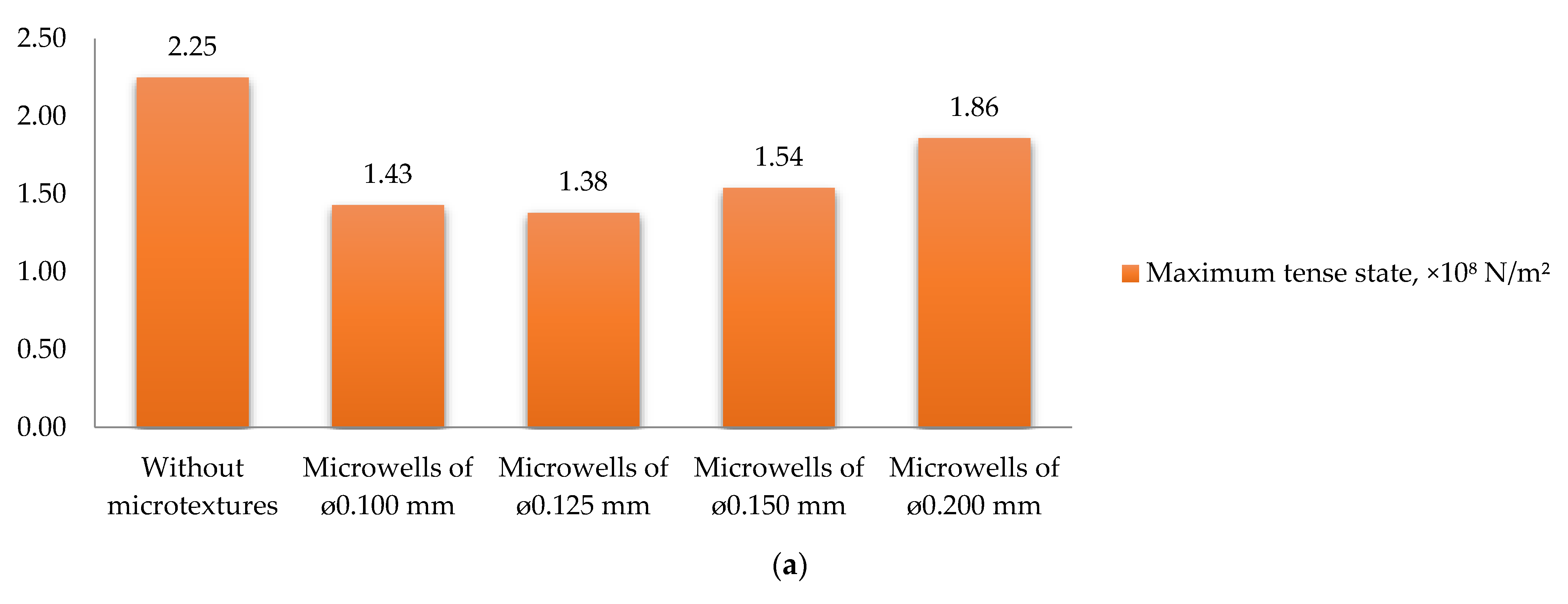
| Without microtextures | 2.25 × 10⁸ | 0.00074 |
| Straight microgrooves | 7.1 × 10⁸ | 0.00246 |
| Wavy microgrooves | 1.21 × 10⁹ | 0.00260 |
| Lattice microtexture, 3 × 3 | 8.66 × 10⁹ | 0.00977 |
| Microwells of ø0.100 mm | 1.43 × 10⁸ | 0.00083 |
| Microwells of ø0.125 mm | 1.38 × 10⁸ | 0.00056 |
| Microwells of ø0.150 mm | 1.54 × 10⁸ | 0.00068 |
| Microwells of ø0.200 mm | 1.86 × 10⁸ | 0.00616 |
| Cutting Time, min | Wear Chamfer on the Flank Face of TiN-Coated Si3N4 Cutting Inserts, µm | ||
|---|---|---|---|
| Without Microtextures | Straight Microgrooves, z = 0.210 mm | Microwells, d = 0.080 mm | |
| 2 | 183.20 ± 3.00 | 122.60 ± 3.00 | 156.20 ± 3.00 |
| 4 | 282.80 ± 3.00 | 219.50 ± 3.00 | 189.80 ± 3.00 |
| 6 | 348.30 ± 3.00 | 305.20 ± 3.00 | 257.10 ± 3.00 |
| 8 | 418.50 ± 3.00 | 342.70 ± 3.00 | 286.30 ± 3.00 |
| 10 | 612.90 ± 3.00 | 421.50 ± 3.00 | 327.60 ± 3.00 |
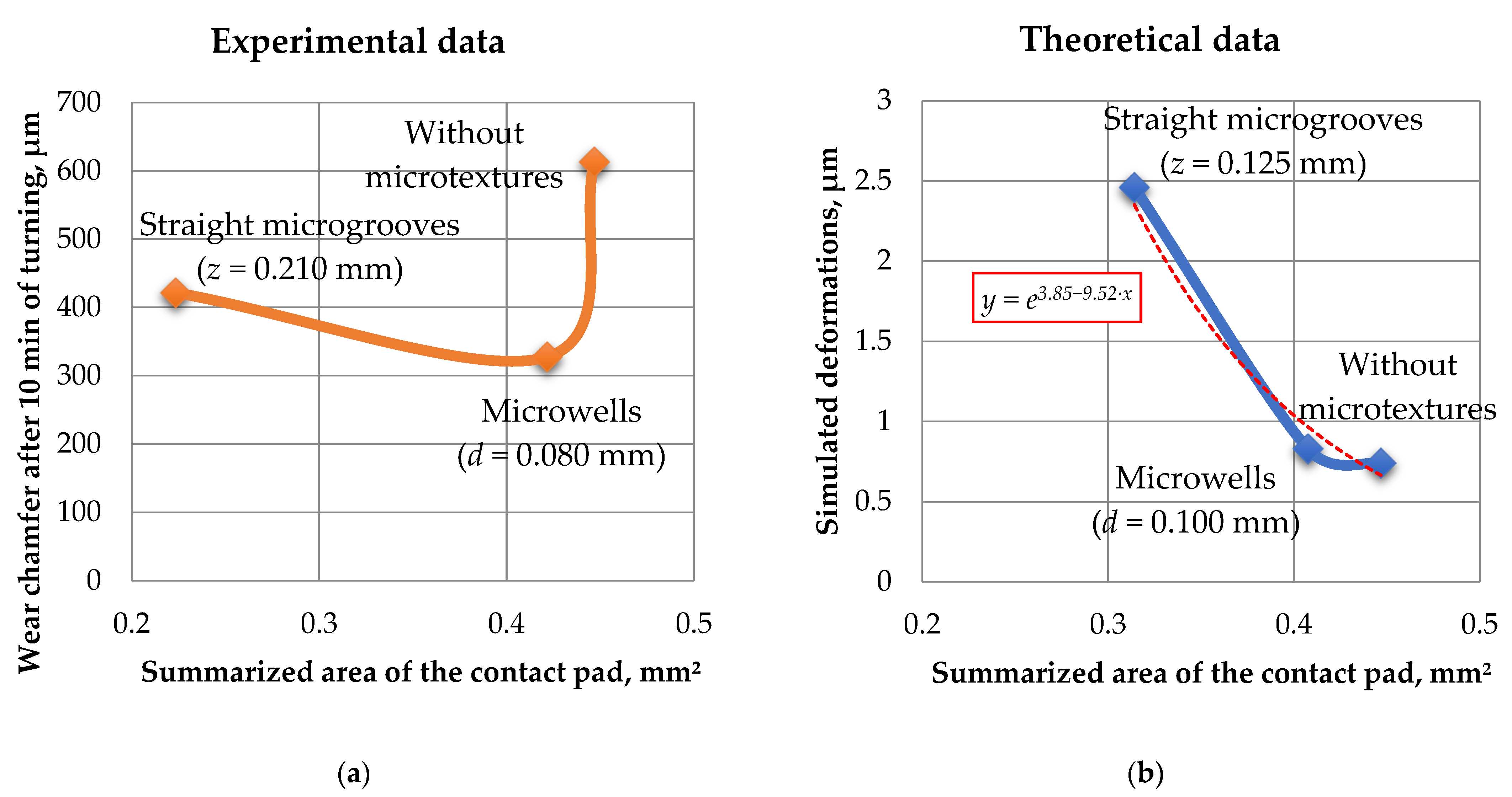
| Type of Cutting Insert | Experimental Data | Theoretical Data | |
|---|---|---|---|
| Wear Chamfer after 10 min of Turning, µm | Tense State, N/m2 | Deformations, µm | |
| Without microtextures | 612.90 ± 3.00 | 2.25 × 10⁸ | 0.74 |
| Straight microgrooves | 421.50 ± 3.00 (z = 0.210 mm) | 7.1 × 10⁸ | 2.46 (z = 0.125 mm) |
| Microwells | 327.60 ± 3.00 (d = 0.080 mm) | 1.43 × 10⁸ | 0.83 (d = 0.100 mm) |
| Cutting Insert | Coating | Microtexture | Method of Production | Workpiece Material | Turning Condition | Performance Effect | Reference |
|---|---|---|---|---|---|---|---|
| Si3N4, square-shaped | TiN coating of 3.8–4.0 µm | 3 lines of 9 microwells of ø80 µm, at a distance of 150–175 µm from the cutting edge | Electrical discharge drilling with a tungsten wire of ø100 µm in TiO2-powder suspension (150 g/L) | XH45MBTJuBP (C0.1Cr15Ni45Mo4.6Mn0.6Fe) nickel-based heat-resistant alloy | V = 300 m/min, s = 0.5 mm/rpm, t = 0.5 mm, no lubricant, Tmax = 900 °C | Increased the durability by 1.3 times | Current study |
| TK20 carbide alloy, square-shaped | Multilayer nATCRo3 coating ((CrTi)N/(AlTi)N layers alternation + (AlTiCr)N/SiN nanocomposite layer where (AlTiCr)N crystals in amorphous Si3N4) | 4 lines of doubled square-shaped prints with a width of 30 µm, a depth of 7 µm, at a distance 181 µm from the cutting edge | Nanoindentation (plastic deformation) with a force of 20 N | C0.3Cr15Ni35Mo7Mn7Fe iron–nickel heat-resistant alloy | V = 17–27 m/min, s = 0.1–0.15 mm/rpm, t = 0.3–0.5 mm, MoS2-based lubricant, Tmax = 240–330 °C | Increased the durability by 1.3–1.5 times | [9] |
Disclaimer/Publisher’s Note: The statements, opinions and data contained in all publications are solely those of the individual author(s) and contributor(s) and not of MDPI and/or the editor(s). MDPI and/or the editor(s) disclaim responsibility for any injury to people or property resulting from any ideas, methods, instructions or products referred to in the content. |
© 2023 by the authors. Licensee MDPI, Basel, Switzerland. This article is an open access article distributed under the terms and conditions of the Creative Commons Attribution (CC BY) license (https://creativecommons.org/licenses/by/4.0/).
Share and Cite
Volosova, M.A.; Okunkova, A.A.; Hamdy, K.; Malakhinsky, A.P.; Gkhashim, K.I. Simulation of Mechanical and Thermal Loads and Microtexturing of Ceramic Cutting Inserts in Turning a Nickel-Based Alloy. Metals 2023, 13, 1241. https://doi.org/10.3390/met13071241
Volosova MA, Okunkova AA, Hamdy K, Malakhinsky AP, Gkhashim KI. Simulation of Mechanical and Thermal Loads and Microtexturing of Ceramic Cutting Inserts in Turning a Nickel-Based Alloy. Metals. 2023; 13(7):1241. https://doi.org/10.3390/met13071241
Chicago/Turabian StyleVolosova, Marina A., Anna A. Okunkova, Khaled Hamdy, Alexander P. Malakhinsky, and Khasan I. Gkhashim. 2023. "Simulation of Mechanical and Thermal Loads and Microtexturing of Ceramic Cutting Inserts in Turning a Nickel-Based Alloy" Metals 13, no. 7: 1241. https://doi.org/10.3390/met13071241