Article

Lattice Dynamics, Transport and Thermoelectric Properties of Bi-Sb Alloys Obtained by Mechanical Alloying and Spark Plasma Sintering

1
ICGM, Univ Montpellier, CNRS, ENSCM, Montpellier, France
2
L2C, Univ Montpellier, CNRS, Montpellier, France
3
ICMPE, Univ Paris-Est, CNRS, Thiais, France
4
ICMMO, Univ Paris Saclay, CNRS, Orsay, France
*
Author to whom correspondence should be addressed.
Metals 2024, 14(1), 40; https://doi.org/10.3390/met14010040
Submission received: 24 November 2023 / Revised: 26 December 2023 / Accepted: 27 December 2023 / Published: 29 December 2023
(This article belongs to the Section Powder Metallurgy)

Abstract

:
We report on the successful synthesis of Bi1−xSbx alloys via mechanical alloying followed by sintering via spark plasma sintering, and the study of their lattice dynamics by Raman spectroscopy as well as their transport and thermoelectric properties. We observed an upshift of the frequency of the Raman-active Eg vibrational mode with increasing Sb content but no significant change for the frequency of the Raman-active A1g vibrational mode. Conversely, the linewidth of the Eg vibrational mode did not change significantly with increasing Sb content, whereas a twofold increase was observed for the A1g vibrational mode. Moreover, we confirm the emergence of several new vibrational modes with Sb alloying that could be associated with Bi-Sb and Sb-Sb vibrations. Rather large magnetoresistance was observed for all samples at room temperature. From the Seebeck coefficients, we determined the energy bandgaps in our samples, which are larger than those in bulk compounds, presumably due to the electronic confinement effect. We report a rather large thermoelectric power factor of 2–3 mW/m.K2 and thermoelectric figure of merit ZT of 0.15–0.23 at room temperature. However, ZT values were not improved at room temperature compared to prior works because of the rather large thermal conductivity of 3.75–4.5 W/m.K at room temperature. We find a larger resistivity, Seebeck coefficient, and power factor for the samples sintered at 200 °C for 5 min than for the samples sintered at 220 °C for 15 min, but similar thermal conductivity, resulting in larger ZT for the samples obtained in the first conditions. The samples with low Sb content x = 0.05 have a lower power factor and larger thermal conductivity than the samples with x = 0.12 and x = 0.15 for the same sintering conditions, which results in lower ZT for x = 0.05.

1. Introduction

Among thermoelectric applications, solid-state cooling and thermal management taking advantage of the Peltier effect are the most widely used to date [1]. Peltier cooling has many advantages compared to vapor compression cooling systems, such as the absence of chemical fluids, very good reliability, size compactness, absence of noise, capability of rapid cooling or heating, and very precise control of temperature. However, it still has low coefficient of performance (COP) compared to the COP of vapor compression refrigerators [1]. The COP of Peltier refrigerators is related to the dimensionless thermoelectric figure of merit ZT of the materials that comprise the thermoelectric modules, which is defined as ZT = S2σT/κ, with S being the Seebeck coefficient, σ being the electrical conductivity, T being the temperature, and κ being the thermal conductivity [1,2].
Until recently, the best thermoelectric materials for Peltier cooling applications around room temperature, and those used nowadays, are Bi2Te3−xSex (n-type) and Bi2-xSbxTe3 (p-type) alloys [1]. They both exhibit ZT values larger than 0.5 above about 200 K [1]. To date, two materials have been obtained with larger ZT values above 100 K in the case of the n-type material Mg3Bi1.25Sb0.75 and below 250 K in the case of the p-type material CsBi4Te6 [1]. The n-type Bi0.905Sb0.095 alloys have larger ZT than Bi2Te3-xSex below 200 K and Mg3Bi1.25Sb0.75 below 175 K [1]. In the case of Bi1−xSbx alloys, the best ZT obtained at low temperature was about 0.5 at 70 K for x = 0.15, in the case of n-type doping [3]. However, p-type doping is much less efficient for Bi1−xSbx alloys and a maximum ZT = 0.12 or 0.13 was reached at 240 K for (Bi1−xSbx)1−ySny alloys with x = 0.225 doped with 0.75% of tin [4] or with x = 0.15 doped with 2.5% of tin [5]. For both n-type and p-type Bi1−xSbx alloys, the application of a magnetic field increases the ZT values at low temperature [6]. Yim and Amith found a ZT of 1.1 at 100 K with a magnetic field of 0.3 T in the case of n-type Bi0.85Sb0.15 alloys and a ZT of about 0.2 at 85 K and 0.75 T for p-type Bi0.88Sb0.12 doped with 300 ppm of tin [6]. At 70 K, the best thermoelectric properties of n-type Bi1−xSbx alloys are observed in their semiconducting domain for 0.07 < x < 0.22, whereas at room temperature the ZT is slightly larger in the semimetallic domain, for x ≤ 0.07, which is similar to elemental Bi [3,6]. In fact, Kane and coworkers demonstrated theoretically that the Bi1−xSbx alloys are strong topological insulators for 0.07 < x < 0.22, i.e., they possess topologically protected metallic surface states within the bulk energy bandgap of a few 10 meV [7,8]. This feature was experimentally confirmed using angle-resolved photoelectron spectroscopy (ARPES) by Hsieh et al. [9,10]. Later, Nakamura et al. observed a topologically nontrivial edge state for x = 0.04 [11], which was thought at this time to be the critical concentration where the bonding and antibonding bands at the L point are inverted [3]. Subsequently, other studies suggested that this transition appears at lower x, namely x = 0.023 [12] or x = 0.03–0.04 [13]. However, regardless of the actual value of the critical concentration, xcrit, Bi1−xSbx alloys are topologically trivial at xcrit, Dirac semimetals exist at xcrit, and topologically nontrivial semimetals exist above xcrit [12,13]. Additionally, there are also experimental indications of the presence of a Weyl semimetal around this critical concentration [13,14]. Several effects, such as the spin Hall effect [15] or intense spintronic THz emission [16], are related to these topological electronic structures.
When decreasing the dimensionality, topological transitions occur, and the energy bandgap opens for all Sb concentrations below a critical thickness in the case of thin films, or a critical diameter in the case of nanowires, of tens nanometers in both cases [15,17,18]. This effect, linked to quantum confinement as well as to the increase in phonon scattering by multiple interfaces, underlines the interest in reducing the dimensionality of the materials in order to potentially improve the thermoelectric performances of the Bi1−xSbx alloys. Besides very thin films and nanowires, the design of bulk samples with grains of nanometer size could constitute a promising direction. This strategy was previously followed, notably in the case of Bi2Te3-based alloys synthesized by mechanical alloying and for which ZT was increased by about 40% up to 1.4 at 100 °C [19]. In the case of Bi1−xSbx alloys, because of the large difference in the melting temperature of Bi and Sb, the standard melting method can result in severe segregation of Sb within the samples, leading to heterogeneous composition [3]. Powder metallurgy methods such as mechanical alloying are a way to solve this problem and obtain homogeneous samples, as shown by Martin-Lopez et al. [20]. Another metallurgical method can also be used, i.e., melt spinning [21,22]. To date, some other methods have been used to obtain very small grain size, such as arc plasma processing [23], wet chemical synthesis processing with the polyol route [24], the chemical solution route [25], the solvothermal method [26], or the sonoelectrochemical technique [27]. Among the four latter bottom-up methods, only Kaspar et al. studied the thermoelectric properties of a Bi0.85Sb0.15 alloy densified with spark plasma sintering [24]. Devaux et al. studied the thermoelectric properties of a Bi0.865Sb0.135 alloy after cold pressing, eventually followed by pressureless sintering, and observed degraded ZT values for the samples with 100 nm grain size [28], but this degradation could be due to the low density of the pellet. Mechanical alloying has been the main technique used for nanostructuring Bi1−xSbx alloys [5,20,29,30,31,32,33,34,35,36,37,38,39,40,41,42,43,44,45,46,47]. In some works, it was shown that grain size of about 30–100 nm can be obtained by mechanical alloying [34,38,39,40]. However, for the densification of the powder into pellets, most of these works used hot pressing or cold pressing followed by pressureless sintering [29,30,33,34,37,38,39,40,41,43]. However, these methods result in a competition between grain coarsening and densification, and the nano grain size is not preserved in the case of high-density pellets. In order to limit or even avoid grain coarsening, a very high pressure of 5 GPa has been used by Liu et al. [32]. Spark plasma sintering, as it involves a short heating time and the use of a much smaller pressure of tens MPa, has been used for many families of materials to obtain high-density pellets while preserving nano-size grains. SPS was first used for direct reaction between Bi and Sb powders having a micrometer size to obtain Bi0.91Sb0.09 alloy by Lee and Koyanagi in 2001 [48]. SPS was also used for shaping Bi1−xSbx alloys obtained by melt spinning [21,22]. SPS was used in a limited number of studies devoted to mechanically alloyed powders of Bi1−xSbx alloys [35,36,42,44]. Chen et al. found that such samples after SPS have a grain size of 200 nm [36]. Almost all the works reporting the thermoelectric properties of Bi1−xSbx alloys obtained by mechanical alloying focused on Sb content in the range 10–15% [5,20,30,31,32,33,34,35,36,37,42,43,44], corresponding to the semiconducting compositions with a direct bandgap [3,17]. In contrast, some groups explored compositions with x > 0.15 [38,39,40,41], whereas Günes et al. reported on the thermoelectric properties of two samples with x < 0.1 at room temperature [37] and Miyajima reported the thermoelectric properties for a sample with x = 0.075 at room temperature [29]. Therefore, it would be interesting to explore such low Sb compositions as a function of the temperature. Despite the interest in exploring the thermoelectric properties between room temperature and 100 °C for thermal management and air-conditioning applications, this temperature range has been investigated only by Dutta et al. [37] and Asfoury et al. [43,44,45,46] in the case of samples obtained by mechanical alloying. There is also only a single study on magnetotransport properties in samples obtained by mechanical alloying [44], and no study at all on lattice dynamics.
Therefore, the main aim of the present work is to fill these gaps. We studied several Bi1−xSbx alloys obtained using mechanical alloying followed by SPS, with compositions x = 0.05 corresponding to the topologically nontrivial semimetal, as well as x = 0.12 and x = 0.15 corresponding to the direct bandgap semiconductors. After the structural characterization, we report, for the first time, the Raman scattering experiments and magnetotransport experiments at room temperature on Bi1−xSbx alloys obtained after both mechanical alloying and SPS. Finally, we report the thermoelectric properties in the 30–100 °C range for these different Bi1−xSbx alloys obtained by mechanical alloying and SPS, and, for the first time, for the sample x = 0.05.

2. Materials and Methods

2.1. Sample Preparation

Bi1−xSbx alloys were obtained by mechanical alloying using stoichiometric amounts of pre-ground pieces of Bi 5N and Sb 5N for alloys with x = 0.05, 0.12 and 0.15. Mechanical alloying was performed using a planetary “pulverisette 7” micromill from Fritsch GmbH–Milling and sizing (Idar-Oberstein, Germany) within an Ar-filled glove box, with a stainless steel jar of 45 mL with 5 stainless steel balls of 10 mm diameter. The ball-to-powder mass ratio was 10:1, the rotation speed was 350 rpm, and the grinding duration was 24 h of effective time with an alternative sequence of 15 min of milling and a 15 min pause to limit the heating during mechanical alloying. For the thermoelectric properties, Bi1−xSbx powders were shaped into pellets of 8 mm diameter via spark plasma sintering (SPS) using a DR Sinter Lab 515S from Fuji Electronics Industrial Co (Saitama, Japan). The powder was loaded within an Ar-filled glove box in a graphite die of 8 mm diameter. The samples were pressed under 100 MPa and heated at 200 °C for 5 min (samples A) or 220 °C for 15 min (samples B).

2.2. Sample Characterization

For the X-ray diffraction experiments, the powder obtained from mechanical alloying was put in a sample holder isolated from the atmosphere by Kapton foil and loaded with an Ar-filled glove box, whereas the pellets obtained from SPS were polished using SiC polishing paper to remove the graphite at the surface, prior to the experiments. We used a D8 Bruker diffractometer equipped with a Johansson monochromator to obtain only the Kα1 Cu wavelength (1.5406 Å). The powder patterns was analyzed using Rietveld refinement (for the powders obtained after mechanical alloying) or pattern matching (for the pellets) using the Fullprof 64 bits software [49]. We attempted to determine the grain size using the Williamson–Hall method, which is implemented in Fullprof. The apparent density dapp of the pellets was determined using the Archimedes technique using ethanol as solvent. The density d was obtained from the ratio between the apparent density dapp of the pellets and the density dXRD obtained from the pattern matching of the XRD powder patterns. For all the samples, the density d was higher than 99%. The actual stoichiometry of the pellets obtained by SPS was determined via chemical analysis using electron dispersive X-ray spectroscopy (EDXS). Prior to the experiments, the samples were polished with alumina powder of 1 µm diameter. The experiments were carried out using an X Max N SDD detector from Oxford instruments within an EVO HD15 scanning electron microscope from Zeiss. The Bi and Sb contents were obtained from the statistical average of 8 points for each sample and the uncertainty was obtained from the standard deviation. Raman scattering experiments were performed using a T64000 spectrometer from Horiba France SAS (Palaiseau, France) equipped with nitrogen-cooled CCD in a triple-monochromator configuration in order to probe Raman-active modes down to 50 cm−1. We used a laser having a 660 nm wavelength from Cobolt with spectral resolution of 2 cm−1. In order to avoid sample heating, we used a power of 0.3 mW. The Seebeck coefficient was measured up to 120 °C using a homemade experiment. The thermal gradient was established by heating the sample on one side with a light, and the temperature and voltage were obtained using Chromel and Alumel thermocouples. The electrical resistivity was measured with the van der Pauw technique up to 120 °C with a homemade experiment. The room temperature Hall effect and transverse magnetoresistance were measured under a magnetic field up to 1 T with the van der Pauw technique in another homemade experiment. The thermal conductivity was obtained from the relation κ = DdappCp, with D being the thermal diffusivity, dapp being the apparent density of the pellets, and CP being the heat capacity. The thermal diffusivity D was measured via the laser flash technique using a LFA 457 Microflash apparatus from Netzsch (Selb, Germany). The heat capacity CP was measured on samples sintered at 200 °C during 5 min from 50 °C to 140 °C via differential scanning calorimetry (DSC) with a DSC 404 C Pegasus apparatus from Netzsch and using the ratio method. We used the results of these experiments only for the composition x = 0.15, because for the other compositions we used the heat capacity data between room temperature and 125 °C from Rogocheva et al. [50], who measured accurate heat capacity between −100 °C and 250 °C for the compositions x = 0.055 and x =0.12.

3. Results

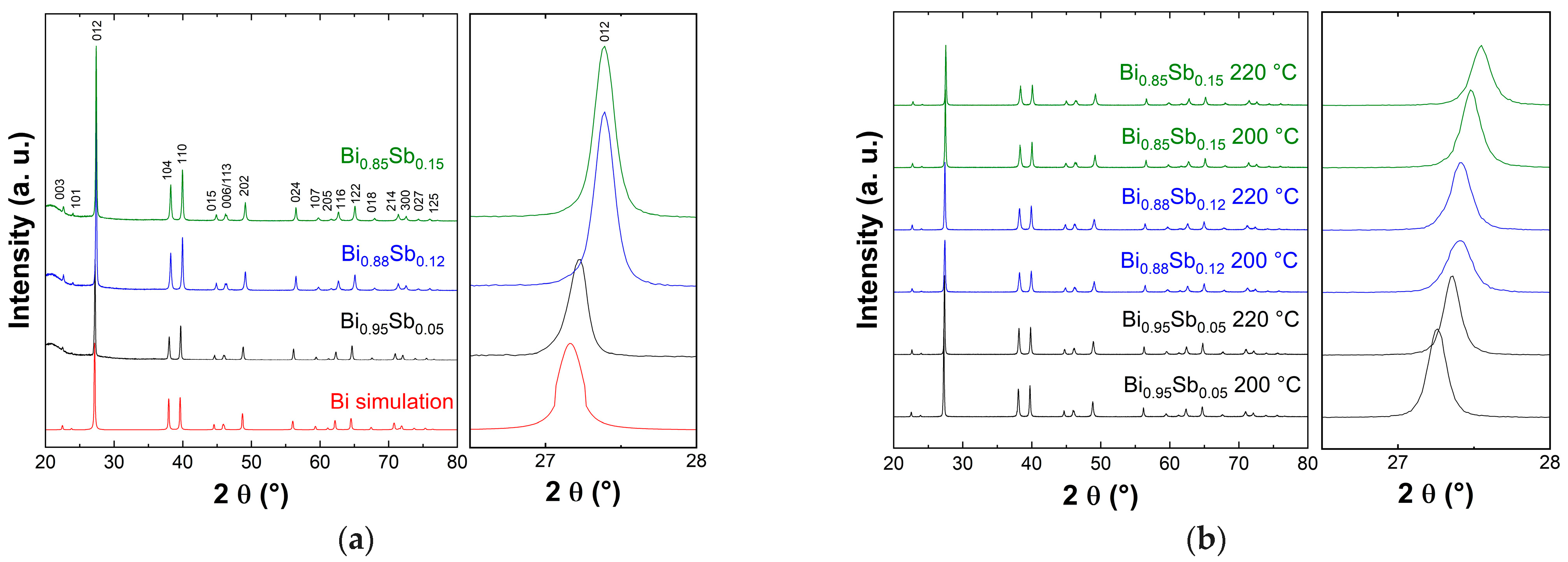
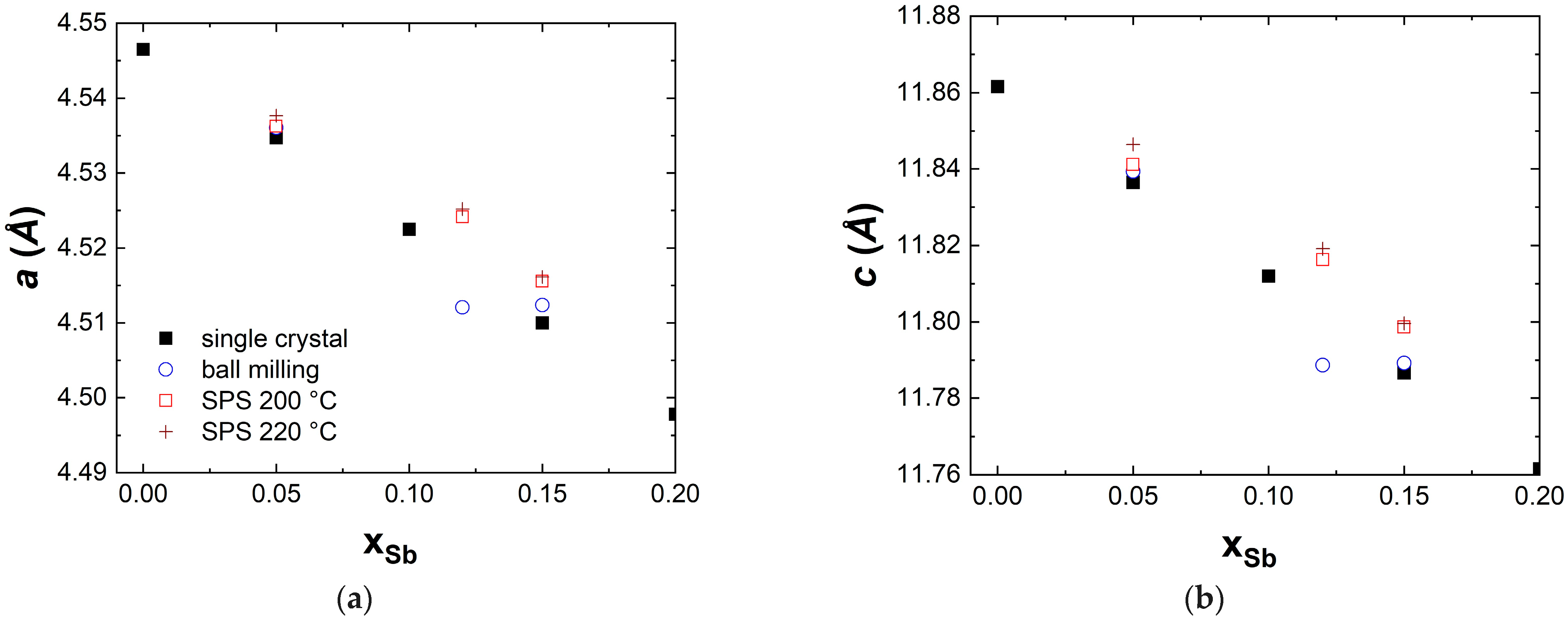
3.1. Structural Characterization

XRD patterns of the Bi1−xSbx alloys obtained after mechanical alloying are plotted in Figure 1a, and after SPS at 200 °C or 220 °C in Figure 1b. After mechanical alloying, the observed Bragg peaks can be attributed to the rhombohedral crystal structure of Bi with a slight shift to larger angles due to alloying of Bi with Sb, which results in lower lattice parameters, as confirmed by Rietveld refinement. No other peaks can be observed, indicating that all the Sb reacted with Bi, resulting in single-phase samples within the detection limit of XRD. Note that the bump at a low angle in Figure 1a is due to the Kapton foil used to protect the powdered sample from air. The broadening of the peaks is related to the decrease in the crystallite size to about 100 nm, as determined by Rietveld refinement for the sample with x = 0.05. However, we were not able to determine the crystallite size for the two samples with x = 0.12 and 0.15, even though they have similar linewidth. After SPS, all the Bragg peaks can still be attributed to the Bi1−xSbx alloys and the samples are single phase.
The lattice parameters obtained from Rietveld refinement (for the powders obtained after mechanical alloying) and from pattern matching (for the pellets) are reported in Figure 2. Unfortunately, it was not possible to determine the crystallite size for the SPS pellets from the pattern matching. Our results for the samples after mechanical alloying and SPS are compared with the work of Dismukes et al. on crushed single-crystalline bulk samples [51]. In the case of mechanically alloyed samples, the lattice parameters a and c are only slightly larger than those from bulk for x = 0.05 and x = 0.15 but, unexpectedly, the lattice parameters for x = 0.12 are the same as those for x = 0.15 and lower than those in the bulk sample. One possible explanation for this could be an incomplete reaction during mechanical alloying, but after SPS, using these powders, which was completed after the SPS process; thereafter, the lattice parameters decreased almost linearly with increasing Sb content. The lattice parameters of the SPS samples are very close for the samples sintered at 200 °C and 220 °C. They are systematically larger than in the bulk samples and also than for the mechanically alloyed samples. This can be partially explained, mainly for the samples with nominal Sb content of 12%, by the results of our chemical analysis, as shown in Table 1. However, even with the Sb content from chemical analysis, the lattice parameters of our samples are still larger than those in the bulk samples. It must be noted that larger lattice parameters were found in mechanically alloyed samples than in bulk samples with 0.1 ≤ x ≤ 0.2 by Schlecht and coworkers [38,39]. Additionally, larger lattice parameters were also found in polycrystalline samples by Malik et al. [52] than by Dismukes et al. [51], and these were also larger than those in our present work. In contrast, Devaux et al. found smaller lattice parameters [28].

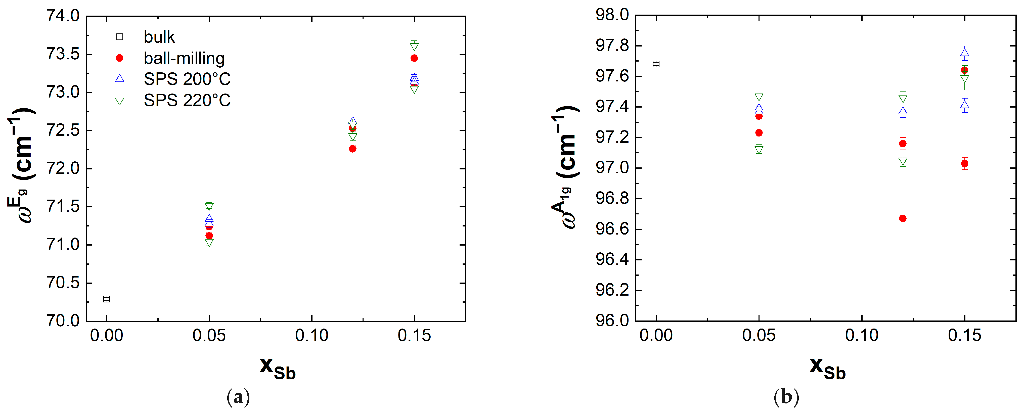
3.2. Raman Scattering

Rhombohedral Bi and Sb and their solid solution have two atoms per primitive unit-cell, and thus six vibrational modes. Their vibrational selection rules indicate that they have two Raman-active modes of A1g and Eg symmetries [53]. The Raman spectra of the Bi1−xSbx alloys obtained after mechanical alloying and after SPS at 200 °C and 220 °C are plotted in Figure 3. For comparison, we also measured the Raman spectrum of bulk Bi, for which we found vibrational frequencies at 70.3 cm−1 for the Eg mode and 97.7 cm−1 for the A1g mode, in good agreement with prior results from the literature [53,54,55,56].
When alloying Bi with Sb, the frequency of the Eg mode increases with Sb content, whereas the frequency of the A1g mode does not change significantly compared to the experimental resolution (see Figure 4). The frequency of the Eg mode increases although the volume of the unit cell decreases with Sb content, in contrast with the evolution observed under pressure where it was found to decrease with increasing pressure, and therefore with decreasing volume [53,56]. This means that this increase in the frequency of the Eg mode is mainly due to the presence of the lighter Sb atoms and to an increase in the force constants with Sb alloying, as suggested by Lannin [55], and not to “chemical pressure”.
In the early works during the 1970s, Lannin also observed a slight increase in Eg mode frequency in the case of polycrystalline thin films [55], in contrast with Zitter and Watson, who did not find any clear trend at low Sb content when studying single-crystalline samples [53]. Both studies also reported no clear trend for the frequency of A1g at low Sb content, but a very small decrease with increasing Sb content at larger Sb content [54,55]. In more recent works, Sultana et al., in the case of single crystals [57], and Zhao et al., in the case of very thin 2D layers [58], also found an increase in the frequency of the Eg mode with Sb content having a similar magnitude as in our work. However, Sultana et al. found an increase in the frequency of the A1g with Sb content [56], in contrast with our work and the early studies [54,55]. We note that Kumar et al. [59] found lower frequencies for both modes in the case of Bi0.85Sb0.15 alloys than in our work and in other works. This might be explained by the heating of the sample due to too large laser power used in their experiments. It is more difficult to explain why Lee et al. found a slightly larger frequency of the Eg mode and a slightly smaller frequency of the A1g mode in the case of a single-crystalline sample with x = 0.04 [60] than for our x = 0.05 sample.
In Figure 5, we report the full-width at half maximum (FWHM) Γ of the two Raman-active modes Eg and A1g. Our work is the first to report the variation in FWHM of the Bi-Sb alloys of both Raman-active modes in detail. For bulk Bi, the linewidth is about two times broader for the Eg mode than for the A1g mode. This is in agreement with Olijnyk et al. [56] and Höhne et al. [61], who worked on bulk Bi and found a rather similar FWHM, but in contrast with the results of Lu et al. who worked on thin film of Bi [62]. We found that the FWHM of the Eg mode did not change significantly with Sb alloying, as also found by Zhao et al. in the case of 2D layers of Bi1−xSbx for x ≤ 0.15 [58]. This was also the case for bulk Bi0.9Sb0.1 compared to the Bi reference in Lannin’s work [55] if we examine their Raman spectra in detail. Therefore, both alloying and nanostructuring have no significant effect on the FWHM of the Eg mode. In contrast, the FWHM of the A1g mode increases with Sb alloying up to a factor of 2 for x = 0.15. At the present stage, it is difficult to say if the increase in the FWMH is due to nanostructuring or Sb alloying, or even both.
The most striking effect of the Sb alloying on Raman spectra is the emergence of additional peaks at about 110 cm−1 and 120 cm−1 for x = 0.05, and about 140 cm−1 for x = 0.12 and x = 0.15. Note that the intensity of the peak at about 140 cm−1 increases with the Sb amount, which means that it could also be possibly present, but hidden in the background, for x = 0.05. Zitter and Watson also observed some additional peaks in the Raman spectra of Bi1−xSbx alloys, which cannot be explained by a usual model of random atom substitution [54]. They found two additional peaks at about 125 cm−1 and at about 140–145 cm−1 for x = 0.05 and x = 0.12, and one third additional peak at about 115 cm−1 from x = 0.28 [54]. They attributed the peaks at 115 cm−1 and 140–150 cm−1 to Sb-Sb vibrations because they were close to the frequencies of the vibrations of pure Sb [54]. Lannin also observed additional peaks when alloying Bi with Sb but at 121 cm−1 and 146 cm−1, together with a shoulder at 114 cm−1 for x = 0.1 [55]. The values at low frequency are closer to our results for x = 0.12 and 0.15. Our results thus agree well with Lannin’s work [55]. Thus, in addition to the two lowest energy modes close to those of Bi due to Bi-Bi vibrations, and the two modes at about 114 cm−1 and 140–150 cm−1 due to Sb-Sb vibrations, Lannin attributed the fifth peak at about 120 cm−1 to Bi-Sb vibrations with A1g symmetry, i.e., to local mode vibration of Sb atoms surrounded by Bi atoms as first neighbors [55]. In the more recent works, Sultana et al. also observed only additional peaks at about 120 cm−1 and 140 cm−1 [55], whereas Zhao et al. observed only these peaks for x ≤ 0.18 and all the five peaks only for x ≥ 0.27 [56], and Lee et al. observed only one weak additional peak at about 118 cm−1 in their sample with x =0.04 [60]. In contrast, in our samples, we observed the peak at around 110 cm−1 even for low Sb content, and it is located at lower frequencies than in single-crystalline samples [54,55] and the same frequency as in the 2D layer of Bi0.65Sb0.35 studied by Zhao et al. [58]. These differences are probably due to the small grain size and/or disordering in our samples.

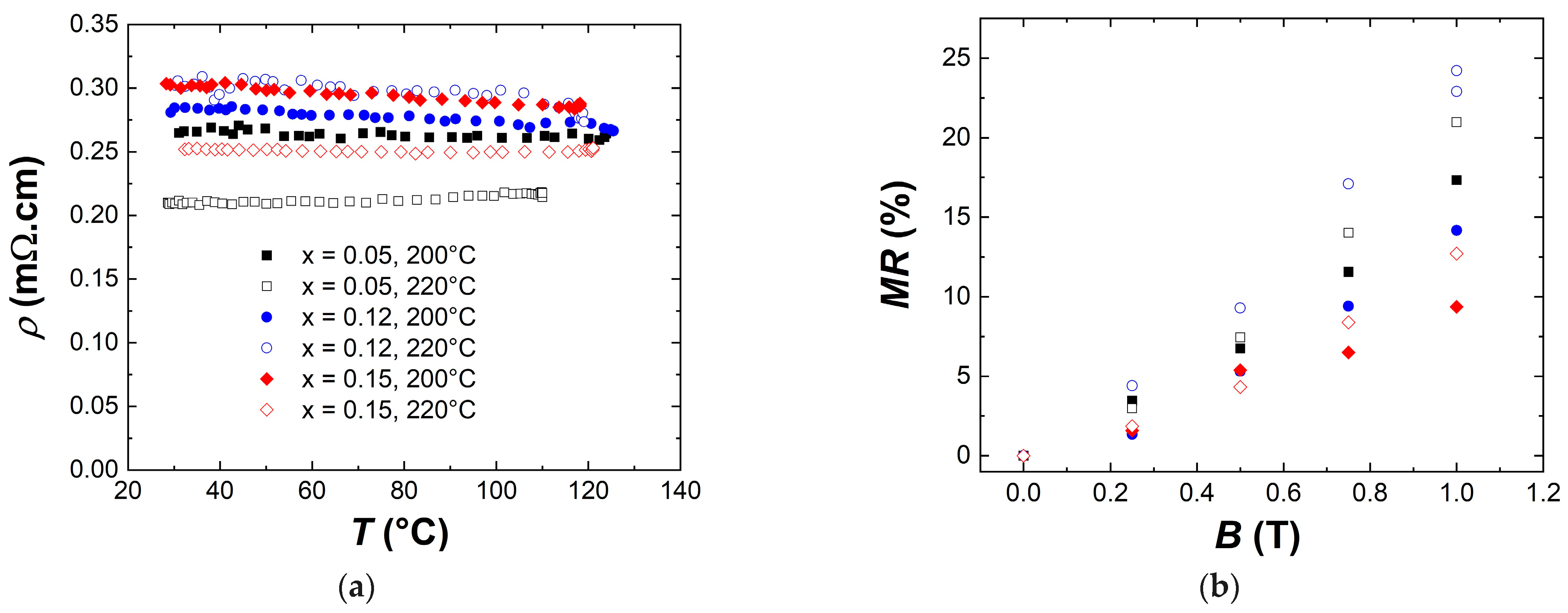
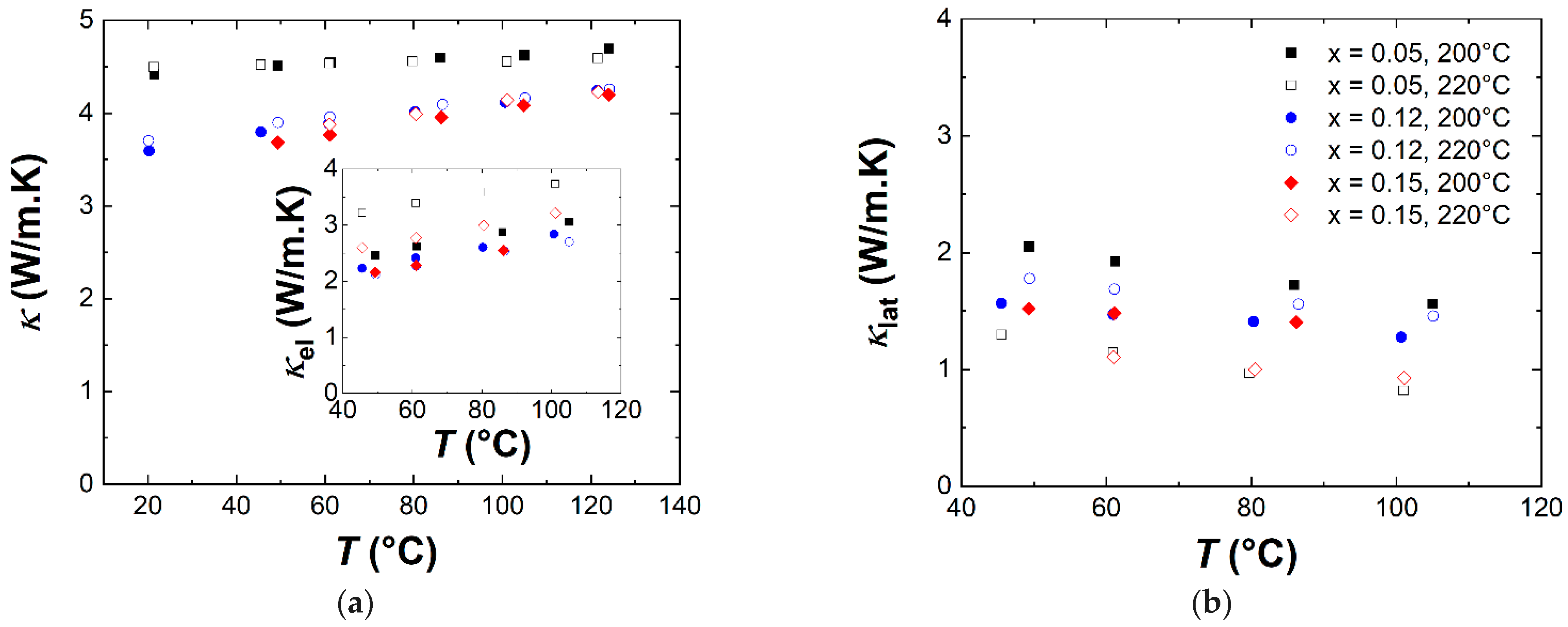
3.3. Transport and Thermoelectric Properties

The temperature dependence of the electrical resistivity for the different Bi1−xSbx samples is plotted in Figure 6a. The electrical resistivity values range between 0.2 and 0.3 mΩ.cm. At room temperature, these values are about two times larger than in the Bi1−xSbx single-crystalline samples [6,63], but they are comparable to those of polycrystalline samples obtained by conventional solid-state reaction in the Sb content range x = 0.1–0.15 [52]. In the literature, most of the samples obtained from mechanical alloying and hot pressing or very high pressure sintering with composition x = 0.1–0.15 have larger resistivity, in the range 0.45–0.8 mΩ.cm [5,32,33,38,39,40,43,47], or even larger than 1 mΩ.cm [37,46]. This could be related to a lower density than in our sample or/and a different level of doping. Martin-Lopez obtained only a slightly larger or similar resistivity [30]. Rodriguez obtained resistivity of x = 0.15 samples increasing from 0.2 to 0.4 mΩ.cm with increasing milling time from 5 h to 45 h, but they did not give the sintering method they used to densify their samples [31]. El-Asfoury observed resistivity of 0.235 mΩ.cm for samples with x = 0.15, slightly smaller than in our samples, but it will be seen latter that they also found much smaller thermopower than in our samples [45]. Günes et al. found smaller resistivity of about 0.33 mΩ.cm for x = 0.05 compared to the samples with higher Sb content [40], but which is larger than in our samples with x = 0.05. When examining the resistivity of SPS-densified samples for the range x = 0.1–0.15 in the literature, the values are close to our results [35,36,42,44]. Specifically, Flores-Conde et al. found a resistivity of about 0.3–0.4 mΩ.cm [42]. As the density values of these samples are similar to those of our samples, this could be related to different levels of doping, crystallinity, or interface defects between grain boundaries.
The resistivity of our sample x = 0.05 densified at 220 °C slightly increases with increasing temperature and is smaller compared to the other compositions. This is not surprising as Bi1−xSbx alloys are expected to be semimetallic for x ≤ 0.07 [3]. The electrical resistivity also does not change with temperature for the sample x = 0.05 densified at 200 °C, or, even more surprisingly, for the sample x = 0.15 densified at 220 °C, which was expected to exhibit a semiconducting behavior. For the other samples, the resistivity decreases with increasing temperature, as expected for semiconducting Bi1−xSbx alloys for 0.07 < x < 0.22 [3]. The difference between the resistivity values of the samples densified at 200 °C and those densified at 220 °C (and also the Seebeck coefficient, as will be seen later) could be due to the differences in crystallinity of the pellets, as well as the interface defects between grain boundaries (as a reminder, all pellets have density above 99% of the theoretical value).
Yin and Amith [6] studied the magnetic field dependence of the thermoelectric properties of single-crystalline Bi1−xSbx alloys with the magnetic field perpendicular to the trigonal axis and the current or thermal gradient. They found both large magnetoresistance and magneto-Seebeck coefficients and proposed that this was because the electron mobility is higher than the hole mobility [6]. Teramoto et al. was able to explain the magnetic field dependence of the Seebeck coefficient using a three-band model and they showed that its magnetic field dependence increases with decreasing effective mass of the electrons [64]. The nanostructuring of the Bi1−xSbx alloys can result in modifying the electronic structure of these alloys, which will impact the magnetotransport properties, as will be studied below. We report the magnetic field dependence of the transverse magnetoresistance MR = (ρ(B) − ρ(B = 0)) × 100/ρ(B = 0) of our different Bi1−xSbx samples in Figure 6b. With a magnetic field of only 1 T, we observe a positive normal magnetoresistance in the range 10–25%, depending on the samples. We can see that the samples with x = 0.15 have the lowest magnetoresistance. This agrees with prior results on single-crystalline samples at a lower temperature, for which it was found that the transverse magnetoresistance decreased with the increased Sb alloying [6,56]. Yim and Asmith proposed that alloying would reduce carrier mobilities, which would result in a lower magnetoresistance. It could explain why we observe larger magnetoresistance for the samples sintered at 220 °C with 15 min dwell; a sintering at higher temperature with a longer dwell time should result in lower disorder and defect content, increasing the mobility, and so resulting in larger magnetoresistance. The variation is faster than linear but less than quadratic for all samples, and could follow Bn with n = 1.2–1.4. However, we cannot exclude the possibility of a quadratic dependence for a low enough magnetic field. In single-crystalline samples, Yin and Amith found a quadratic in a low magnetic field, and weaker field dependence approaching linear variation in a higher magnetic field [6]. Will et al. found very large transverse magnetoresistance at 30 K and up to 10 T in different Bi1−xSbx samples obtained by mechanical alloying and hot pressing [47]. For samples with x = 0.1 and 0.13, the field dependence below 1 T of their magnetoresistivity curves is similar to those observed in our samples. In their study, they were able to fit the magnetic field dependence of the magnetoresistivity and Hall coefficient up to 10 T with a three-band model [47] similar to the one used by Teramoto et al. for the magneto-Seebeck coefficient [64]. Below 1 T, they found that the Hall coefficient decreases as an absolute value by about 10–15% [47]. In contrast, our Hall effect measurements performed at room temperature evidence a linear behavior, which enables extraction of a Hall coefficient, as reported in the Table 1. We did not observe any clear trend between the different samples. Although it is not strictly applicable in the Bi1−xSbx alloys due to the multiband nature, we roughly estimated the electron concentration n from the Hall coefficient RH using the one-band model where n = 1/eRH, with RH being the Hall coefficient, for a comparison with previous results from the literature extracted using the same procedure for samples obtained by mechanical alloying [35,36,40,43,44]. We found the electron concentration n ranging from about 6.5 to 9 × 1018 cm−3. We also estimated the Hall mobility µ, which ranges from about 2300 to about 3800 cm2/V.s. Although these estimations should be seen as qualitative, it seems that our samples have a lower electron concentration and higher mobility than in previous works [35,36,40,43,44].
We report the temperature dependence of the Seebeck coefficient of the different Bi1−xSbx samples in Figure 7a. Two clear trends can be observed: the absolute value of the Seebeck coefficient of the samples sintered at 200 °C are always larger than those of the samples sintered at 220 °C; and, for each sintering condition, it increases from x = 0.05 to x = 0.12 and then decreases for x = 0.15. The Seebeck coefficient at room temperature of the sample with x = 0.05 is smaller than that in single-crystalline samples and in mechanically alloyed samples reported by Günes et al. [40]. For the samples in the range x = 0.12–0.15, our Seebeck coefficients at room temperature are comparable with those of single-crystalline samples [6,63], but they are smaller than in most of the previous studies of mechanically alloyed samples [5,30,33,34,35,36,40,42,44,46]. This is consistent with the larger resistivity in these samples, as discussed previously. This observation contradicts the previous analysis of the electron concentration from the Hall effect using a one-band model, which confirms the unsuitability of this model and the need to combine Hall effect and magnetoresistance experiments in a high magnetic field and to apply a three-band model, as conducted by Will et al. [47]. The Seebeck coefficient of the different samples follows a 1/T temperature dependence between 44–60 °C (depending on the samples) and 105 °C (see Figure 8a), as expected for the case of nondegenerate intrinsic semiconductor assuming parabolic bands and scattering of the charge carriers by acoustic phonons [31,65]. In this case, we can determine the energy bandgap through [65]:
S = k B e E g 2 k B T
where kB is the Boltzmann constant, e is the electron charge, and Eg is the energy bandgap.
We show our results in Figure 8b compared with prior results in the literature. We find a larger energy bandgap than in bulk single-crystalline samples [6,63]. However, for x = 0.05 we find results similar to those of Will et al. for hot-pressed samples using powder obtained by mechanical alloying [47] or of Cho et al. for thin films [65]. Our energy bandgap values are, however, significantly larger than in these last works for the samples x = 0.12 and 0.15. This increase in bandgap should be due to the electronic confinement induced by the small grain size of our samples, as it was also the case in the samples of Wille et al. [47]. We thus confirm their results of an increase in the energy bandgap in Bi1−xSbx alloys obtained from mechanical alloying.
The power factor of the different Bi1−xSbx samples is plotted in Figure 7b. At room temperature, it ranges between 2 and 3 mW/m.K2, and it decreases to about 1.5–1.75 mW/m.K2 at 100 °C. As in the case of the Seebeck coefficient, two clear trends are observed: the power factor values of the samples sintered at 200 °C are always larger than those of the samples sintered at 220 °C; and, for each sintering condition, the power factor increases from x = 0.05 to x = 0.12 and then decreases for x = 0.15. For the samples with x = 0.05 and at room temperature, we observe a power factor of 2 and 2.5 mW/m.K2 for the sample sintered at 220 °C and 200 °C, respectively, which is comparable to the value of about 2.1 mW/m.K2 found by Günes for hot-pressed samples from mechanically alloyed powders [40]. For the compositions x = 0.12 and x = 0.15, we found power factors of 2.5–3 mW/m.K2 at room temperature. These values are lower than those in single-crystalline samples [6,63] but larger than those in most previous works with mechanically alloyed samples [5,32,33,34,35,36,37,38,39,40,43,44,45,46], with the exception of the samples obtained by SPS by Flores-Conde et al. (2.75–3.7 mW/m.K2 at room temperature) [42] and the samples obtained by Martin-Lopez et al. (3.7–4 mW/m.K2 at room temperature) [30]. The main reason for this is the lower resistivity in our samples compared to most of these studies, as discussed previously.
The temperature dependence of the thermal conductivity of the different Bi1−xSbx samples is reported in Figure 9a. The samples x = 0.05 exhibit the largest thermal conductivity, close to 4.5 W/m.K, with flat temperature dependence. The other samples have lower thermal conductivities, with a weak increase from about 3.6 W/m.K around room temperature to 4.25 W/m.K at about 120 °C. The sintering conditions seem to have almost no influence on the thermal conductivity. In order to separate the electronic and the lattice contributions, we determined the electronic contribution κel using the Wiedemann–Franz law with the Lorenz factor L obtained in the single parabolic band approximation with acoustical phonon scattering [67]: L = (1.49 − 0.49 e−|S|/21 + 1.4 e−|S|/85)·10−8 W.Ω.K−2. The lattice contribution κlat was obtained after subtraction of the electron contribution κel from the measured thermal conductivity κ. We used the same procedure for the literature data in order to compare them with our results in a consistent way. As can be observed in Figure 8a,b, these contributions change significantly from one sample to the other. The electronic contribution is always the major contribution regardless of the temperature or the sample, and its contribution constitutes at least two-thirds of the thermal conductivity above 100 °C in all samples. For the same sintering conditions, the electronic contribution is always the largest for the semimetallic sample with x = 0.05 and explain the larger thermal conductivity compared to Sb-richer samples. The lattice contribution decreases with the temperature, as expected from the Umklapp scattering [2]. In the literature, most of the studies devoted to mechanically alloyed samples with x = 0.1–0.15 reported smaller thermal conductivity values at room temperature than in our samples [32,33,34,35,36,38,39,40,43,44,46], with the exceptions of the work of Dutta et al. [34], Chen et al. [5], and Martin-Lopez et al. [30]. This can be explained by the much smaller electronic contribution of the thermal conductivity in all these works as compared to our samples, in agreement with the lower resistivity in our samples, as discussed previously. Günes et al. [40] found quite similar thermal conductivity at room temperature for their samples with x = 0.05 than for our sample. After subtracting the electronic contribution to the total thermal conductivity in the same manner as in our case, in a few studies the lattice thermal conductivity for x = 0.15 is smaller [33] or even much smaller [32,35] than 1 W/m.K. However, in most cases, the lattice thermal conductivity values in the literature [34,38,39,40,44,45] are in, or close to, the range (1.3–1.8 W/m.K) of our x = 0.12 and x = 0.15 samples. In a few studies [5,46], the lattice thermal conductivity is larger than that in our samples. In the Martin-Lopez study [30], the extruded samples have slightly larger lattice thermal conductivity than in our samples, whereas the sintered samples have much larger lattice thermal conductivity. Finally, the x = 0.05 sample of Günes et al. has larger lattice thermal conductivity than our samples with the same Sb content. The low lattice thermal conductivity observed in our samples, which represents only 35% of the total thermal conductivity, shows that there is little room to decrease it more at high temperature in order to increase ZT. Therefore, the efforts to improve ZT at high temperature should rather focus on the power factor.
The temperature dependence of the thermoelectric figure of merit ZT of the different Bi1−xSbx samples is reported in Figure 10. As in the case of the power factor, ZT is smaller for the samples with x = 0.05, with a maximum value of about 0.15 close to room temperature. For this Sb content, ZT is only slightly decreasing with increasing temperature between 40 °C and 100 °C, whereas it decreases by about 15–20% for the samples with x = 0.12 and x = 0.15. The maximum ZT of about 0.23 is obtained close to room temperature for the sample x = 0.12 after sintering at 200 °C. For all the samples, we obtained a larger ZT around room temperature than Schlecht’s team [38,40] and in some other studies for x = 0.15 Sb content [36,37,43,46], but it is smaller than that in many studies [30,33,34,35,44], mainly due to the smaller Seebeck coefficient and larger thermal conductivity in our samples. Finally, we wish to underline that we find the same trend for the ZT variation with x at room temperature as Günes et al. [40], with smaller ZT for the sample x = 0.05 than for the samples with x > 0.1. This result contrasts with the prior findings for single-crystalline samples at room temperature where the inverse result was observed [3,6].

4. Conclusions

In the present work, we reported the successful synthesis of Bi1−xSbx alloys by mechanical alloying followed by sintering by SPS. The Raman spectroscopy experiments revealed an upshift in the frequency of the Eg vibrational mode with increasing Sb content but no significant change for the frequency of the A1g vibrational mode. Conversely, the linewidth of the Eg vibrational mode did not change significantly with increasing Sb content, whereas that of the A1g vibrational mode increases by a factor of two. Moreover, we confirm the emergence of several new vibrational modes with Sb alloying, which could be associated with Bi-Sb and Sb-Sb vibrations. The Raman line at 110 cm−1 appears at lower Sb content and lower frequencies in our samples than in single-crystalline samples, presumably due to the small grain size and disorder in our samples. Rather large positive magnetoresistance is observed for all samples at room temperature. It decreases with Sb content and it increases with increasing sintering temperature and dwell duration. We find lower resistivity and Seebeck coefficient at room temperature than in most previous works on mechanically alloyed samples, resulting in a larger power factor of 2–3 mW/m.K2, but also in larger thermal conductivity, both at room temperature. Therefore, this does not result in an improved ZT at room temperature compared to prior works. The Seebeck coefficient varied as the inverse of temperature, permitting us to determine the energy bandgap in our samples. We found a larger energy bandgap in our samples than in bulk compounds, presumably due to the electronic confinement effect. Comparing the sintering conditions, a larger resistivity, Seebeck coefficient, and power factor were found for the samples sintered at 200 °C for 5 min than for the samples sintered at 220 °C for 15 min. However, these samples have similar thermal conductivity regardless of the sintering conditions, which results in larger ZT for the samples sintered at 200 °C for 5 min than for the samples sintered at 220 °C for 15 min. The samples with low Sb content x = 0.05 have lower electrical resistivity, but also a lower Seebeck coefficient, than the samples with x = 0.12 and x = 0.15 for the same sintering conditions. This results in a lower power factor and larger thermal conductivity, and thus a lower ZT value of about 0.15 for the samples with x = 0.05 compared to a maximum ZT value of about 0.23 for the sample with x = 0.12 sintered at 200 °C for 5 min. The ZT value only slightly decreases for the samples with x = 0.05, whereas it decreases by about 15–20% for the Sb-richer samples between 40 and 100 °C.

Author Contributions

Conceptualization, R.V. and M.B.; Methodology, M.B.; Validation, R.V.; Investigation, R.V., L.A., L.C., Y.E.M., M.F., B.V., D.B., A.M. and M.B.; Resources, R.V., L.A., L.C., B.V., D.B. and M.B.; Writing—original draft, R.V.; Writing—review and editing, R.V., L.A., A.M. and M.B.; Supervision, R.V.; Project administration, R.V.; Funding acquisition, R.V. All authors have read and agreed to the published version of the manuscript.

Funding

This research was funded by ANR-19-CE09-0019 grant number.

Data Availability Statement

The data presented in this study are available on request from the corresponding author.

Acknowledgments

We would like to thank the ANR-19-CE09-0019 for its financial support. We also thank Bertrand Rebière for the chemical analysis with EDXS, Corine Reibel for the help during the magnetic field experiments, and Antonio Viera E Silva for the help in building the homemade experiments.

Conflicts of Interest

The authors declare no conflicts of interest.

References

  1. Mao, J.; Chen, G.; Ren, Z. Thermoelectric cooling materials. Nat. Mater. 2021, 20, 454–461. [Google Scholar] [CrossRef] [PubMed]
  2. Sun, Y.; Liu, Y.; Li, R.; Li, Y.; Bai, S. Strategies to improve the thermoelectric figure of Merit in thermoelectric functional materials. Front. Chem. 2022, 10, 865281. [Google Scholar] [CrossRef] [PubMed]
  3. Lenoir, B.; Scherrer, H.; Caillat, T. An overview of recent developments of BiSb alloys. Semicond. Semimet. 2001, 69, 101–137. [Google Scholar]
  4. Jin, H.; Jaworski, C.M.; Heremans, J.P. Enhancement in the figure of merit of p-type Bi100−xSbx alloys through multiple valence-band doping. Appl. Phys. Lett. 2012, 101, 053904. [Google Scholar] [CrossRef]
  5. Chen, Z.; Zhou, M.; Huang, R.; Huang, C.; Song, C.; Zhou, Y.; Li, L. Thermoelectric performance of p-type (Bi85Sb15)1−xSnx materials prepared by a pressureless sintering technique. J. Electron. Mater. 2012, 41, 1725–1729. [Google Scholar] [CrossRef]
  6. Yim, W.M.; Amith, A. Bi-Sb alloys for magneto-thermoelectric and thermomagnetic cooling. Solid State Electron. 1972, 15, 1141–1165. [Google Scholar] [CrossRef]
  7. Fu, L.; Kane, C.L. Topological insulator with inversion symmetry. Phys. Rev. B 2007, 76, 045302. [Google Scholar] [CrossRef]
  8. Teo, J.C.Y.; Fu, L.; Kane, C.L. Surface states and topological invariants in three-dimensional topological insulators: Application to Bi1−xSbx. Phys. Rev. B 2008, 78, 045426. [Google Scholar] [CrossRef]
  9. Hsieh, D.; Xia, Y.; Wray, L.; Qian, D.; Hor, Y.S.; Cava, R.J.; Hasan, M.Z. A topological Dirac insulator in a quantum spin Hall phase. Nature 2008, 452, 970–975. [Google Scholar] [CrossRef]
  10. Hsieh, D.; Qian, D.; Wray, L.; Xia, Y.; Pal, A.; Dil, J.H.; Osterwalder, J.; Meier, F.; Bihlmeyer, G.; Kane, C.L.; et al. Observation of unconventional quantum spin textures in topological insulators. Science 2008, 323, 919–922. [Google Scholar] [CrossRef]
  11. Nakamura, F.; Kousa, Y.; Taskin, A.A.; Takeichi, Y.; Nishide, A.; Kakizaki, A.; D’Angelo, M.; Lefevre, P.; Bertran, F.; Talb-Ibrahimi, A.; et al. Topological transition in Bi1−xSbx studied as function of Sb doping. Phys. Rev. B 2011, 84, 235308. [Google Scholar] [CrossRef]
  12. Guo, H.; Sugawara, K.; Takayama, A.; Souma, S.; Sato, T.; Satoh, N.; Ohnishi, A.; Kitaura, M.; Sasaki, M.; Xue, Q.-K.; et al. Evolution of surface states in Bi1−xSbx alloys across the topological phase transition. Phys. Rev. B 2011, 83, 201104. [Google Scholar] [CrossRef]
  13. Kim, H.-J.; Kim, K.-S.; Wang, J.-F.; Sasaki, M.; Satoh, N.; Ohnishi, A.; Kitaura, M.; Yang, M.; Li, L. Dirac, versus Weyl fermions in topological insulators: Adler-Bell-Jackiw anomaly in transport phenomena. Phys. Rev. Lett. 2013, 111, 246603. [Google Scholar] [CrossRef] [PubMed]
  14. Shin, D.; Lee, Y.; Sasaki, M.; Jeong, Y.H.; Weickert, F.; Betts, J.B.; Kim, H.-J.; Kim, K.-S.; Kim, J. Violation of Ohm’s law in a Weyl metal. Nat. Mater. 2015, 16, 1096–1100. [Google Scholar] [CrossRef] [PubMed]
  15. Ueda, Y.; Kang, N.H.D.; Yao, K.; Hai, P.N. Epitaxial growth and characterization of Bi1−xSbx spin Hall thin films on GaAs(111)A substrates. Appl. Phys. Lett. 2017, 110, 062401. [Google Scholar] [CrossRef]
  16. Park, H.; Rho, S.; Kim, J.; Kim, D.; Kang, C.; Cho, M.-H. Topological surface-dominated spintronic THz emission in topologically nontrivial Bi1−xSbx films. Adv. Sci. 2022, 9, 2200948. [Google Scholar] [CrossRef] [PubMed]
  17. Tang, S.; Dresselhaus, M.S. Phase diagram of Bi1−xSbx thin films with different growth orientations. Phys. Rev. B 2012, 86, 075436. [Google Scholar] [CrossRef]
  18. Tang, S.; Dresselhaus, M.S. Electronic properties of nano-structured bismuth-antimony materials. J. Mater. Chem. C 2014, 2, 4710–4726. [Google Scholar] [CrossRef]
  19. Poudel, B.; Hao, Q.; Ma, Y.; Lan, Y.; Minnich, A.; Yu, B.; Yan, X.; Wang, D.; Muto, A.; Vashaee, D.; et al. High-thermoelectric performance of nanostructured bismuth antimony telluride bulk alloys. Science 2008, 320, 634–638. [Google Scholar] [CrossRef]
  20. Martin-Lopez, R.; Lenoir, B.; Devaux, X.; Dauscher, A.; Scherrer, H. Mechanical alloying of BiSb semiconducting alloys. Mater. Sci. Eng. A 1998, 248, 147–152. [Google Scholar] [CrossRef]
  21. Luo, T.; Wang, S.; Li, H.; Tang, X. Low temperature thermoelectric properties of melt spun Bi85Sb15 alloys. Intermetallics 2013, 32, 96–102. [Google Scholar] [CrossRef]
  22. Gao, S.; Gaskins, J.; Hu, X.; Tomko, K.; Hopkins, P.; Poon, S.J. Enhanced figure of merit in bismuth-antimony fine-grained alloys at cryogenic temperatures. Sci. Rep. 2019, 9, 14892. [Google Scholar] [CrossRef] [PubMed]
  23. Devaux, X.; Brochin, F.; Dauscher, A.; Lenoir, B.; Martin-Lopez, R.; Scherrer, H.; Scherrer, S. Production of ultrafine powders of Bi-Sb solid solution. Nanostructured Mater. 1997, 8, 137–147. [Google Scholar] [CrossRef]
  24. Kaspar, K.; Fritsch, K.; Habicht, K.; Willenberg, H.; Hillebrecht, H. Solvent-based synthesis of nano- Bi0.85Sb0.15 for low-temperature thermoelectric applications. J. Electron. Mater. 2017, 46, 92–100. [Google Scholar] [CrossRef]
  25. Zhou, B.; Zhu, J.-J. A chemical solution route to rapid synthesis of homogenous Bi100−xSbx alloys nanoparticle at room temperature. J. Nanosci. Nanotech. 2007, 7, 525–529. [Google Scholar] [CrossRef] [PubMed]
  26. Sumithra, S.; Misra, D.K.; Wei, C.; Gabrisch, H.; Poudeu, P.F.P.; Stokes, K.L. Solvothermal synthesis and analysis of Bi1−xSbx nanoparticles. Mater. Sci. Eng. B 2011, 176, 246–251. [Google Scholar] [CrossRef]
  27. Shi, J.J.; Wang, Y.-J.; Ma, Y.; Shen, Q.-M.; Zhu, J.-J. Sonoelectrochemical synthesis and assembly of bismuth-antimony alloy: From nanocrystals to nanoflakes. Ultrason. Sonochem. 2012, 19, 1039–1043. [Google Scholar] [CrossRef]
  28. Devaux, X.; Brochin, F.; Martin-Lopez, R.; Scherrer, H. Study of the microstructure influence on the transport properties of Bi86.5Sb13.5 polycrystalline alloy. J. Phys. Chem. Solids 2002, 53, 119–125. [Google Scholar] [CrossRef]
  29. Miyajima, M.; Takagi, K.; Okamura, H.; Lee, G.G.; Noda, Y.; Watanabe, R. Thermoelectric properties of Bi-Sb composite prepared by mechanical alloying method. In Proceedings of the 15th International Conference on Thermoelectrics, Clemson, PA, USA, 26–29 March 1996; pp. 18–21. [Google Scholar]
  30. Martin-Lopez, R.; Dauscher, A.; Scherrer, H.; Hejtmanek, J.; Kenzari, H.; Lenoir, B. Thermoelectric properties of mechanically alloyed Bi-Sb alloys. Appl. Phys. A 1999, 68, 597–602. [Google Scholar] [CrossRef]
  31. Rodriguez, J.E.; Cadavid, D. Seebeck coefficient of Bi-Sb samples grown by mechanical alloying. In Proceedings of the 24th International Conference on Thermoelectrics, Clemson, OA, USA, 18–23 June 2005; pp. 399–401. [Google Scholar]
  32. Liu, H.J.; Li, L.F.; Shi, D. High-pressure preparation and thermoelectric properties of Bi0.85Sb0.15. J. Electron. Mater. 2006, 35, L7–L10. [Google Scholar] [CrossRef]
  33. Huang, R.; Song, C.; Cai, F.; Li, L. Thermoelectric performance of ternary Bi-Sb-Ag alloys prepared by mechanical alloying and subsequent pressureless sintering. J. Phys. Chem. Solids 2007, 68, 1400–1404. [Google Scholar]
  34. Song, C.; Huang, R.; Zhou, M.; Gong, L.; Li, L. Low-temperature thermoelectric properties of Bi85Sb15-xNbx alloys prepared by high-press sintering. J. Phys. Chem. Solids 2010, 71, 999–1003. [Google Scholar] [CrossRef]
  35. Zhou, M.; Chen, Z.; Chu, X.; Li, L. Effect of nano-ZrW2O8 on the thermoelectric properties of Bi85Sb15/ZrW2O8. J. Electron. Mater. 2012, 41, 1263–1266. [Google Scholar] [CrossRef]
  36. Chen, Z.; Han, Y.M.; Zhou, M.; Song, C.M.; Huang, R.J.; Zhou, Y.; Li, L.F. Improved thermoelectric properties of p-type bismuth antimony-based alloys prepared by spark plasma sintering. J. Electron. Mater. 2014, 43, 1295–1301. [Google Scholar] [CrossRef]
  37. Dutta, S.; Shubbha, V.; Ramesh, T.G.; D’Sa, F. Thermal and electronic properties of Bi1−xSbx alloys. J. Alloys Compds 2009, 467, 305–309. [Google Scholar] [CrossRef]
  38. Landschreiber, B.; Günes, E.; Homm, G.; Will, C.; Tomes, P.; Rohner, C.; Sesselmann, A.; Klar, P.J.; Paschen, S.; Müller, E.; et al. Structural and thermoelectric properties of Bi1−xSbx nanoalloys prepared by mechanical alloying. J. Electron. Mater. 2013, 42, 2356–2361. [Google Scholar] [CrossRef]
  39. Günes, E.; Gundlach, F.; Elm, M.T.; Klar, P.J.; Schlecht, S.; Wickleder, M.S.; Müller, E. Nanostructured composites of Bi1−xSbx nanoparticles and carbon nanotubes and the characterization of their thermoelectric properties. ACS Appl. Mater. Interfaces 2017, 9, 44756–44765. [Google Scholar] [CrossRef]
  40. Günes, E.; Landschreiber, B.; Homm, G.; Wiegand, C.; Tomes, P.; Will, C.; Elm, M.T.; Paschen, S.; Klar, P.J.; Schlecht, S.; et al. Structure and thermoelectric properties of nanostructured Bi1−xSbx alloys synthesized by mechanical alloying. J. Electron. Mater. 2018, 47, 6007–6015. [Google Scholar] [CrossRef]
  41. Combe, E.; Funahashi, R.; Takeuchi, T.; Barbier, T.; Yubuta, K. Thermal deformation effects in thermoelectric properties for Bi0.82Sb0.18 alloys. J. Alloys Compd. 2017, 692, 563–568. [Google Scholar] [CrossRef]
  42. Flores-Conde, A.; Diaz-Torres, E.; Morales-Leal, F.; Tritt, T.M.; Matsumoto, Y.; Ortega-Lopez, M. Spark plasma sintered Bi0.90Sb0.10 and Bi0.86Sb0.14 alloys and their electrical and thermal transport properties. Mater. Sci. Semicond. Process. 2020, 120, 105280. [Google Scholar] [CrossRef]
  43. El-Asfoury, M.S.; Abdou, S.M.; Nassef, A. Boosting thermoelectric-mechanical properties of BiSb-based material by SiC nacocomposite. JOM 2021, 73, 2808–2818. [Google Scholar] [CrossRef]
  44. El-Asfoury, M.S.; Abdou, S.M.; Nassef, A. Unraveling the thermoelectric performances of bismuth antimony/graphene composite synthesized by spark plasma extrusion. J. Alloys Compd. 2021, 887, 161399. [Google Scholar] [CrossRef]
  45. El-Asfoury, M.S.; Nasr, M.N.A.; Nakamura, K.; Abdel-Moneim, A. Thermoelectric power factor performance of Bi85Sb15/graphene composite. Jpn J. Appl. Phys. 2016, 55, 045802. [Google Scholar] [CrossRef]
  46. El-Asfoury, M.S.; Nasr, M.N.A.; Nakamura, K. Abdel-Moneim, Structural and thermoelectric properties of Bi85Sb15 prepared by non-equal channel angular extrusion. J. Electron. Mater. 2018, 47, 242–250. [Google Scholar] [CrossRef]
  47. Will, C.H.; Elm, M.T.; Klar, P.J.; Landschreiber, B.; Günes, E.; Schlecht, S. Effect of nanostructuring on the band structure and the galvanomagnetic properties of Bi1−xSbx alloys. J. Appl. Phys. 2013, 114, 193707. [Google Scholar] [CrossRef]
  48. Lee, Y.H.; Koyanagi, T. Thermoelectric properties of n Bi-Sb sintered alloys prepared by spark plasma sintering method. In Proceedings of the 20th International Conference on Thermoelectrics, Beijing, China, 8–11 June 2001; pp. 278–281. [Google Scholar]
  49. Rodriguez-Carvajal, J. FULLPROF: A program for Rietveld refinement and pattern matching analysis. In Proceedings of the Satellite Meeting on Powder Diffraction of the XV Congress of the IUCr, Toulouse, France, 19–28 July 1990; p. 127. [Google Scholar]
  50. Rogocheva, E.I.; Doshenko, A.N.; Nashchekina, O.N. Temperature and concentration dependences of specific heat of Bi1−xSbx solid solutions. Funct. Mater. 2018, 25, 720–728. [Google Scholar] [CrossRef]
  51. Dismukes, J.P.; Paff, R.J.; Smith, R.T.; Ulmer, R. Lattice parameter and density in bismuth-antimony alloys. J. Chem. Eng. Data 1968, 13, 317–320. [Google Scholar] [CrossRef]
  52. Malik, K.; Das, D.; Mondal, D.; Chattopadhyay, D.; Deb, A.K.; Bandyopadhyay, S.; Banerjee, A. Sb concentration dependent structural and resistive properties of polycrystalline Bi-Sb alloys. J. Appl. Phys. 2012, 112, 083706. [Google Scholar] [CrossRef]
  53. Zhao, Y.; Clément, S.; Haines, J.; Viennois, R. Lattice dynamics study of elemental bismuth under high pressure. J. Phys. Chem. C 2020, 124, 26659–26669. [Google Scholar] [CrossRef]
  54. Zitter, R.N.; Watson, P.C. Raman and x-ray spectra of single-crystals Bi-Sb alloys. Phys. Rev. B 1974, 10, 607–611. [Google Scholar] [CrossRef]
  55. Lannin, J.S. First-order Raman scattering in Bi1−xSbx alloys. Phys. Rev. B 1979, 19, 2390–2393. [Google Scholar] [CrossRef]
  56. Olijnyk, H.; Nakano, S.; Takemura, K. First- and second order Raman scattering in Sb and Bi at high pressure. Phys. Status Solidi (B) 2007, 244, 3572–3582. [Google Scholar] [CrossRef]
  57. Sultana, R.; Gurjar, G.; Gathori, B.; Patnaik, S.; Awana, V.P.S. Flux free crystal growth and detailed physical property characterization of Bi1−xSbx (x = 0.05, 0.1 and 0.15) topological insulator. Mater. Res. Express 2019, 6, 106102. [Google Scholar] [CrossRef]
  58. Zhao, H.; Xue, Y.; Zhao, Y.; Chen, J.; Chang, B.; Huang, H.; Xu, T.; Sun, L.; Chen, Y.; Sha, J.; et al. Large-area 2D bismuth antimonide with enhanced thermoelectric properties via multiscale electron-phonon decoupling. Mater. Horiz. 2023, 10, 2053–2061. [Google Scholar] [CrossRef] [PubMed]
  59. Kumar, Y.; Awana, V.P.S. Surface states induced weak anti-localization effect in Bi0.85Sb0.15 topological single crystal. Mater. Res. Express 2022, 9, 056301. [Google Scholar] [CrossRef]
  60. Lee, W.J.; Salawu, Y.A.; Kim, H.-J.; Jang, C.W.; Kim, S.; Ratcliff, T.; Elliman, R.G.; Yue, Z.; Wang, X.; Lee, S.-E.; et al. Possible permanent Dirac- to Weyl-semimetal phase transition by ion implantation. NPG Asia Mater. 2022, 14, 31. [Google Scholar] [CrossRef]
  61. Höhne, J.; Wenning, U.; Schulz, H.; Hüfner, S. Temperature dependence of the k = 0 optical phonons of Bi and Sb. Z. Physik B 1977, 27, 297–302. [Google Scholar] [CrossRef]
  62. Lu, D.; Luo, S.; Liu, S.; Yao, H.; Ren, X.; Zhou, W.; Tang, D.; Qi, X.; Zhong, J. Anomalous temperature-dependent Raman scattering of vapour deposited two-dimensional Bi thin films. J. Phys. Chem. C 2018, 122, 24459–24466. [Google Scholar] [CrossRef]
  63. Lenoir, B.; Cassart, M.; Michenaud, J.-P.; Scherrer, H.; Scherrer, S. Transport of Bi-rich Bi-Sb alloys. J. Phys. Chem. Solids 1996, 57, 89–99. [Google Scholar] [CrossRef]
  64. Teramoto, T.; Komine, T.; Yamamoto, S.; Kuraishi, M.; Sugita, R.; Hasegawa, Y.; Nakamura, H. Influence of the band structure of BiSb alloy on the magneto-Seebeck coefficient. J. Appl. Phys. 2008, 104, 053714. [Google Scholar] [CrossRef]
  65. Cho, S.; DiVenere, A.; Wong, K.G.; Ketterson, J.B.; Meyer, J.R. Transport properties of Bi1−xSbx alloy thin film grown on CdTe (111)B. Phys. Rev. B 1999, 59, 10691–10696. [Google Scholar] [CrossRef]
  66. Morelli, D.T.; Partin, D.L.; Heremans, J. Galvanomagnetic properties of single-crystal bismuth-antimony thin films. Semicond. Sci. Technol. 1990, 5, S257–S259. [Google Scholar] [CrossRef]
  67. Kim, H.-S.; Gibbs, Z.M.; Tang, Y.; Wang, H.; Snyder, G.J. Characterization of Lorenz number with Seebeck measurement. APL Mater. 2015, 3, 041506. [Google Scholar] [CrossRef]
Figure 1. (a) XRD patterns of the Bi1−xSbx alloys obtained after mechanical alloying; (b) XRD patterns of the Bi1−xSbx alloys obtained after SPS at 200 °C or 220 °C.
Metals 14 00040 g001
Figure 2. (a) Lattice parameter a of the Bi1−xSbx alloys compared with single crystals from Dismukes et al. [51]; (b) lattice parameter c of the Bi1−xSbx alloys compared with single crystals from Dismukes et al. [51].
Metals 14 00040 g002
Figure 3. (a) Raman spectra of the Bi1−xSbx alloys from mechanical alloying compared with Raman spectrum of bulk Bi; (b) Raman spectra of the Bi1−xSbx alloys from SPS at 200 °C compared with Raman spectrum of bulk Bi; (c) Raman spectra of the Bi1−xSbx alloys from SPS at 220 °C compared with Raman spectrum of bulk Bi.
Metals 14 00040 g003
Figure 4. (a) Variation of the vibrational frequency of the Eg mode of the Bi1−xSbx alloys as a function of the Sb content; (b) variation of the vibrational frequency of the A1g mode of the Bi1−xSbx alloys as a function of the Sb content.
Metals 14 00040 g004
Figure 5. (a) Variation of the FWHM ΓEg of the Eg mode of the Bi1−xSbx alloys as a function of the Sb content; (b) variation of the FWHM ΓA1g of the A1g mode of the Bi1−xSbx alloys as a function of the Sb content.
Metals 14 00040 g005
Figure 6. (a) Temperature dependence of the electrical resistivity ρ for the different Bi1−xSbx samples; (b) field dependence of the transverse magnetoresistance MR = (ρ(B) − ρ(B = 0)) × 100/ρ(B = 0) for the different Bi1−xSbx samples.
Metals 14 00040 g006
Figure 7. (a) Temperature dependence of the Seebeck coefficient S for the different Bi1−xSbx samples; (b) temperature dependence of the power factor PF = S2/ρ for the different Bi1−xSbx samples.
Metals 14 00040 g007
Figure 8. (a) Seebeck coefficient S vs. inverse of the temperature for the different Bi1−xSbx samples; (b) variation of the energy bandgap of the different Bi1−xSbx samples with Sb content. Also shown for comparison are the data for a hot-pressed samples from mechanically alloyed powders [47]; b thin films grown on CdTe substrate via MBE [65]; c single-crystalline thin films grown on CaF2 substrate [66]; d bulk single-crystalline samples [6]; e bulk single-crystalline samples [63].
Metals 14 00040 g008
Figure 9. (a) Temperature dependence of the thermal conductivity κ for the different Bi1−xSbx samples; (inset) temperature dependence of the electronic thermal conductivity κel for the different Bi1−xSbx samples; (b) temperature dependence of the lattice thermal conductivity κlat for the different Bi1−xSbx samples.
Metals 14 00040 g009
Figure 10. Temperature dependence of the dimensionless figure of merit ZT for the different Bi1−xSbx samples.
Metals 14 00040 g010
Table 1. Sb content x from the chemical analysis, Hall coefficient RH, electron concentration n, and Hall mobility µ of the Bi1−xSbx alloys.
Nominal xSintering Tx from EDXSRH (C/cm−3)n (1018 cm−3)µ (V/m.s)
0.05200 °C0.050(5)−0.8027.83024
0.05220 °C0.054(4)−0.7977.843796
0.12200 °C0.106(3)−0.7618.212709
0.12220 °C0.109(5)−0.9166.823035
0.15200 °C0.142(3)−0.7038.892316
0.15220 °C0.144(2)−0.9646.483827
Disclaimer/Publisher’s Note: The statements, opinions and data contained in all publications are solely those of the individual author(s) and contributor(s) and not of MDPI and/or the editor(s). MDPI and/or the editor(s) disclaim responsibility for any injury to people or property resulting from any ideas, methods, instructions or products referred to in the content.

