Article

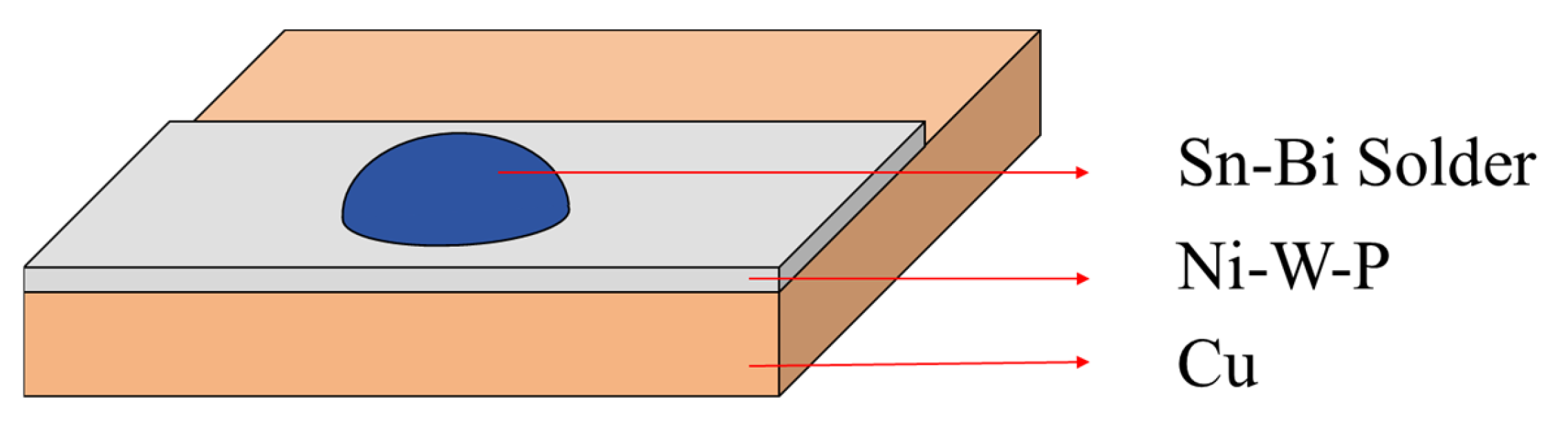
The Interfacial Reaction between Amorphous Ni-W-P Coating and Sn-58Bi Solder

by
Chenyu Li
,
Xiaolin Su
,
Zhongxu Zhang
,
Haitao Ma
*,
Jinye Yao
,
Haohao Xia
and
Yuanbang Zhao
School of Materials Science and Engineering, Dalian University of Technology, Dalian 116024, China
*
Author to whom correspondence should be addressed.
Metals 2024, 14(10), 1107; https://doi.org/10.3390/met14101107
Submission received: 9 August 2024 / Revised: 19 September 2024 / Accepted: 24 September 2024 / Published: 26 September 2024

Abstract

:
With the rapid development of the advanced electronic packaging field, the requirements for the connection between solder and Cu substrate are becoming increasingly stringent. Currently, the commonly used Ni-P diffusion barrier layer in the industry lacks long-term reliability, and its resistivity is higher than that of other substrates. This paper introduces the highly conductive metal element W to modify the binary Ni-P coating and prepares a ternary Ni-W-P coating through electrodeposition to improve this situation. The key parameters for the electrodeposition of ternary Ni-W-P are determined. The isothermal aging reaction of Ni-W-P with Sn-Bi solder at 100 °C was studied, and the results showed that, compared to the conventional Ni-P coating, the Ni-W-P barrier coating with higher W content has a much longer lifespan as a barrier layer and exhibits significantly better electrical conductivity. Additionally, the reaction mechanism between Ni-W-P and the Sn-Bi solder is proposed. This research presents a promising advancement in the development of barrier layers for electronic packaging, potentially leading to more reliable and efficient electronic devices. Introducing tungsten into the Ni-P matrix not only extends the lifespan of the coating but also enhances its electrical performance, making it a valuable innovation for applications requiring high conductivity and durability. This study could guide further investigations into the application of ternary coatings in various electronic components, paving the way for improved designs and materials in the semiconductor industry.

1. Introduction

With the rapid development of advanced electronic packaging, the demand for high-performance and miniaturized electronic devices grows, putting more strain on the solder interconnections between Cu substrates and Sn-based solders. Sn-Ag-Cu (SAC) solders are commonly employed in electronic systems; however, they do present some obstacles, such as a relatively high melting temperature of 217–220 °C and potential reliability issues caused by the creation of brittle intermetallic compounds [1]. Many lead-free solder alloys (such as Sn-Bi, Sn-Ag, and Sn-Zn) are considered viable lead-free substitutes for traditional Sn-Pb alloys. Compared to typical Sn-Pb alloys, these alloys have lower melting temperatures and better wettability [2,3,4]. With the development of miniaturized solder joint sizes, higher demands are placed on both the joints and the solder [5,6]. As the dimensions of the solder joints diminish, the electric, thermal, and mechanical forces exerted on the solder joints increase, rather than decrease, and the reliability of the solder joints faces significant challenges [7,8]. Furthermore, the solder joint interface element interaction, diffusion enhancement, and electromigration are intensified by multiple effects including those of the solder joint soldering reflow process of the intermetallic compound (IMC) grain size [9]. This also places higher demands on the solder and substrate.
The Si chip and substrate thermal expansion mismatch rises with increasing modularity and scalability of electronic components. The electrical components thermally deform more at higher soldering temperatures, which results in more frequent failures. Moreover, at higher temperatures, flaws such as delamination or popcorning failures worsen in packaging that is susceptible to moisture [10]. There is an increasing need to investigate low-melting-point solders, including Sn-Bi or Sn-In alloys, to address these problems [11]. Sn-Bi solder is more affordable and provides superior thermal reliability than Sn-In solder because of its comparatively higher melting temperature.
Sn-Bi solder is a lead-free alloy with a eutectic composition of 42% Sn and 58% Bi (by weight), with a low melting point of 139 °C. As a result, it works well for temperature-sensitive components, flexible electronic components, and low-temperature soldering applications [12,13]. Eutectic Sn-Bi has low viscosity, strong electrical conductivity, low toxicity, and good wettability. Nonetheless, there are issues with eutectic Sn-Bi alloy that need to be resolved through more study and development. For example, its low tensile strength and high brittleness are poor mechanical attributes that reduce its dependability and durability. Additionally, during heat cycling, it is impacted by phase separation and microstructure coarsening, which can compromise its stability and performance [14,15].
There are some issues with the dependability of the bond between the Sn-Bi solder and the Cu substrate. This is mainly because direct bonding between the two leads to the development of brittle Cu-Sn intermetallic compounds (IMCs). The Ni element can be employed as a diffusion barrier layer to slow down the growth of IMCs and produce a good interfacial bond since it reacts with solder more slowly than other elements. The diffusion rate of Ni and Sn is significantly lower than that of Cu and Sn, as was found by Mo et al. [16]. Cu atoms are swapped out for Ni atoms during the creation of (Cu, Ni)6Sn5, which slows down the quick diffusion of Cu atoms in the molten solder. Research by Okamoto et al. showed that when Ni metallization reacts with Sn-Bi eutectic solder, only Ni3Sn4 forms at the interface. Even after 3600 h of solid-state annealing at 135 °C, no other phases were observed, indicating the slow growth kinetics typical of Ni-Sn IMCs [17].
Currently, a common practice is to pre-deposit a Ni-P coating on the Cu substrate [18,19,20]. However, Ni-P coatings also have drawbacks, such as insufficient stability and poor electrical conductivity. To enhance the reliability and improve the conductivity of the Ni-P coating, a third element, W, which has excellent electrical conductivity, is introduced into the Ni-P coating. W has a larger atomic size and does not react with Ni or P to form IMCs, but exists in the coating as a solid solution. The presence of W can effectively pin grain boundaries and hinder the formation of columnar Ni3P grains [21,22].
Neither W nor P can be deposited alone from the solution, but they can co-deposit with the iron-group metal Ni, a process known as induced co-deposition [23,24]. The electroplating cathodic reaction is as follows:
Ni = Ni2+ + 2e
Ni2+ + 2H2O = NiO + 2H+
P + 4H2O = PO43− + 8H+ + 5e
2PO43− + 3Ni2+ = Ni3(PO4)2
W + 4H2O = WO3 + 6H+ + 6e
The concentration of the primary salt in the plating solution directly determines the contents of Ni, W, and P, which also directly affects whether the coating is crystalline or amorphous [25,26,27]. When the W and P content in the coating exceeds a certain critical value, the coating transitions from a crystalline to an amorphous state. In the packaging field, amorphous diffusion barrier layers are far superior to crystalline ones. Amorphous coatings lack grain boundaries that act as fast diffusion paths, significantly reducing the migration speed of Cu into the solder and thereby suppressing the growth of Cu-Sn IMCs, achieving the effect of a diffusion barrier.
Based on this foundation, this study developed a ternary Ni-W-P diffusion barrier layer (with a P content of 21–23 wt.% and a W content of 7–8 wt.%) using pulse electroplating by adjusting additives, primary salt concentration, and electroplating parameters. The coating is uniform and dense, has good electrical conductivity, and exhibits high thermal stability. The coating was subjected to isothermal aging and multiple reflow tests with Sn-Bi solder, and the diffusion barrier rate of the Ni-W-P layer was evaluated, proposing an interface reaction mechanism.

2. Materials and Methods

Copper substrates measuring 10 mm × 20 mm × 1.5 mm were selected for this experiment. The preparation of these substrates involved a meticulous sequential polishing process. Initially, the copper plates were ground with 400#, 1500#, and 2000# SiC sandpaper, progressively refining the surface. This was followed by further polishing using diamond suspensions with particle sizes of 1.5 μm and 0.5 μm to achieve an even smoother finish. Each step in the polishing process was designed to create a progressively smoother surface. After polishing, the copper plates underwent ultrasonic cleaning in ethanol for approximately 30 s, effectively removing any remaining particles or contaminants from the surface. To ensure the complete removal of residues, the copper plates were thoroughly rinsed with deionized water before each step. Finally, the plates were dried using cold air. This carefully controlled process ensured that the copper substrates were optimally prepared for subsequent experiments.
The composition of the electroplated Ni-W-P bath is shown in Table 1. The Ni-W-P plating solution, NiSO4 NaH2PO4, and Na2WO4 were used as the main salts and as the sources of Ni, W, and P in the plating layer; sodium citrate was used as the complexing agent; H3BO3 was used as the stabilizing agent; sodium saccharin was used as the leveling agent; and SDS was used as the surfactant.
To produce a smooth and dense coating while minimizing the impact of concentration polarization on coating quality, pulse electroplating was utilized. The specific process parameters were current density 5 A/dm2, frequency 1000 Hz, duty cycle 50%, and operating time 1200 s.
The thickness of the deposited layer was measured using a metallurgical microscope. The composition of the Ni-W-P coating was analyzed using Scanning Electron Microscopy (SEM) and Energy-Dispersive Spectroscopy (EDS). The SEM is made by Zeiss Group (Shanghai, China), and the EDS is made by Oxford Instruments (Shanghai, China). Additionally, X-ray Diffraction (XRD) analysis was performed to determine the crystalline structure of the Ni-W-P coating. The XRD analysis employed a Cu target with a Ni filter operating at 40 kV and 40 mA, with a scan step size of 0.05° and a duration of 0.5 s per step. This approach effectively characterizes the crystal structure within the coating.
During the soldering process, rosin flux was evenly applied to the copper substrate, and Sn-58Bi solder balls with a diameter of 200 μm were used to form Sn-58Bi/Ni-W-P solder joints. The soldering process took place in a reflow oven at 180 °C. All samples use the same heater, which is programmable for brazing. The sample heating time was uniform at 58 s, with holding times of 60 s, 180 s, and 300 s. Based on these conditions, 180 s was selected as the optimal reflow soldering time, and subsequent isothermal aging experiments were conducted in an oil bath at 100 °C.
The schematic diagram of the soldering process is shown in Figure 1.
SEM and EDS were employed to investigate the intermetallic compounds (IMCs) formed between the two coatings and the pure tin solder. Before SEM characterization of the solder joint cross-sections, the samples were ground with SiC sandpaper and then polished using diamond paste with particle sizes of 1.5 μm and 0.5 μm. A chemical etching process was performed using a weak acid solution consisting of 93% C2H5OH, 2% HNO3, and 5% HCl, all in volumetric proportions, to reveal the microstructure. The samples were chemically etched for surface morphology characterization using a solution containing 90% ethanol and 10% nitric acid by volume.

3. Results and Discussion

3.1. Effect of Main Salt Concentration on Coating Composition

In this study, preliminary experimental exploration determined the concentration range of the primary salts and the electroplating process parameters. Using a W:P ratio of 1:1 as a baseline, the effects of high W/low P and low W/high P ratios on the coating and the interface reactions at the solder joints were investigated. This provided direction for further exploration of the W and P content or ratios that might result in a more pronounced diffusion barrier effect. While keeping the concentration of Na2WO4·2H2O constant at 0.1 mol/L in the plating solution, the concentration of NaH2PO2·H2O was varied to prepare Ni-W-P diffusion barrier layers with W:P molar ratios of 1:2, 1:1, and 2:1. Table 2 shows the elemental composition of the coatings prepared with different NaH2PO2·H2O concentrations.
It can be seen that, with the increase in the W:P molar ratio in the plating solution, the content of P gradually decreased and the content of W gradually increased, while Ni maintained a very high proportion and was still the base element of the coating. Notably, there was a significant change in W content when the ratio shifted from W:P = 1:2 to 1:1. By comparing the effects of different primary salt concentrations in the plating solution (molar ratios W:P = 1:2, 1:1, 2:1) on the chemical composition and thickness of the coating, it was found that within the range of primary salt concentrations controlled in this experiment, as the W:P ratio increased (with a decrease in P concentration), the thickness of the coating gradually decreased. The P content in the coating decreased while the W content increased, with a significant change observed when the ratio shifted from W:P = 1:2 to 1:1 (from 0.32% to 2%). However, the change in coating composition did not exactly follow the trend of the W:P ratio set in the plating solution, indicating a competitive relationship between W and P deposition during co-deposition. This finding provides a valuable reference for adjusting the coating composition in future studies.

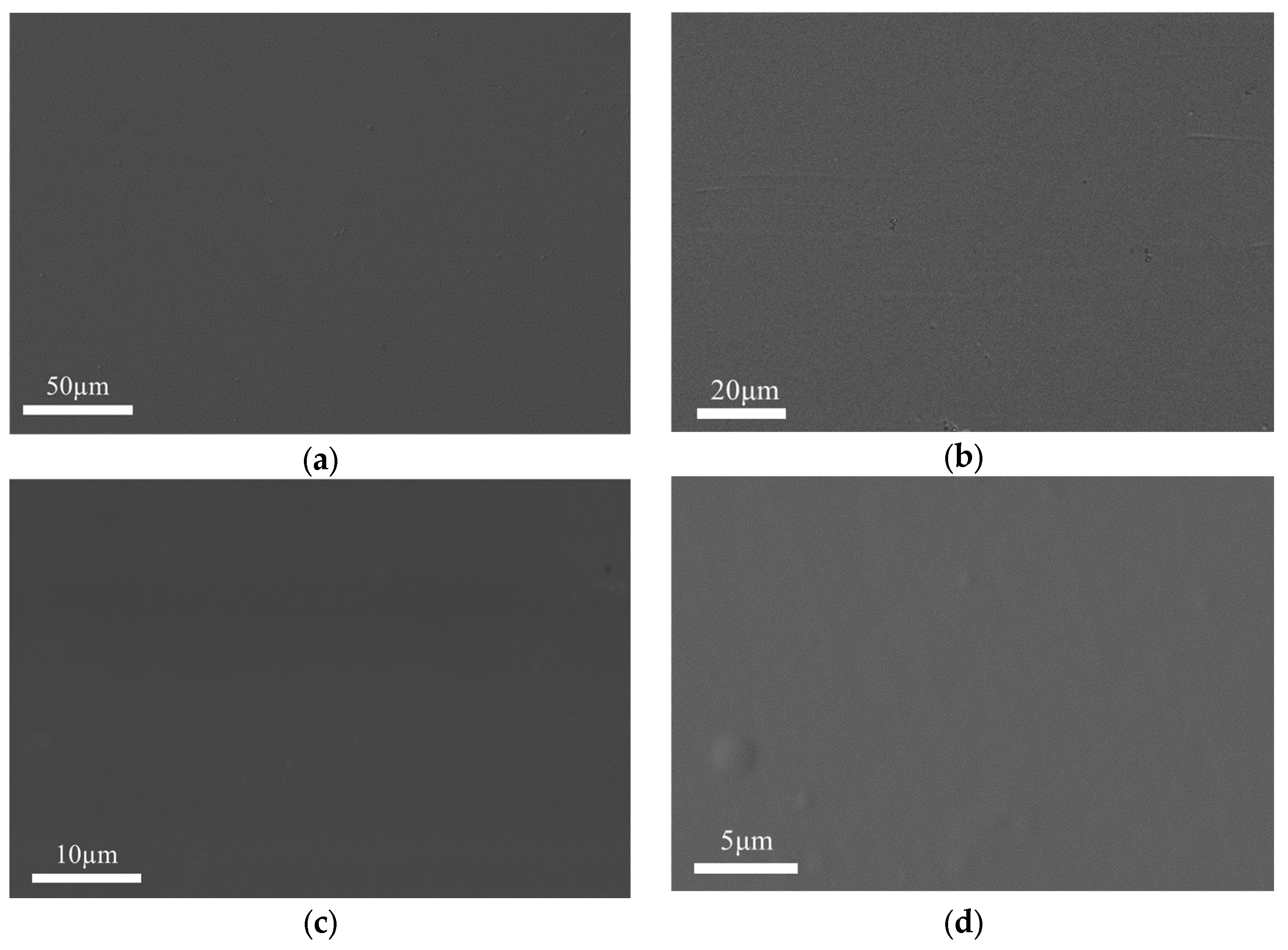
3.2. Surface Topography and Crystal Structure of the Coating

Building on previous work, a dense and smooth ternary Ni-W-P diffusion barrier layer was prepared with a primary salt concentration corresponding to a W:P ratio of 1:1. The coating exhibited a P content of 21–23 wt.% and a W content of 7–8 wt.%. Macroscopically, the surface of the coating appeared smooth and flat, and had a bright silver color. Microscopically, the surface of the coating was observed at magnifications of 1000×, 2000×, 5000×, and 10,000× using Scanning Electron Microscopy (SEM), as shown in Figure 2a–d. The coating surface was uniform and highly flat, with no significant defects, making it well-suited for use as a diffusion barrier layer. These images with different magnifications are put together to show that the coating maintained a high degree of flatness over a wide range and at high magnifications, which reduced experimental errors, and this facilitates the next step in brazing experiments.
In addition to analyzing the surface morphology of the coating, X-ray Diffraction (XRD) analysis was performed to determine the crystalline structure of the Ni-W-P coating. The results are shown in Figure 3. The distinct characteristic diffraction peaks of the Cu substrate were observed at 43.37°, 50.49°, and 74.13°. Around the characteristic diffraction peak of Ni at 44.5°, significant peak broadening was observed, indicating that the crystalline structure of the coating was amorphous. This amorphous structure reduced the density of grain boundaries, thereby decreasing the diffusion pathways for Cu atoms. As a result, the likelihood of forming brittle Cu-Sn intermetallic compounds (IMCs) was reduced, enhancing the mechanical reliability of the joint.

3.3. Electrical Conductivity and Wettability

In the field of advanced electronic packaging, the conductive performance of electronic devices is crucial. The resistivity of Ni is moderate among metal conductors (7.8 × 10⁻⁸ Ω·m) [28]. However, the addition of the semiconductor element P in the Under Ball Metal (UBM) layer further reduced the conductivity. Introducing a new element with high conductivity is a promising approach to address this issue. The metal element W has a low resistivity (1.82 × 10⁻⁹ Ω·m) and a significantly different atomic size compared to Ni and P [29]. The atomic size of W is much higher than that of Ni and P, and according to the phase diagrams of Ni, W, and P and the temperature at which they were deposited, W does not react with Ni and P and does not form an intermetallic compound, whereas the presence of W was detected by EDS spectroscopy, and the combination of the above conditions suggests that W can only be solidly dissolved into the original Ni-P coatings in the form of atoms. W can only be solidly dissolved into the original Ni-P coating in the form of atoms. W is like a separate phase, as the overall conductivity of the coating is improved. Table 3 also proves this point. Moreover, the presence of W increases the degree of lattice distortion in the coating, enhancing its stability and mechanical properties.
After preliminary experimental preparation, Ni-P and Ni-W-P coatings were prepared on copper samples of the same size. Considering that both are thin-film substrates, a four-point probe resistance tester was used to measure the sheet resistance of the Ni-P and Ni-W-P coatings to better characterize their electrical conductivity. For each group, three different locations on the same coating were selected for measurement. The results are shown in Table 3. It can be seen that the average sheet resistance of the Ni-W-P coating was 0.534 mΩ/sq, while that of the Ni-P coating was 0.616 mΩ/sq. This indicates that the electrical conductivity of the Ni-W-P coating was superior to that of the Ni-P coating. The introduction of the highly conductive metal element W not only maintained the amorphous structure of the coating, but also enhanced the electrical efficiency of the UBM layer.
To evaluate the solderability of the Ni-W-P coating, the contact angle of the solder joints was measured using a contact angle meter after soldering. In this study, Sn-Bi solder was used at a soldering temperature of 180 °C, with three different soldering times selected: 1 s, 60 s, and 300 s, respectively, for soldering on Ni-P- and Ni-W-P-coated substrates. Two Sn-Bi solder balls were soldered onto each sample, and the wetting angle of the solder joints was measured. The wetting angle data were processed using Trim Mean, and the summarized results are shown in Table 4. The wetting angles of Sn-Bi/Ni-W-P solder joints at different times were significantly smaller than those of Sn-Bi/Ni-P solder joints. These results indicate that the presence of W effectively improved the wettability of the Sn-Bi solder, thereby enhancing the soldering performance compared to the Ni-P substrate.

3.4. Interface Reactions

Three different compositions of Ni-W-P diffusion barrier layers were obtained through preliminary preparation. The thicknesses of the coatings prepared under the same conditions are shown in Table 5.
To investigate the interface reactions after soldering and the growth patterns of IMCs, reflow soldering was carried out at 180 °C for 60 s, 180 s, and 300 s, respectively. This was intended to explore the relationship between the diffusion barrier effect of the Ni-W-P coating and its composition. Additionally, one of the coating compositions was selected for multiple reflow soldering processes, followed by isothermal aging at 100 °C, to study the growth pattern of IMCs after reflow soldering and the consumption rate of the diffusion barrier layer.
Since the coating was not completely consumed within the set soldering time, EDS (Energy-Dispersive Spectroscopy) analysis of the interface showed that the metal composition and content of the IMCs were similar. Based on the composition content, these IMCs were identified as (Ni, Cu)3Sn4, indicating that the IMC formation mechanism was consistent.
Based on Figure 4 and Figure 5, and Table 5, the effectiveness of the coating as a diffusion barrier for Cu can be inferred from the thickness and composition of the barrier layer. The influence of thickness on the diffusion barrier effect is evident—the thicker the coating, the stronger its ability to block diffusion. If only the diffusion barrier effect is considered, theoretically, the thicker the coating, the better. However, in practical engineering applications, trends and requirements lean towards lightweight and miniaturized integration, necessitating further study of other conditions of the coating to improve the diffusion barrier effect. The following discussion will explore the effectiveness of the Ni-W-P layer as a diffusion barrier based on the morphology, composition, thickness, and growth rate of the IMC layer at the soldering interface. The blocking mechanism of the diffusion barrier layer will also be studied.

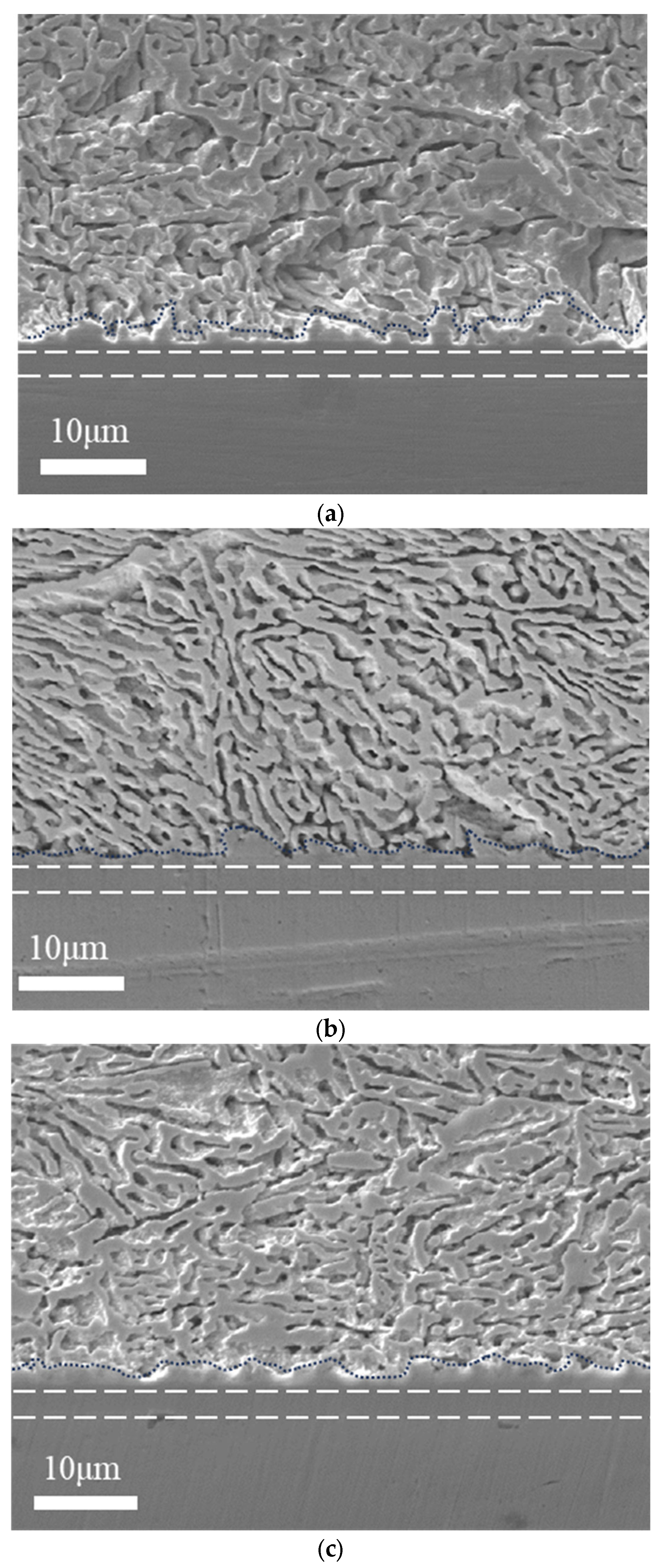
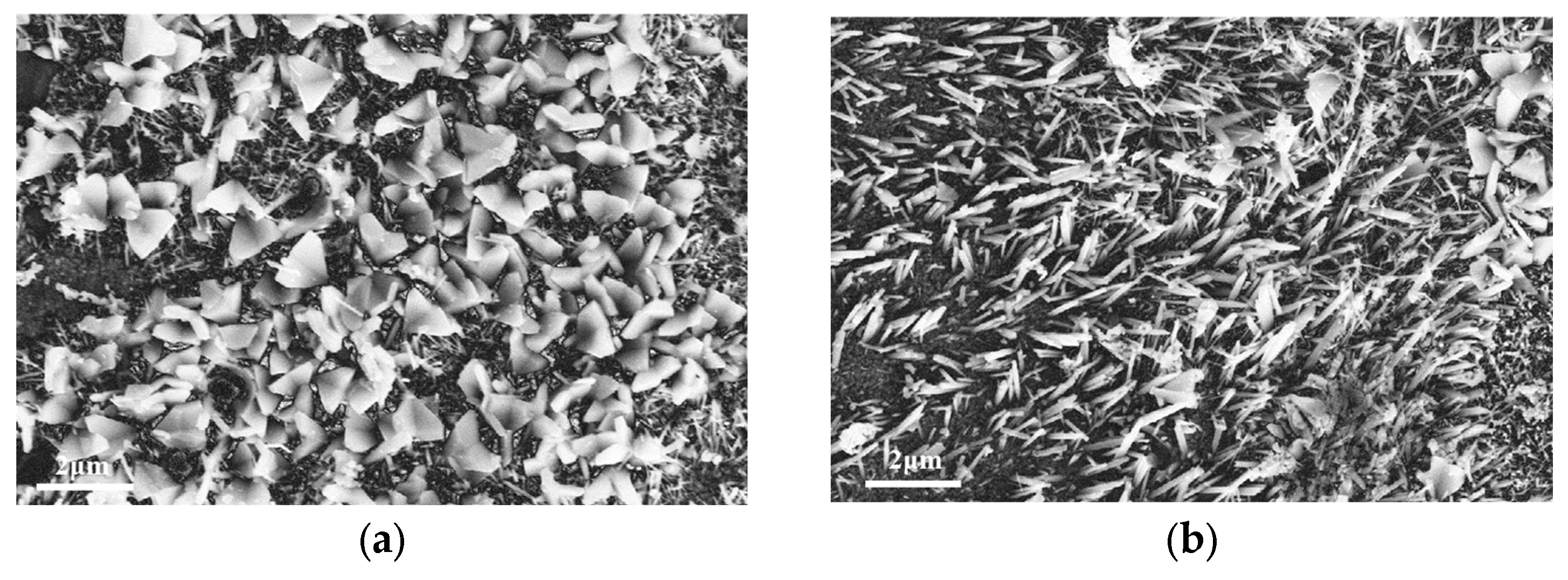
3.4.1. IMC Layer Growth Morphology and Composition

After treating the solder joints with corrosion following reflow soldering, the IMC top-view images were observed using a field emission scanning electron microscope (FE-SEM) at 20,000× magnification. As shown in Figure 6, two shapes were observed:
Utilizing the Ni-Sn-Cu ternary phase diagram, it was deduced that the predominant IMC was (Ni, Cu)3Sn4. The IMC at the interface exhibited several different morphologies: one was the standard dart-like (Ni, Cu)3Sn4; another was a blocky compound, which matched the morphology observed in the cross-section; and the last one was a needle-like compound. The atomic ratio of (Ni, Cu) to Sn is 2.93:4.01, which is approximately 3:4. This elemental ratio closely aligns with that of (Ni, Cu)3Sn4. It can be concluded that the IMC layer thickness increases with longer soldering times. Analysis of the SEM microstructure images of the solder joint cross-sections suggests that IMCs with different morphologies have varying energies due to differences in Ni and Cu content in the compounds, and the formation of IMCs follows the principle of energy minimization. (Ni, Cu)3Sn4 forms at the Ni-W-P/Sn interface, and its morphology changes significantly with increased reflow time. For example, as reflow time increases, the IMC at the interface grows significantly, with the appearance of blocky IMCs along with dart-like, blocky, and needle-like (Ni, Cu)3Sn4. It can be inferred that dart-like (Ni, Cu)3Sn4 is more likely to form during short-term soldering experiments. As the soldering time extends, the Cu content in (Ni, Cu)3Sn4 gradually increases, making needle-like (Ni, Cu)3Sn4 more likely to appear. This can be attributed to the varying stability of different (Ni, Cu)3Sn4 morphologies depending on the Ni and Cu content.

3.4.2. IMC Layer Thickness

Due to the IMC’s dart-like, blocky, and needle-like morphologies, two methods were used to calculate the thicknesses of the blocky and needle-like IMC layers based on image analysis. For the dart-like and blocky IMCs, the cross-sectional area (A) and linear length (L) of the IMC layer in the SEM image of the Sn-58Bi/Ni-W-P/Cu interface were measured. The average thickness (X) of the IMC layer was determined by dividing the cross-sectional area (A) by the linear length (L), as shown in the following formula:
X = A L
A comparison between the microstructures and measured thicknesses of the IMC layers at the interface under the same soldering time but different W and P molar ratios is shown in Table 6.
It was found that at a soldering time of 60 s, the IMC thickness for W:P = 1:2 < W:P = 1:1 < W:P = 2:1; at 180 s, the IMC thickness for W:P = 2:1 < W:P = 1:1 < W:P = 1:2; and at 300 s, the IMC thickness for W:P = 2:1 < W:P = 1:2 < W:P = 1:1. Although no specific pattern was observed in the IMC layer thickness under different W and P molar ratios for the same soldering time, the differences in IMC layer thickness among the three different coatings were not significant. The initial thickness of the IMC is related to the coating thickness. This was found by analysing coatings prepared with different molar ratios.

3.4.3. Interface Reaction Rate

Using Origin 2018 software, the data from Table 6 were plotted to obtain the curve of reflow time versus IMC thickness, as shown in Figure 7. From the curve of IMC thickness versus reflow time under different chemical ratios, it can be seen that as the reflow time increased, the growth rate of the IMC thickness gradually slowed down.
We will analyze the reasons for this change. The IMC layer grows through atomic diffusion, a process proportional to the square root of time. This means that the initial growth is relatively fast, but as time progresses, the diffusion path lengthens, and the diffusion resistance increases, causing the growth rate to gradually decrease. As the IMC layer thickens, the number of reactive atoms at the interface decreases, and the formed IMC layer may start to act as a barrier to further diffusion, creating a so-called “diffusion barrier”.
By comparing the microstructure of the IMC layer at different soldering times and under the same W and P molar ratio, it was observed that the IMC layer thickened significantly at a soldering time of 60 s. However, at 180 s and 300 s, the IMC layer did not appear as thick as at 60 s. This phenomenon can be analyzed as follows: within 300 s of reflow time and without aging treatment, the interfacial IMC composition is consistently (Ni, Cu)3Sn4, but (Ni, Cu)3Sn4 exhibits different shapes, including dart-like, blocky, and needle-like shapes, leading to different appearances.
During short-term soldering, the growth rate of the IMC is significantly influenced by thickness: the thicker the diffusion barrier layer, the thinner the IMC layer. However, with extended soldering time, the composition of the diffusion barrier layer becomes more influential, particularly the effect of W content. As the W content increases, the growth rate of the IMC layer slows down. Increasing the W and P content within the barrier layer may help form a thinner IMC layer because the addition of W and P may affect the kinetic processes of interfacial reactions, and as the W content increases and P content decreases, the diffusion barrier effect strengthens. Notably, Cu primarily uses grain boundaries as diffusion pathways. The Ni-W-P coating is in an amorphous state with very low grain boundary density, which blocks the diffusion of Cu. Regarding the reaction between Ni and Sn-Bi solder, the presence of W and P atoms reduces the contact between Ni and Sn by occupying Ni sites, and the large W atoms hinder IMC formation, thereby slowing down its growth rate and inhibiting the growth of the IMC layer.
As for the Ni-W-P coating itself, since the size of W atoms is much larger than that of Ni and P, it is speculated that during the isothermal aging process, W does not participate in the formation of new compounds, but instead plays a role in pinning grain boundaries, increasing the degree of lattice distortion. This results in a higher energy requirement for the formation of (Ni, Sn)3P, making its transformation very slow and achieving long-term stability.

3.4.4. Isothermal Aging Treatment

An isothermal aging treatment was conducted at 100 °C for 240 h, and surface composition analysis was performed using an EDS spectrometer. The results, as shown in the following figure, indicate that the P element accumulated at the interface, and Sn began to diffuse into the coating. Based on the Ni-P and Ni-Sn phase diagrams, it was inferred that some Ni3P started to form at the interface. Through reactions during soldering and diffusion during aging, Ni from the coating transferred into the solder, with Sn in the solder substituting for Ni, forming (Ni, Sn)3P. Under these conditions, (Ni, Sn)3P typically forms vertical columnar crystals whose grain boundaries can act as fast diffusion channels, failing to achieve a diffusion barrier effect. Therefore, if aging time continues to increase, the Ni-W-P coating will continue to transform into (Ni, Sn)3P. However, the presence of W inhibits the transformation rate of (Ni, Sn)3P. As shown in Figure 8 and Figure 9, after 240 h of isothermal aging at 100 °C, only a thickness of 0.395 μm could be observed under a scanning electron microscope, fully demonstrating the stability of this barrier layer and its capability to serve in high-temperature environments for extended periods.
By comparing the IMC layer thickness of Sn-58Bi/Ni-W-P coatings of the same composition/Cu at different soldering times, it can be concluded that the IMC layer thickness increases with longer soldering times. Analyzing the SEM microstructure images of the solder joint cross-sections suggests that IMCs with different morphologies have different energies based on the Ni and Cu content in the compounds. (Ni, Cu)3Sn4 forms at the Ni-W-P/Sn interface, and its morphology changes significantly with increasing reflow time. For example, with longer reflow times, the IMC at the interface grows significantly, forming blocky IMCs.

4. Conclusions

This study employed a constant current pulse electroplating method, adjusting the conditions for preparing the Ni-W-P coating to obtain electroplating parameters that yield a coating with good surface quality. By comparing Cu/Ni-W-P substrates with different compositions of Ni-W-P coatings soldered with Sn-58Bi at different times, the relationship between the growth of the intermetallic compound (IMC) layer at the interface and the coating composition, thickness, and soldering time was established. Based on the research on the preparation of Ni-W-P coatings and the soldering process, the following conclusions were drawn:
(1)
By adjusting the concentration of additives and the electroplating process parameters, a coating with excellent surface quality can be obtained, and under these conditions, the thickness of the coating after 20 min of pulse electroplating is approximately 3 to 4 μm.
(2)
During the co-deposition process of electroplating, tungsten (W) and phosphorus (P) exhibit a competitive relationship, and the content of W and P does not have a linear correlation with the ratio of the main salt concentration in the plating solution.
(3)
The plating is amorphous, the addition of W to the Ni-P plating improves the electrical conductivity of the plating, and its square resistance decreases from 0.616 mΩ/sq to 0.534 mΩ/sq.
(4)
The growth rate of the IMC layer at the interface is very fast when the welding time is from 60 s to 180 s. However, the growth rate of the IMC layer is greatly reduced after increasing the welding time, which shows the excellent barrier effect of the Ni-W-P coating.
(5)
For Ni-W-P coatings with the same welding time, the higher the W content, the slower the growth rate of the IMCs layer at the interface.
(6)
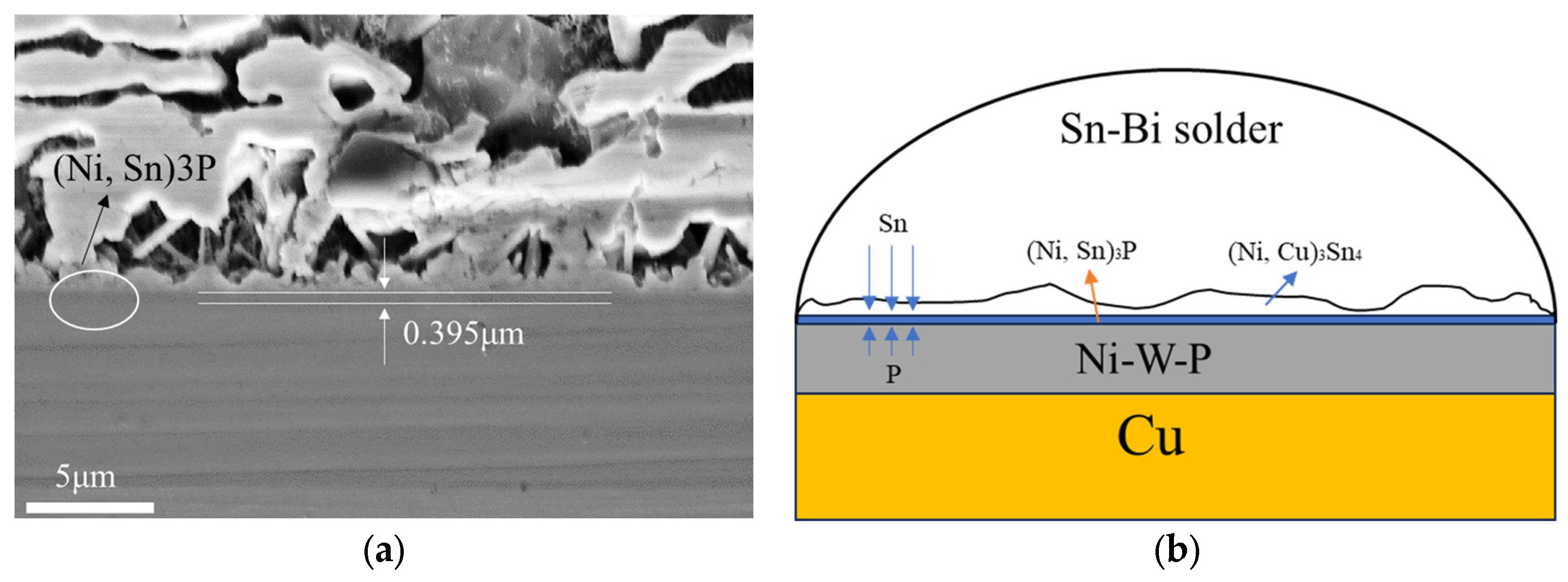
The Ni-W-P coating effectively prevents the diffusion of copper (Cu) atoms, and after isothermal aging at 100 °C for 240 h, the Ni-W-P coating is transformed into only 0.395 μm, which is less than one-tenth of the total thickness of the coating, and it has good thermal stability.
(7)
The Ni-W-P coating will gradually transform into (Ni, Sn)3P, which may eventually lead to its failure.

Author Contributions

Software, Z.Z.; Validation, C.L. and J.Y.; Investigation, C.L., H.X. and Y.Z.; Data curation, C.L. and X.S.; Writing—original draft, C.L.; Writing—review & editing, H.M. All authors have read and agreed to the published version of the manuscript.

Funding

This research received no external funding.

Data Availability Statement

The original contributions presented in the study are included in the article, further inquiries can be directed to the corresponding author.

Conflicts of Interest

The authors declare no conflict of interest.

References

  1. Abtew, M.; Selvaduray, G. Lead-free Solders in Microelectronics. Mater. Sci. Eng. R Rep. 2000, 27, 95–141. [Google Scholar] [CrossRef]
  2. Islam, R.A.; Chan, Y.C.; Jillek, W.; Islam, S. Comparative study of wetting behavior and mechanical properties (microhardness) of Sn–Zn and Sn–Pb solders. Microelectron. J. 2006, 37, 705–713. [Google Scholar] [CrossRef]
  3. Wang, M.; Wang, J.; Feng, H.; Ke, W. Effect of Ag3Sn intermetallic compounds on corrosion of Sn-3.0Ag-0.5Cu solder under high-temperature and high-humidity condition. Corros. Sci. 2012, 63, 20–28. [Google Scholar] [CrossRef]
  4. Wei, C.; Liu, Y.C.; Han, Y.J.; Wan, J.B.; Yang, K. Microstructures of eutectic Sn–Ag–Zn solder solidified with different cooling rates. J. Alloys Compd. 2008, 464, 301–305. [Google Scholar] [CrossRef]
  5. Dele-Afolabi, T.T.; Ansari, M.; Hanim, M.A.; Oyekanmi, A.A.; Ojo-Kupoluyi, O.J.; Atiqah, A. Recent advances in Sn-based lead-free solder interconnects for microelectronics packaging: Materials and technologies. J. Mater. Res. Technol. 2023, 25, 4231–4263. [Google Scholar] [CrossRef]
  6. Lau, J.H. Recent advances and trends in advanced packaging. IEEE Trans. Compon. Packag. Manuf. Technol. 2022, 12, 228–252. [Google Scholar] [CrossRef]
  7. Li, Y.; Fu, G.; Wan, B.; Wu, Z.; Yan, X.; Zhang, W. A study on the effects of electrical and thermal stresses on void formation and migration lifetime of Sn3.0Ag0.5Cu solder joints. Solder. Surf. Mt. Technol. 2022, 34, 162–173. [Google Scholar] [CrossRef]
  8. Li, Y.; Fu, G.; Wan, B.; Yan, X.; Zhang, W.; Li, W. Phase-field modeling of lead-free solder joint void growth under thermal-electrical coupled stress. J. Electron. Mater. 2022, 51, 259–272. [Google Scholar] [CrossRef]
  9. Zhang, Z.; Chen, J.; Wang, J.; Han, Y.; Yu, Z.; Wang, Q.; Zhang, P.; Yang, S. Effects of solder thickness on interface behavior and nanoindentation characteristics in Cu/Sn/Cu microbumps. Weld. World 2022, 66, 973–983. [Google Scholar] [CrossRef]
  10. McCluskey, P.; Munamarty, R.; Pecht, M. Popcorning in PBGA Packages During IR Reflow Soldering. Microelectron. Int. 1997, 14, 20–23. [Google Scholar] [CrossRef]
  11. Singh, A.; Durairaj, R. Study on Hardness and Shear Strength with Microstructure Properties of Sn52Bi/Cu + 1% Al2O3 Nanoparticles. IOP Conf. Ser. Mater. Sci. Eng. 2020, 834, 012075. [Google Scholar] [CrossRef]
  12. Hua, F.; Mei, Z.; Glazer, J. In Eutectic Sn–Bi as an Alternative to Pb-Free Solders. In Proceedings of the 48th Electronic Components and Technology Conference, Seattle, WA, USA, 25–28 May 1998. [Google Scholar]
  13. Mei, Z.; Morris, J.W. Characterization of eutectic Sn–Bi solder joints. J. Electron. Mater 1992, 21, 599–607. [Google Scholar] [CrossRef]
  14. Liu, P.L.; Shang, J.K. Interfacial embrittlement by bismuth segregation copper/tin–bismuth Pb-free solder interconnect. J. Mater. Res. 2001, 16, 1651–1659. [Google Scholar] [CrossRef]
  15. Zou, H.F.; Zhang, Q.K.; Zhang, Z.F. Transition of Bi embrittlement of SnBi/Cu joint couples with reflow temperature. J. Mater. Res. 2010, 26, 449–454. [Google Scholar] [CrossRef]
  16. Mo, C.C.; Tran, D.P.; Juang, J.Y.; Chen, C. Effect of Intermetallic Compound Bridging on the Cracking Resistance of Sn2.3Ag Microbumps with Different UBM Structures under Thermal Cyclin. Metals 2021, 11, 1065. [Google Scholar] [CrossRef]
  17. Okamoto, H. Ni-Zn (nickel-zinc). J. Phase Equilibria 2003, 24, 280–281. [Google Scholar] [CrossRef]
  18. Alam, M.O.; Chan, Y.C.; Tu, K.N. Correlation between chemical reaction and brittle fracture found in electroless Ni(P)/immersion gold–solder interconnection. J. Appl. Phys. 2003, 94, 4108. [Google Scholar] [CrossRef]
  19. Zeng, K.; Vuorinen, V.; Kivilahti, J.K. Interfacial reactions between lead-free SnAgCu solder and Ni(P) surface finish on printed circuit boards. IEEE Trans. Electron. Packag. Manuf. 2002, 25, 162–167. [Google Scholar] [CrossRef]
  20. Chin, Y.T.; Lam, P.K.; Yow, H.K.; Tou, T.Y. Transmission electron microscopy studies of interfacial reactions and void formation in lead-free solders with minor elements. J. Mater. 2010, 25, 1304–1311. [Google Scholar] [CrossRef]
  21. Yang, Y.; Balaraju, J.N.; Chong, S.C.; Xu, H.; Liu, C.; Silberschmidt, V.V.; Chen, Z. Significantly retarded interfacial reaction between an electroless Ni-W-P metallization and lead-free Sn-3.5Ag solder. J. Alloys Compd. 2013, 565, 11–16. [Google Scholar] [CrossRef]
  22. Bae, S.H.; Nguyen, Y.N.; Son, I. Ni-W-P layer-induced strength improvement of solder joint in Bi2Te3 thermoelectric module. Sci. Technol. Weld 2023, 28, 399–406. [Google Scholar] [CrossRef]
  23. Brenner, A. Electrodeposition of Alloys; Academic Press Inc.: New York, NY, USA, 1963; pp. 160–165. [Google Scholar]
  24. Lin, C.S.; Lee, C.Y.; Chen, F.J.; Li, W.C. Structural Evolution and Internal Stress of Nickel-Phosphorus Electrodeposits. Electrochem. Soc. 2005, 152, C370–C375. [Google Scholar] [CrossRef]
  25. Lai, G.-Q.; Liu, H. Electrodeposition of functionally graded Ni-W/Er2O3 rare earth nanoparticle composite film. Int. J. Miner. Metall. Mater. 2020, 27, 818–829. [Google Scholar] [CrossRef]
  26. Alam, M.O.; Chan, Y.C.; Hung, K.C. Preparation and wear resistance of electrodeposited Ni–W/diamond composite coatings. Microelectron. Reliab. 2002, 4, 1065. [Google Scholar] [CrossRef]
  27. Zhan, X.; Zhang, P.; Voyles, P.M.; Liu, X. Effect of tungsten alloying on short-to-medium-range-order evolution and crystallization behavior of near-eutectic amorphous Ni–P. Acta Mater. 2017, 122, 400–441. [Google Scholar] [CrossRef]
  28. Farrell, T.; Greig, D. The electrical resistivity of nickel and its alloys. J. Phys. C Solid State Phys. 1968, 1, 1359. [Google Scholar] [CrossRef]
  29. Petroff, P.; Sheng, T.T.; Sinha, A.K.; Rozgonyi, G.A.; Alexander, F.B. Microstructure, growth, resistivity, and stresses in thin tungsten films deposited by rf sputtering. J. Appl. Phys. 1973, 44, 2545–2554. [Google Scholar] [CrossRef]
Figure 1. Reflow soldered construction.
Metals 14 01107 g001
Figure 2. Secondary electron SEM images of the surface of Ni-W-P deposits: (a) magnified at 1000×; (b) magnified at 2000×; (c) magnified at 5000×; (d) magnified at 10,000×.
Metals 14 01107 g002
Figure 3. XRD spectra of different compositions of amorphous Ni-W-P deposits.
Metals 14 01107 g003
Figure 4. Scanning electron microscopy (SEM) images of the cross-sections at the solder joint interface after 60 s of reflow soldering with different compositions of coatings. (a) W:P = 1:2; (b) W:P = 1:1; (c) W:P = 2:1.
Metals 14 01107 g004
Figure 5. SEM images of the cross-sections at the solder joint interface with the coating having a W:P molar ratio of 1:1. (a) After 180 s of reflow soldering; (b) after 300 s of reflow soldering.
Metals 14 01107 g005
Figure 6. (a) Dart-like and blocky. (b) Needle-like.
Metals 14 01107 g006
Figure 7. Line graph of reflow time versus IMCs thickness.
Metals 14 01107 g007
Figure 8. Elemental surface distribution after 240 h of aging.
Metals 14 01107 g008
Figure 9. (a) Thickness of (Ni, Sn)3P layer after 240 h of aging; (b) schematic of Sn and P element migration.
Metals 14 01107 g009
Table 1. Composition of Ni-W-P electrolyte.
ElementCompositions (g/L)Information on Chemical Reagents
NiSO4·6H2O40DAMAO, Tianjin, China
NaH2PO2·H2O10–30DAMAO, Tianjin, China
Na2WO4·2H2O33DAMAO, Tianjin, China
C6H5Na3O7·2H2O100DAMAO, Tianjin, China
H3BO320Aladdin, Shanghai, China
C7H4NaO3S7·2H2O6Aladdin, Shanghai, China
CH3(CH2)11OSO3Na0.3Aladdin, Shanghai, China
Table 2. Composition and content of coatings prepared with different primary salt concentrations (atomic%).
ElementW:P = 1:2W:P = 1:1W:P = 2:1
Ni73.31%76.71%74.50%
P26.37%21.29%23.13%
W0.32%2.00%2.37%
Table 3. Sheet resistance of the different plated layer.
Plated LayerNi-PNi-W-P
Sheet Resistance mΩ/sq0.6100.535
0.6200.532
0.6170.534
Average0.6160.534
Table 4. Contact angles of solder balls on different substrates.
Soldering TimeNi-PNi-W-P
1 s46.31°43.60°
60 s43.41°42.43°
300 s44.75°40.84°
Table 5. Thicknesses of diffusion barrier layers prepared with different molar ratios of plating solutions.
CompositionW:P = 1:2W:P = 1:1W:P = 2:1
Plating thickness4.03 μm3.89 μm3.08 μm
Table 6. IMCs layer thickness.
TimeW:P = 1:2W:P = 1:1W:P = 2:1
60 s0.924 μm0.929 μm1.068 μm
180 s1.321 μm1.203 μm1.145 μm
300 s1.371 μm1.374 μm1.267 μm
Disclaimer/Publisher’s Note: The statements, opinions and data contained in all publications are solely those of the individual author(s) and contributor(s) and not of MDPI and/or the editor(s). MDPI and/or the editor(s) disclaim responsibility for any injury to people or property resulting from any ideas, methods, instructions or products referred to in the content.

