Communication

ACOM/TEM and EBSD Microstructure Characterization of ECAE-Processed Zirconium

by
Mychelle Vianna Pereira Companhoni
1,2,3,*,
Além-mar Bernardes Gonçalves
1,
Maurizio Ferrante
4,
Vitor Sordi
4 and
André Luiz Pinto
2,3
1
Physics Institute, Federal University of Mato Grosso do Sul, Campo Grande 79070-900, Brazil
2
Brazilian Center for Physics Research, Rio de Janeiro 22290-180, Brazil
3
Materials Science Department, Military Institute of Engineering, Rio de Janeiro 22290-270, Brazil
4
Materials Science Department, São Carlos Federal University, São Carlos 13565-905, Brazil
*
Author to whom correspondence should be addressed.
Metals 2024, 14(6), 624; https://doi.org/10.3390/met14060624
Submission received: 23 February 2024 / Revised: 3 May 2024 / Accepted: 9 May 2024 / Published: 25 May 2024

Abstract

:
Materials produced through equal channel angular extrusion (ECAE) may offer enhanced mechanical properties over classic thermomechanical processing like extrusion or rolling. Conventional techniques such as electron backscatter diffraction (EBSD) may be insufficient to properly characterize the microstructure of these materials. Darkfield (DF) transmission electron microscopy (TEM), on the other hand, may lead to erroneous conclusions with respect to grain size. In this work, zirconium was submitted to ECAE deformation through four passes in the Bc route at 350 °C. The microstructure was evaluated through FEG-SEM/EBSD (field emission gun–scanning electron microscopy), DF TEM, and ACOM/TEM (automated crystal orientation mapping in TEM). EBSD revealed that the microstructure was heterogeneous with a few large grains surrounded by a fine submicrometric structure, which was only partially resolved through this technique. The fine structure was, however, described through ACOM/TEM. DF TEM was revealed to be somewhat unreliable when the same region was evaluated through ACOM/TEM. Therefore, a combination of techniques seems to be required for proper characterization.

1. Introduction

Severe Plastic Deformation (SPD) has been an emerging technique to produce ultra-fine-grained (UFG) materials with exceptional properties. Nanostructured or nanosized materials can be defined as those with crystalline domains in the range of 1 to 100 nm, the properties of which depend on the dimensionality [1]. The property most affected by the dimensionality is the tensile strength, with values once believed unthinkable in the past now being achieved [2]. Thus, considering only the traditional Hall-Petch relationship, it is possible to anticipate these material properties. Although the effective hardening coefficient obtained for nanocrystalline materials is different from conventional ones, yield strength values around 1 GPa have been obtained in pure metals processed through some SPD methods [3]. In fact, it was noted that with nanocrystalline grains, the Hall–Petch relationship had to be reviewed, with a decrease in the grain size exponent σ = (σ0 + k)/TG(−1/2), where σ is yield stress, σ0 is attrition tension, k is yield constant, and TG is grain boundary, as some authors postulate [3]. Additionally, it was observed that the plastic deformation mechanisms are not the same as those of micrometric materials [3].
Experience shows that obtaining the grain size from heterogeneous materials is not always an easy task. Although X-ray diffraction is a reproducible technique, it is not accurate for this purpose, as it does not give an indication of the grain size distribution. Electron microscopy constitutes a major tool for characterizing ultrafine and nanocrystalline samples; however, it is well known that the challenge of using scanning and transmission electron microscopy (SEM and TEM) is to obtain contrast from the grain boundary. For SEM, as the grain size decreases and the deformation increases, it becomes more difficult to have a clear distinction of the grain boundaries; in such cases, only through electron backscatter diffraction (EBSD) is it possible to address the grain size in a quantitative way, although plastic deformation decreases the quality of the Kikuchi diffraction patterns. Transmission Kikuchi diffraction (TKD) is a method for orientation mapping at the nanoscale. This technique analyses the microstructures of thin TEM specimens in SEM and is utilized in the characterization of nanocrystalline materials. For TEM, it is difficult to go beyond qualitative evaluations, with brightfield (BF) and darkfield (DF) images being the most common approach to achieve the grain size of the material. The use of nanodiffraction patterns combined with theoretical simulation to evaluate crystal orientation opened up the possibility of studying microstructures and crystal orientation in a similar way to EBSD in SEM [4,5].
Among the techniques used to obtain nanostructured materials, equal channel angular extrusion (ECAE) is one of the most promising due to the prospect of obtaining materials without internal defects and suitable for industrial production [6,7]. It is important to point out that the ECAE process imposes plastic deformations without changing the dimension of the sample, meaning that multiple passes can be performed, thus refining the microstructure down to the nanometric or submicrometric range. In this technique, the material is pressed into a die provided with two channels of the same dimensions intersecting at a given angle, generally 120 or 90° [6]. Steel, aluminum, copper, titanium, and zirconium have all been successfully processed by the ECAE technique [2]. It was possible to obtain a refined structure even though in most materials the actual grain size obtained was above 200 nm. In some cases, real nanostructured materials were obtained through ECAE followed by a rolling deformation [2].
Zirconium (Zr) is employed in the nuclear industry due to its low neutron absorption and good creep resistance, as well as in the chemical industry due to its good corrosion resistance in both basic and acidic environments. Recent investigations have demonstrated promising results using zirconium and its alloys as biomaterials comparable to titanium, the standard material for implant application [8].
Some works studied severe plastic deformed materials with a combination of techniques, such as brightfield, weak-beam darkfield (WBDF), down-zone STEM (DZ-STEM), and ACOM/TEM [9], as well as spectroscopic techniques (EFTEM, STEM-EELS) and STEM diffraction techniques to better understand the microstructure [10].
This investigation aimed at the characterization of microstructures obtained through the ECAE processing of Zr to address a comparison of different microstructural characterization techniques.

2. Materials and Methods

Pure commercial zirconium rods were kindly provided by Dr. Dilson dos Santos from the Federal University of Rio de Janeiro. The machined rods had an average grain size of ~1 mm. The dimensions of the rods were 10 mm in diameter and 25 mm in length. The samples were vacuum annealed at 750 °C, through a heating rate of 10 °C/min, then maintained at this temperature for 2 h. The deformation was conducted in an ECAE die, designed to yield a true strain of ~0.67 (Φ, 120°; Ψ, 32° channel die angles) for each pass at a temperature of 350 °C using MoS2 and graphite as a lubricant. The Bc route, which turns the sample 90° in the same direction between the subsequent passes, was employed at a rate of 3 mm/min for each pass and 4 passes were done. Samples were cut with a low-speed diamond saw producing sections of the pressed billets. These longitudinal cut and polished samples were then prepared for EBSD and optical microscopy by mechanical grinding and polishing, followed by electrolytic polishing with a solution of 90% acetic acid and 10% perchloric acid at room temperature for 10 s and a current density of ~0.6 A/cm2. TEM and TKD (transmission Kikuchi diffraction in field emission gun) samples were cut in 100 µm thin foils, ground, and polished, followed by twin-jet polishing (Tenupol 5, Struers) with a solution of 5% perchloric acid and 95% acetic acid. TEM (JEOL JEM-2100F, Tokyo, Japan) images were obtained using 200 kV (located in LabNano, CBPF), and EBSD images were attained using a Hitachi SU-70 employing 20 kV (Tokyo, Japan), with a working distance (WD) of 17 mm and the software EDAX OIM 5.0 (located in the Free University of Brussels, Ixelles, Brussels). The TKD/FEG-SEM (transmission Kikuchi diffraction in field emission gun) observations were performed in a JEOL 7100FT (located in LabNano, CBPF) with rotation of 284.70° on the z-axis, a step of 0.05 µm, and a grid of 391 × 308 pixels, with a WD of 5.124 using 30 kV.

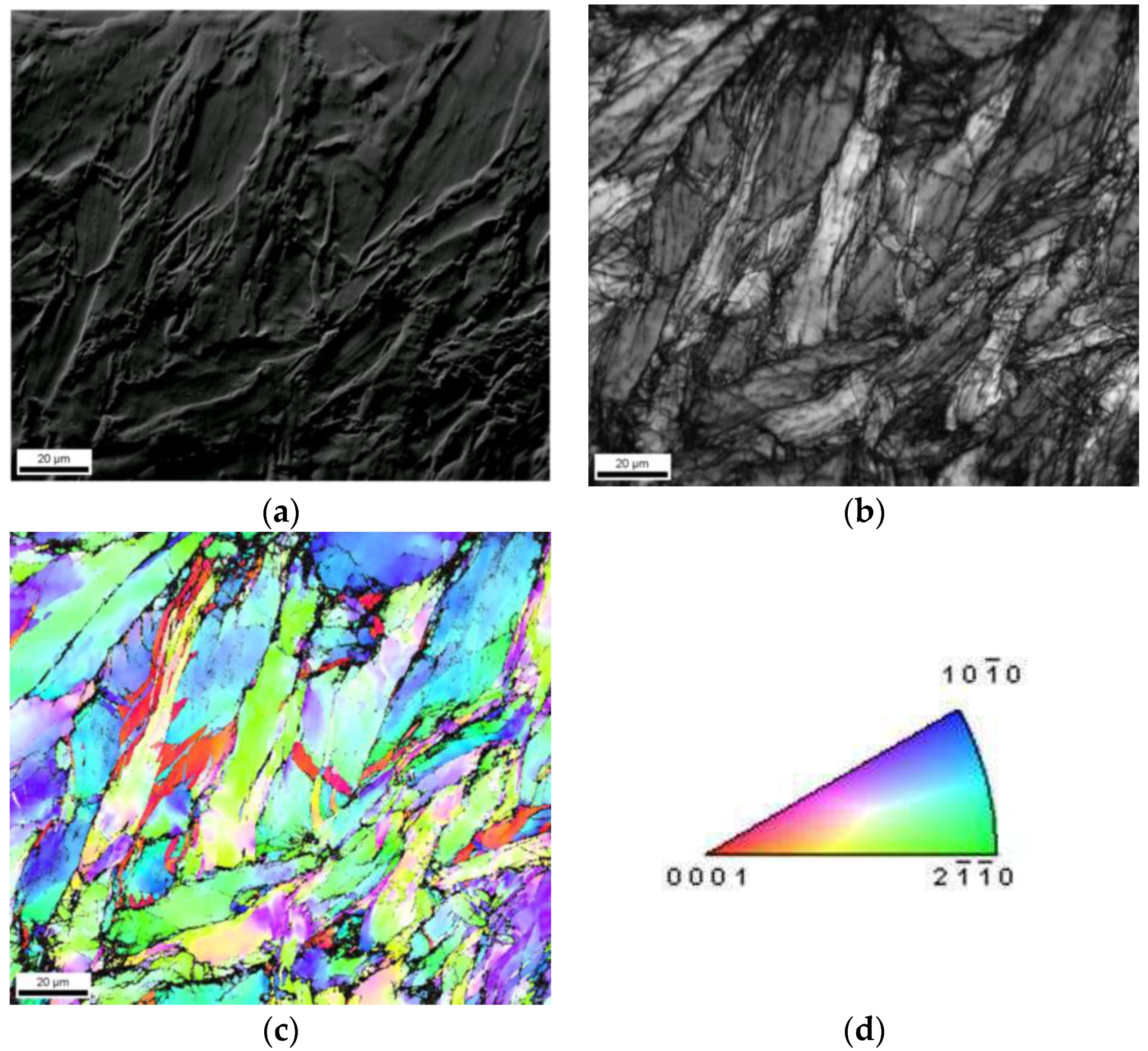
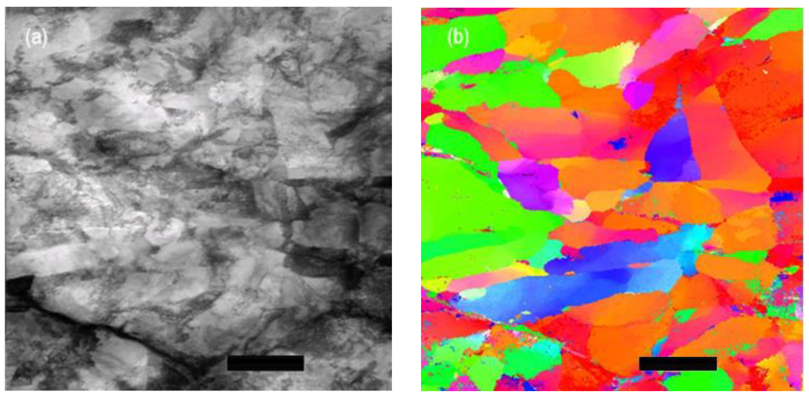
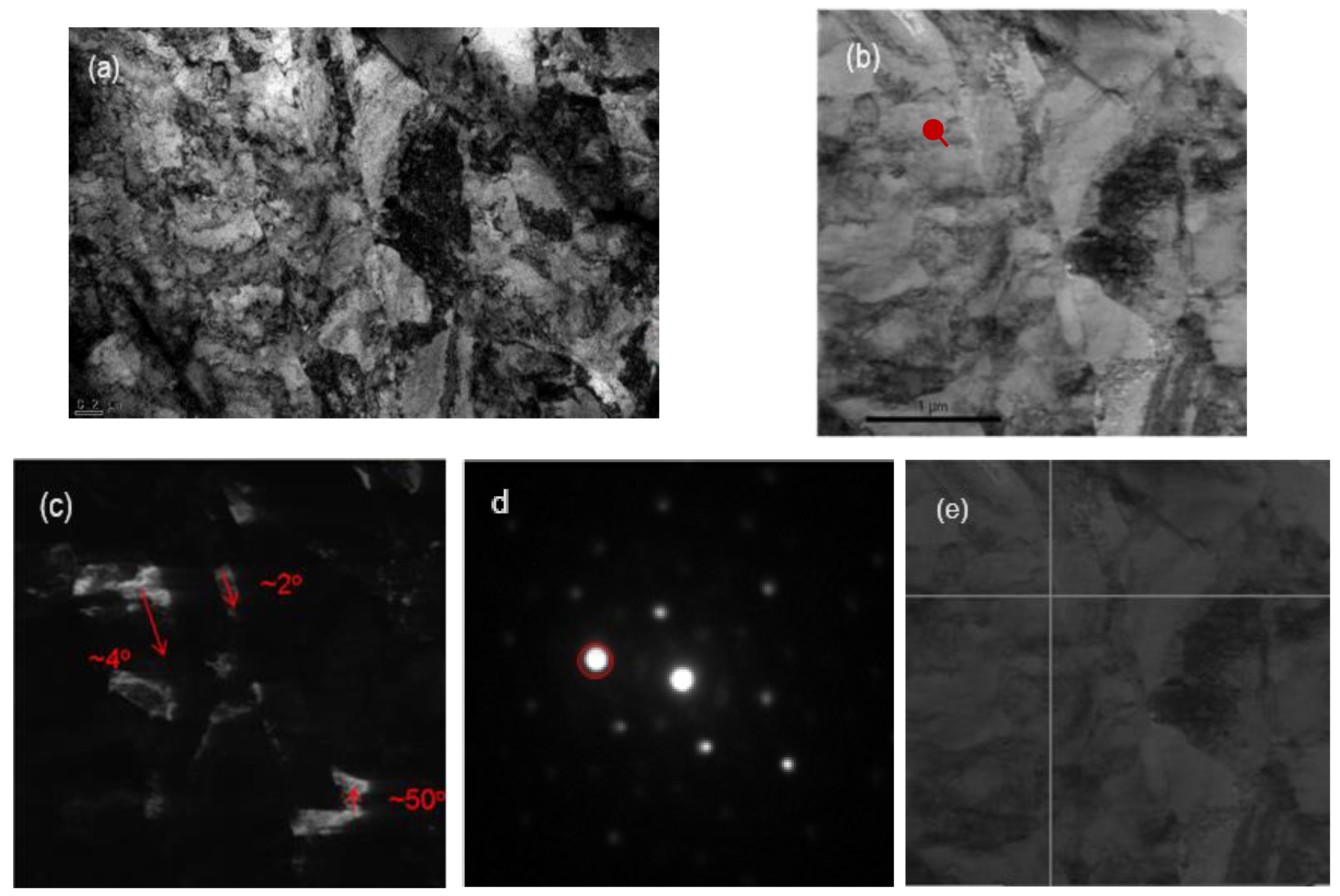
3. Results and Discussion
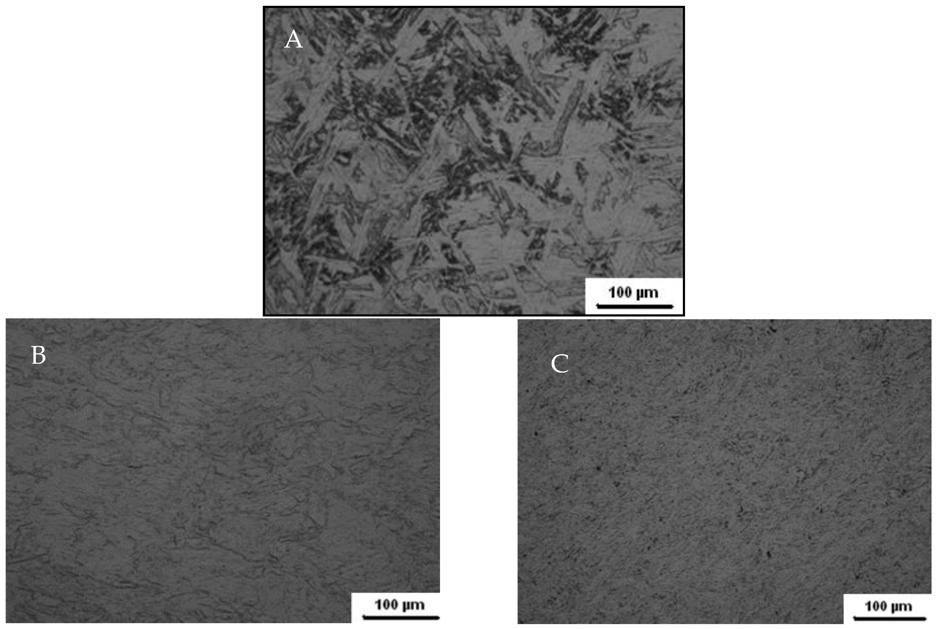
Light Microscopy

Light microscopy is shown in Figure 1 for annealed zirconium with a Widmanstätten structure (Figure 1A), and the images show the loss of this characteristic microstructure in the ECAE-processed samples deformed by one (Figure 1B) and four passes (Figure 1C).
The EBSD analysis of Zr deformed by 1 pass is shown in Figure 2. Plastic deformation occurred in a heterogeneous way. The microstructure was subdivided into shear bands, between which thinner division was only partially revealed through EBSD (Figure 2a,b). In these images, some twinning can also be observed. It is important to note that, compared with the level of detail given by the EBSD map (Figure 2c), the secondary electron image is poor in terms of the amount of information provided, as observed in the dark lines in Figure 2b. The quality map is a metric describing the quality of a diffraction pattern. It is constructed by mapping the value measured for each diffraction pattern obtained during an orientation imaging microscopy (OIM) scan to a gray or color scale.
The microstructure obtained after four ECAE passes is presented in Figure 3. The microstructure was still characterized by heterogeneity with micrometric and submicrometric grains that had the cross-shear characteristic of the Bc route, in which rotation occurs at 90° between passes in a counterclockwise direction. FEG-SEM/EBSD did not have the necessary resolution to define the microstructure in regions with a higher density of microstructure subdivision. Nevertheless, it seems clear that for Zr processed by ECAE, a greater number of passes is necessary to maybe achieve a homogeneous microstructure. This is in accordance with the study of [11], who still obtained a heterogeneous microstructure of titanium with 12 passes of high-temperature ECAE, as well as for magnesium in another work [12]. These authors attributed the heterogeneity to discontinuous recrystallization, and they also described that in titanium (and other hexagonal metals), the complex stress fields developed near the grain boundaries may activate additional slip/slip modes.
In order to better resolve the regions with a finer microstructure obtained with four passes, TEM samples were evaluated by TKD. The orientation maps obtained are shown in Figure 4. Although the resolution increased, parts of the microstructure remained unresolved. In both cases, EBSD and TKD, the level of unresolved points of the maps could be cleaned artificially, but it would decrease the confidence in any misorientation or grain boundary analysis.
The characterization by TEM of severely deformed microstructures is not easy to interpret, as discussed earlier. BF images, such as those presented in Figure 5A, reveal the expected signs of plastic deformation, including a high density of dislocations, poor definition of grain boundaries, and a gradual change in contrast resulting from the gradual change in orientation. In Figure 5B–F, DF images made with a 30 μm objective aperture are given. This type of image gives a better picture of the microstructure than the BF image and may be used to estimate the grain size obtained. Furthermore, when a nanodiffraction map is used to construct an orientation map and the common 15° misorientation for defining a grain boundary is used, a different picture appears as grain sizes become clear.
In Figure 6a, a reconstructed virtual BF image based on the map given in Figure 2d is presented. When this is performed, grains appear clearer than in DF images. The reason for this can be understood when different virtual DF images are reconstructed, such as in Figure 5, as due to the size of the spot, there is a difference in grain sizes.
Darkfield images were reconstructed from areas where TEM brightfield images were obtained (Figure 7c). The size of the virtual objective aperture used was equivalent to a 5 µm aperture, and the misorientation was evaluated in different lines, both inside and outside the highlighted grains. The DF image presented in Figure 7c was constructed using the marked spot, from a point at the dot. The orientations of the grains indicated with the arrows had 2°, 4° and 50° misorientation. Comparing these misorientation lines with the usual definition of a grain boundary, it is possible to see how a DF image has a lower correlation than the standard definition of a grain. The conclusion is that evaluating grain size from DF images requires many fields in order to statistically determine the true grain size.
The ACOM/TEM images in Figure 8 show reconstructed, virtual brightfield (BF) and darkfield images with nanodiffraction patterns that produced the results shown. The darkfield images can be plotted from a selection of spots and the size of the chosen virtual objective aperture.
Nanotexture seems to be crucial for accurate microstructure characterization. The results presented here show how the simple visualization of the microstructure cannot give a clear picture of its true properties. Furthermore, it is important to recall that the EBSD of bulk samples does not describe the microstructure of more refined regions, as reported by [13], who showed in their work that this technique does not possess the required spatial resolution to identify the ultrafine microstructure. Nanodiffraction mapping, on the other hand, does not suffer from this problem but needs a considerable number of fields due to the small field of view.
The microstructure of zirconium was deformed by ECAP after five passes [14], and the authors reported deformation heterogeneity of the grains and the banded structure within a single grain. In another study, a Zr-2.5Nb microstructure after four ECAP passes at 460 °C with an angle of 90° was carried out by [15]. The authors described an irregular grain–subgrain structure with submicron and nano sizes, a high density of dislocations, and large-angle boundaries by ring electron diffraction pattern. In another work, Zr-2.5Nb ECAPed samples with different temperatures and heating operations showed grain refinement to ultrafine grains [16]. The microstructure analysis was conducted with BF TEM image and SAD diffraction. Sklenicka (2012) [17] studied the microstructure of Zr-2.5Nb with EBSD, and they commented that the grain sizes were not fully investigated due to the limited resolution in the characterization of the very small grains by the EBSD method. An investigation of the formation of ZrO in the zirconium structure by TKD and TEM showed that they are complementary techniques [18].
These characterizations are very important nowadays since heterogeneous materials are a growing area in the metallurgy field. Wu and Zhu (2017) [19] defined heterogeneous materials as materials with strength heterogeneity, and they can be caused by microstructural heterogeneity, crystal structure heterogeneity, or compositional heterogeneity. The domain sizes can be in the range of micrometers to millimeters, and the domain geometry can vary to form very different material systems. So, different techniques can be used to correctly reveal the microstructure of these materials. The area of heterogeneous materials is an emerging field, and a combination of techniques can help the community to explain the mechanisms involved in the deformation of these materials.

4. Conclusions

EBSD revealed that the microstructure of ECAE-processed, fine-grain zirconium was heterogeneous, with a few large grains surrounded by a fine submicrometric structure that could only be partially resolved through this technique. This fine structure was described through nanodiffraction mapping on the TEM. Nevertheless, it lacks the field of view to properly characterize the microstructure. TKD is an intermediary technique due to its larger field of view, but it is still unable to completely describe the microstructure. Neither technique was fully adequate for the quantitative measurements of the samples. Another fundamental aspect revealed the shortcomings of the darkfield image in describing the grain structure of severely deformed samples. One way to overcome this problem is using a large number of fields of view, a procedure that is seldom mentioned in the literature as a standard practice.

Author Contributions

Conceptualization, M.V.P.C. and A.L.P.; methodology, M.V.P.C. and A.L.P.; software, M.F. and V.S., formal analysis, A.L.P.; investigation, M.V.P.C. and A.L.P.; resources, A.L.P., M.F. and V.S.; writing—original draft preparation, M.V.P.C.; writing—validation, review, and editing, A.-m.B.G.; supervision, A.L.P.; funding acquisition, A.L.P. All authors have read and agreed to the published version of the manuscript.

Funding

This research was funded by CNPq, grant number CNPq CNPQ 481096/2010-8.

Data Availability Statement

The raw data supporting the conclusions of this article will be made available by the authors on request.

Acknowledgments

The authors acknowledge CNPq and Finep (Brazil) for financial support and LABNANO/CBPF for the use of their TEM. The authors are grateful for the great contribution of Andre Luiz Pinto, who died in 2018, to develop this work and Cilene Labre for her support.

Conflicts of Interest

The authors declare no conflicts of interest.

References

  1. Pokropivny, V.V.; Skorokhod, V.V. New Dimensionality Classifications of Nanostructures. Phys. E Low-Dimens. Syst. Nanostruct. 2008, 40, 2521–2525. [Google Scholar] [CrossRef]
  2. Valiev, R.Z.; Langdon, T.G. Principles of Equal-Channel Angular Pressing as a Processing Tool for Grain Refinement. Prog. Mater. Sci. 2006, 51, 881–981. [Google Scholar] [CrossRef]
  3. Meyers, M.A.; Mishra, A.; Benson, D.J. The Deformation Physics of Nanocrystalline Metals: Experiments, Analysis, and Computations. JOM 2006, 58, 41–48. [Google Scholar] [CrossRef]
  4. Wu, G.; Zaefferer, S. Advances in TEM Orientation Microscopy by Combination of Dark-Field Conical Scanning and Improved Image Matching. Ultramicroscopy 2009, 109, 1317–1325. [Google Scholar] [CrossRef] [PubMed]
  5. Moeck, P.; Rouvimov, S.; Rauch, E.F.; Nicolopoulos, S.; Secula, E.M.; Seiler, D.G.; Khosla, R.P.; Herr, D.; Michael Garner, C.; McDonald, R.; et al. Automated Crystal Phase and Orientation Mapping of Nanocrystals in a Transmission Electron Microscope. In Proceedings of the Frontiers of Characterization and Metrology for Nanoelectronics: 2009, Albany, NY, USA, 11–15 May 2009; AIP: Melville, NY, USA, 2009; pp. 304–308. [Google Scholar]
  6. Segal, V.M. Materials Processing by Simple Shear. Mater. Sci. Eng. A 1995, 197, 157–164. [Google Scholar] [CrossRef]
  7. Valiev, R.Z. Structure and Mechanical Properties of Ultrafine-Grained Metals. Mater. Sci. Eng. A 1997, 234–236, 59–66. [Google Scholar] [CrossRef]
  8. Saldana, L.; Mendezvilas, A.; Jiang, L.; Multigner, M.; Gonzalezcarrasco, J.; Perezprado, M.; Gonzalezmartin, M.; Munuera, L.; Vilaboa, N. In Vitro Biocompatibility of an Ultrafine Grained Zirconium. Biomaterials 2007, 28, 4343–4354. [Google Scholar] [CrossRef] [PubMed]
  9. Nathaniel, J.E.; Lang, A.C.; El-Atwani, O.; Suri, P.K.; Baldwin, J.K.; Kirk, M.A.; Wang, Y.; Taheri, M.L. Toward High-Throughput Defect Density Quantification: A Comparison of Techniques for Irradiated Samples. Ultramicroscopy 2019, 206, 112820. [Google Scholar] [CrossRef] [PubMed]
  10. Mu, X.; Kobler, A.; Wang, D.; Chakravadhanula, V.S.K.; Schlabach, S.; Szabó, D.V.; Norby, P.; Kübel, C. Comprehensive analysis of TEM methods for LiFePO4/FePO4 phase mapping: Spectroscopic techniques (EFTEM, STEM-EELS) and STEM diffraction techniques (ACOM-TEM). Ultramicroscopy 2016, 170, 10–18. [Google Scholar] [CrossRef]
  11. Dyakonov, G.S.; Mironov, S.; Semenova, I.P.; Valiev, R.Z.; Semiatin, S.L. Microstructure Evolution and Strengthening Mechanisms in Commercial-Purity Titanium Subjected to Equal-Channel Angular Pressing. Mater. Sci. Eng. A 2017, 701, 289–301. [Google Scholar] [CrossRef]
  12. Krywopusk, N.M.; Kecskes, L.J.; Weihs, T.P. Microstructural Characterization of Pure Mg and AZ31B Processed by ECAE. Mater. Charact. 2019, 158, 109950. [Google Scholar] [CrossRef]
  13. Proust, G.; Trimby, P.; Piazolo, S.; Retraint, D. Characterization of Ultra-Fine Grained and Nanocrystalline Materials Using Transmission Kikuchi Diffraction. JoVE 2017, 122, e55506. [Google Scholar] [CrossRef] [PubMed]
  14. Lee, B.S.; Kim, M.H.; Hwang, S.K.; Kwun, S.I.; Chae, S.W. Grain Refinement of Commercially Pure Zirconium by ECAP and Subsequent Intermediate Heat Treatment. Mater. Sci. Eng. A 2007, 449–451, 1087–1089. [Google Scholar] [CrossRef]
  15. Nikulin, S.A.; Rogachev, S.O.; Rozhnov, A.B.; Gorshenkov, M.V.; Kopylov, V.I.; Dobatkin, S.V. Resistance of Alloy Zr-2.5% Nb with Ultrafine-Grain Structure to Stress Corrosion Cracking. Met. Sci. Heat Treat. 2012, 54, 407–413. [Google Scholar] [CrossRef]
  16. Nikulin, S.A.; Rozhnov, A.B.; Rogachev, S.O.; Khatkevich, V.M.; Turchenko, V.A.; Khotulev, E.S. Investigation of Structure, Phase Composition, and Mechanical Properties of Zr-2.5% Nb Alloy after ECAP. Mater. Lett. 2016, 169, 223–226. [Google Scholar] [CrossRef]
  17. Sklenicka, V.; Dvorak, J.; Kral, P.; Svoboda, M.; Kvapilova, M.; Kopylov, V.I.; Nikulin, S.A.; Dobatkin, S.V. Creep Behavior of a Zirconium Alloy Processed by Equal-Channel Angular Pressing. Acta Phys. Pol. A 2012, 122, 485–489. [Google Scholar] [CrossRef]
  18. Sneddon, G.C.; Trimby, P.W.; Cairney, J.M. Transmission Kikuchi Diffraction in a Scanning Electron Microscope: A Review. Mater. Sci. Eng. R Rep. 2016, 110, 1–12. [Google Scholar] [CrossRef]
  19. Wu, X.; Zhu, Y. Heterogeneous materials: A new class of materials with unprecedented mechanical properties. Mater. Res. Lett. 2017, 5, 527–532. [Google Scholar] [CrossRef]
Figure 1. Light micrographs of Zr (A) annealed and deformed by 1 (B) and (C) 4 ECAE passes, both in longitudinal section. Scale bar 100 µm.
Metals 14 00624 g001
Figure 2. FEG-SEM/EBSD micrographs of Zr deformed by 1 ECAE pass: (a) secondary electron image, (b) indexation quality map, (c) orientation map, (d) color reference for inverse pole figure. Scale bar 20 µm.
Metals 14 00624 g002
Figure 3. FEG-SEM/EBSD micrograph of Zr deformed by 4 ECAE passes: (a) indexation quality map and (b) orientation map. Scale Bar—10 µm.
Metals 14 00624 g003
Figure 4. TKD/FEG-SEM micrograph of Zr deformed by 4 ECAE passes: (a) band contrast map and (b) orientation map.
Metals 14 00624 g004
Figure 5. (A) TEM brightfield image of Zr deformed by 4 ECAE passes at 350 °C, (BF) TEM darkfield images of 4 ECAE passes at 350 °C reconstructed with different diffraction spots and virtual apertures. Scale bar—200 nm.
Metals 14 00624 g005
Figure 6. ACOM/TEM micrograph of Zr deformed by 4 ECAE passes: (a) virtual brightfield image and (b) orientation map. Scale bar—1 µm.
Metals 14 00624 g006
Figure 7. (a) Brightfield TEM image of Zr deformed by 4 ECAE passes, (b) virtual brightfield image from a nanodiffraction mapping of the same region. The red dot is the area where nanodiffraction was done. (c) Virtual darkfield showing with red arrow misorientations of the grains, (d) nanodiffraction with the aperture location marked with a red circle from the intersection of lines shown in the (e) virtual brightfield image. Scale bar 1 µm.
Metals 14 00624 g007
Figure 8. (a) Nanobeam diffraction and virtual selection of spots (red circle) of Zr processed by 4 passes at 350 °C and virtual brightfield image. (b) Nanobeam diffraction and virtual selection of spots (red circle) of Zr processed by 4 passes at 350 °C and virtual darkfield image. (c) Nanobeam diffraction and virtual selection of spots (red circle with area greater than (b)) of Zr processed by 4 passes at 350 °C and virtual darkfield image. Scale bar—1 µm.
Metals 14 00624 g008
Disclaimer/Publisher’s Note: The statements, opinions and data contained in all publications are solely those of the individual author(s) and contributor(s) and not of MDPI and/or the editor(s). MDPI and/or the editor(s) disclaim responsibility for any injury to people or property resulting from any ideas, methods, instructions or products referred to in the content.

