Article

Metallurgical Defects and Roughness Investigation in the Laser Powder Bed Fusion Multi-Scanning Strategy of AlSi10Mg Parts

1
Department of Mechanical and Aerospace Engineering DIMA, Sapienza University of Rome, Via Edossiana 18, 00184 Rome, Italy
2
Department of Chemical, Material and Environmental Engineering DICMA, Sapienza University of Rome, Via Eudossiana 18, 00184 Rome, Italy
*
Author to whom correspondence should be addressed.
Metals 2024, 14(6), 711; https://doi.org/10.3390/met14060711
Submission received: 8 May 2024 / Revised: 1 June 2024 / Accepted: 13 June 2024 / Published: 16 June 2024
(This article belongs to the Special Issue Progress in Laser Advanced Manufacturing)

Abstract

:
Laser Powder Bed Fusion is the most attractive additive manufacturing technology for its capability to produce metal components with complex geometry. One of the main drawbacks is the poor surface roughness. In this work, different scan strategies and process parameters were studied and their effect on surface roughness, alloy microstructure, and metallurgical defects were discussed. The results highlighted that only tailored process conditions could combine acceptable roughness and absence of metallurgical defects. For the upskin, it has been seen that, although by increasing the Volumetric Energy Density value the Ra decreases, Volumetric Energy Density values higher than 69 J/mm3 determine meltpool instability with consequent formation of gas defects in the subsurface area. Similarly, by increasing the Linear Energy Density value, the Ra of the lateral surfaces decreases, but above 0.37 J/mm, metallurgical defects form in the subsurface area. This study also highlighted that the proposed process involves only a contained increase of the production times. In fact, the evaluation of the increased production times, related to the adoption of this multi-scanning strategy, is of fundamental importance to consider if the proposed process can be advantageously applied on an industrial scale.

1. Introduction

Among the different additive manufacturing (AM) technologies, the Laser Powder Bed Fusion (LPBF) is the most valued by the industries for its capability to produce layer by layer functional metallic components. It offers many advantages, such as no geometrical complexity limitations, the possibility to realize lightweight engineered parts, the absence of tooling, the reduction or the complete elimination of the assembly operations, and the minimization of the material waste. Notwithstanding the numerous advantages provided by this technology, one of the major drawbacks remains the obtainable surface roughness, which is a critical aspect to consider.
Optimizing the scanning strategies and process parameters of the LPBF process can improve both the metallurgical quality and the roughness of the part. Several studies available in the literature investigated the effect of scanning parameters [1] that have a significant impact on the part roughness and the microstructure of the alloy. As far as the surface roughness is concerned, smaller hatch distance can result in reduced roughness due to higher overlap between adjacent laser tracks [2]. The scan speed also affects the surface quality. Higher scan speed can produce a lower surface roughness, but it increases the chance to break into several parts due to Rayleigh instability [3]. In addition to that, it is important to note that the scan strategy can affect the alloy microstructure, resulting from modifying the melt pool temperature, the cooling rates, and the thermal cycling during manufacturing [4]. All this in turn affects the grain growth mechanism, commonly resulting in a variety of cellular/dendritic microstructures, thereby altering the physical and mechanical properties of the alloy [5]. Improper scan strategies can introduce defects such as lack of fusion, porosity, or balling [6]. A significant impact on the surface part quality is given by the combined effect of the process parameters rather than the single factor. In [7], the effects on upskin surface roughness of contouring process parameters, such as the laser power, the scanning speed, and the contour offset, for various surface slopes were studied through a full factorial plan. The results demonstrated that all the parameters are significant, and the best combinations were obtained at high Linear Energy Density (LED), e.g., at high laser power and low scan speed values. In [8], it was found that the contour scans have a more relevant influence than the inskin scan strategy on the roughness of inclined surfaces. Also, in [9], the process parameters involved in the contour strategy (namely the laser power, the scan speed, and the contour offset) were studied, showing that they have a primary role for the roughness of inclined, upskin, and downskin surfaces. Ren et al. [10] highlighted that the process parameters application order plays a significant role in the inclined surface final roughness. The results showed that a pre-contour strategy provides a lower roughness than a standard contour scanning.
In [11], the effects of various processing parameters (laser power, scanning speed, hatch distance, and beam offset) on the upfacing skin surface roughness of AlSi10Mg alloy were investigated. The applied optimization method permitted to reach a surface roughness of 5.4 μm through the use of a very low laser power at low speed and eliminating the laser partition track. However, these conditions can lead to residual stresses, high production time, and undesired microstructure that must be investigated.
The specific effects of the scan strategies on the roughness and microstructure of the part can vary depending on the alloy composition, hence extensive optimization of the scan strategy is often required to achieve the desired part roughness and microstructural characteristics. For these reasons, other approaches are necessary.
A different approach to improve the part quality and microstructure suggests the use of post-processing techniques after the LPBF fabrication. Different methods have been tested with different effects on the surface integrity, porosity, and residual stresses of LPBF parts [12]. Hot isostatic pressing is considered as the most effective way to remove pores in LPBF components improving their fatigue performance [13], but the roughness remains relevant due to the formation of depressions on the surface after induced plastic deformation [14]. Shot peening can produce residual compressive stresses that improve fatigue resistance, but the surface quality remains poor [15]. Mass finishing techniques such as barrel finishing can be used to improve the surface quality of LPBF parts, but it is slow and typically limited to external surfaces [16]. Machining can be a useful method to improve surface quality without damaging the microstructure of the part, but limitations such as tool accessibility on complex geometries, vibration of thin walls during the machining operation, etc. limit its applicability on LPBF parts [17]. Chemical or electrochemical polishing can improve the surface quality also of internal channels and trabecular structures [18], but the use of aggressive electrolytes containing hydrofluoric and perchloric acid, which are strong, highly corrosive, and toxic acids, could damage the material [19]. Although some post-processing techniques are very promising, their application is generally expensive both in terms of time and costs and, in some cases, most of the AM benefits (such as no geometrical complexity limitation) are lost.
Another opportunity is the use of laser remelting inside the additive process that consists of applying multiple scanning on the fabricated layer in order to improve surface quality or to reduce defects [20]. However, it may alter the microstructure and mechanical properties of the material, and it may not be suitable for all materials. For this reason, it is essential to consider simultaneously the effect of laser remelting on both surface quality and metallurgical microstructure because the improvement of one of them is not always related to the improvement of the other. A recent review paper [21] summarized experiments on different metals and alloys to study the effects of laser remelting on mechanical and tribological properties. However, the main goal of this treatment is to reduce roughness and defects of the surface [20,22,23] that affect mainly the fatigue life of the component [24,25].
LPBF is widely used to produce AlSi10Mg components with a good strength-to-weight ratio. AlSi10Mg is a hypoeutectic alloy that can be additively manufactured due to its narrow solidification range, which makes the alloy less prone to hot cracking during cooling. The production of this alloy by means of additive manufacturing has been deeply investigated in literature because the refined grain structure, due to very high solidification rates, allows to obtain better mechanical properties in comparison with the same alloy produced by using traditional techniques. In fact, the extremely high cooling rates determine very fine microstructures that allow to obtain parts characterized by high strength, even in the as-built condition [26]. On the other hand, microstructural heterogeneities at the scale of the melt pool may have a detrimental effect on the alloy mechanical properties. For this reason, there are studies available in literature that investigate the influence of the local thermal cycle on the part mechanical properties [27,28,29]. Moreover, the effect of the Volumetric Energy Density (VED) on the keyhole formation, microstructural evolution, and associated mechanical properties of AlSi10Mg fabricated by SLM has been deeply investigated. This study highlighted that the strength of SLM specimens is more than 70% higher than those of as-cast specimens, with an acceptable decrease of ductility [30].
The aim of this work is to evaluate the effect of a remelting methodology, in which scan strategies and process parameters are varied, on the obtainable surface roughness. The superficial and subsuperficial microstructure and defects of LPBF parts are investigated and correlated with the suggested processing conditions. The scanning methodology consists in the modifications of standard scan strategies and process parameters to perform an in-process treatment of the fabricated surfaces by multiple laser scanning. The novelty of the work lies in the employment of an industrial processing parameters set, which is characterized by high laser power and high scanning speed. The work strives to understand how to balance the improvement in term of surface roughness quality with the obtainable microstructure modifications and defects by applying a method that marginally alters the desired high productivity.

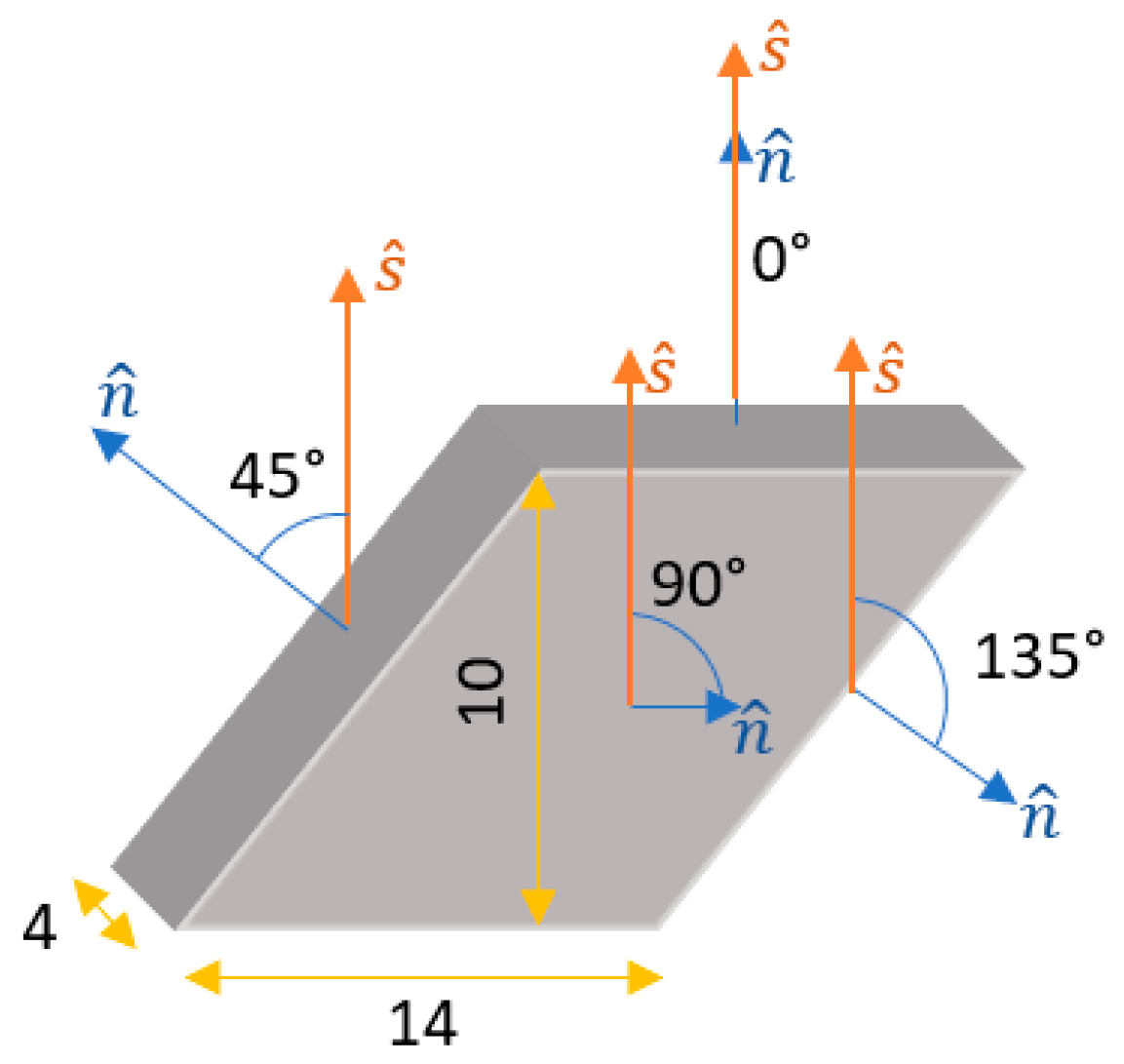
2. Materials and Methods

A specimen having the shape of an oblique rhombic prism was developed in Rhinoceros 7.0. This geometry was selected in order to have, on the same specimen, surfaces characterized by different slopes. The vector s ^ indicates the stratification direction and vector n ^ the normal to the surface, as shown in Figure 1. The local stratification angle is defined as the angle between s ^ and n ^ . The horizontal surfaces, namely the surfaces having a 0° local stratification angle, are the upskin surfaces. The other surfaces included in this geometry are 45°, 90°, and 135°.
The geometry was converted in standard triangulation language and pre-processed in Materialize Magics 23.01 (Materialise NV, Leuven, Belgium). The building preparation was provided in EOSPRINT 2.3. The specimens were oriented, in the x–y plane, by 5° to avoid problems with the recoater passage interaction and were placed in a fuzzy randomized position on the platform. The fabrication was realized by an EOSINT®M290 (EOS GmbH, Krailling, Germany) characterized by a building volume of 250 × 250 × 325 mm3 and a 400 W ytterbium fiber continuum laser, with a beam spot diameter of 100 µm. The process was carried out in an argon inert atmosphere with less than 0.1% oxygen. The building platform was preheated at 200 °C. The selected material is the AlSi10Mg provided by the machine manufacturer (EOS GmbH, Krailling, Germany) [31].
All the specimen surfaces were measured by means of a Mitutoyo SJ-412 profilometer (Kawasaki, Japan). It is equipped with a 180 mm length stylus with a 2.5 µm diamond tip allowing a vertical maximum height of 2400 µm necessary to detect the downskin surfaces. The measuring length was set to 10 mm. The acquired profiles were filtered by using a spline filter in accordance with ISO 16610-22 [32] and the average roughness was calculated in accordance with the ISO 4287 [33]. For this purpose, the cutoff and short wavelength cutoff were set to 2.5 µm and 8 µm, respectively. Moreover, the produced specimens were inspected using an optical microscope and a scanning electron microscope (SEM) (Hitachi High-Tech Corporation, Hitachinaka, Japan). The internal microstructure was analyzed so that the 0° and 90° sections could be studied. These two sections were grinded, polished with 0.5 µm alumina, and the surfaces were etched by using the Weck’s reagent to highlight the alloy microstructure.
The proposed methodology considers different scan strategies and involves the process parameters. The scanning consists of two main operations: the hatch, which is used to fabricate the inner volume of the layer, and the contour, employed to process the layer perimeter. The hatching strategy is referred to three different zones called infill or core, upskin, and downskin. Each strategy is characterized by different process parameters. In this experimentation the effects of the process parameters for contour and upskin strategies were investigated. In particular, the upskin one influences the surface quality of the horizontal surfaces characterized by a 0° local stratification angle. The contour strategy fabricates the perimeter of each layer: since the external skin of vertical and inclined surfaces is constituted only by perimeters, this strategy is used in the multi-scanning methodology to treat these surfaces. The hatching is not considered in the second scans of the methodology because the aim is to remelt only the external zones to maintain the unaltered part of the bulk material.
Each layer was processed in the following way:
  • The first scan (both for contour and hatching strategies) is used for the consolidation of the layer; it was performed using standard process parameters for the AlSi10Mg material suggested by EOS GmbH (machine and powders supplier, Krailling, Germany), i.e., 370 W laser power, 30 μm layer thickness, 1300 mm/s scan speed, 180 μm hatch distance, and 200 °C building platform temperature;
  • A second scan was applied for each layer modifying the process parameters for contour and upskin strategies in order to treat, directly inside the fabrication process, the surfaces obtained through the first scan. This way, the proposed method is applied only to the external skin of the components maintaining the standard conditions for the core part to avoid microstructural and metallurgical changes inside the part.
The experimented process parameters were the laser power, the scan speed, and the hatch distance. The laser power manages the quantity of energy supplied to the powder bed that is necessary to completely melt the material. The scan speed regulates the solidification and melting rates. The hatch distance determines the overlapping of adjacent tracks within the layer which allows them to bond together by metallurgical bonding [34]. These process parameters are all involved in the multiple scan surfaces, i.e., the upskin, and are markedly inter-affected. The controllability of their combined effect is typically provided by considering the integrated factor Volumetric Energy Density (VED) defined as follows:
V E D = P u L   V u H d
The employed laser power Pu and scan speed Vu values are reported in Table 1 for the upskin second pass processing; the VED is reported as well.
On the other hand, the lateral surfaces, i.e., the contours, are characterized by individual line strategies and only laser power and speed are involved. In order to assess the combined effect of these parameters the Linear Energy Density (LED) is calculated, which is defined as:
L E D = P c V c
The employed laser power Pc and scanning speed Vc are reported in Table 1 together with the corresponding LED.
The other processing parameters of this second scanning were fixed: the hatch distance Hd and the contour offset Co were fixed to 0.18 mm and 0.06 mm, respectively. The layer thickness L was 30 μm.
The densification of the manufactured specimens was measured by using the Archimedes method. The part mass in air and in distilled water allowed to obtain the part density and the porosity was calculated.

3. Results and Discussion

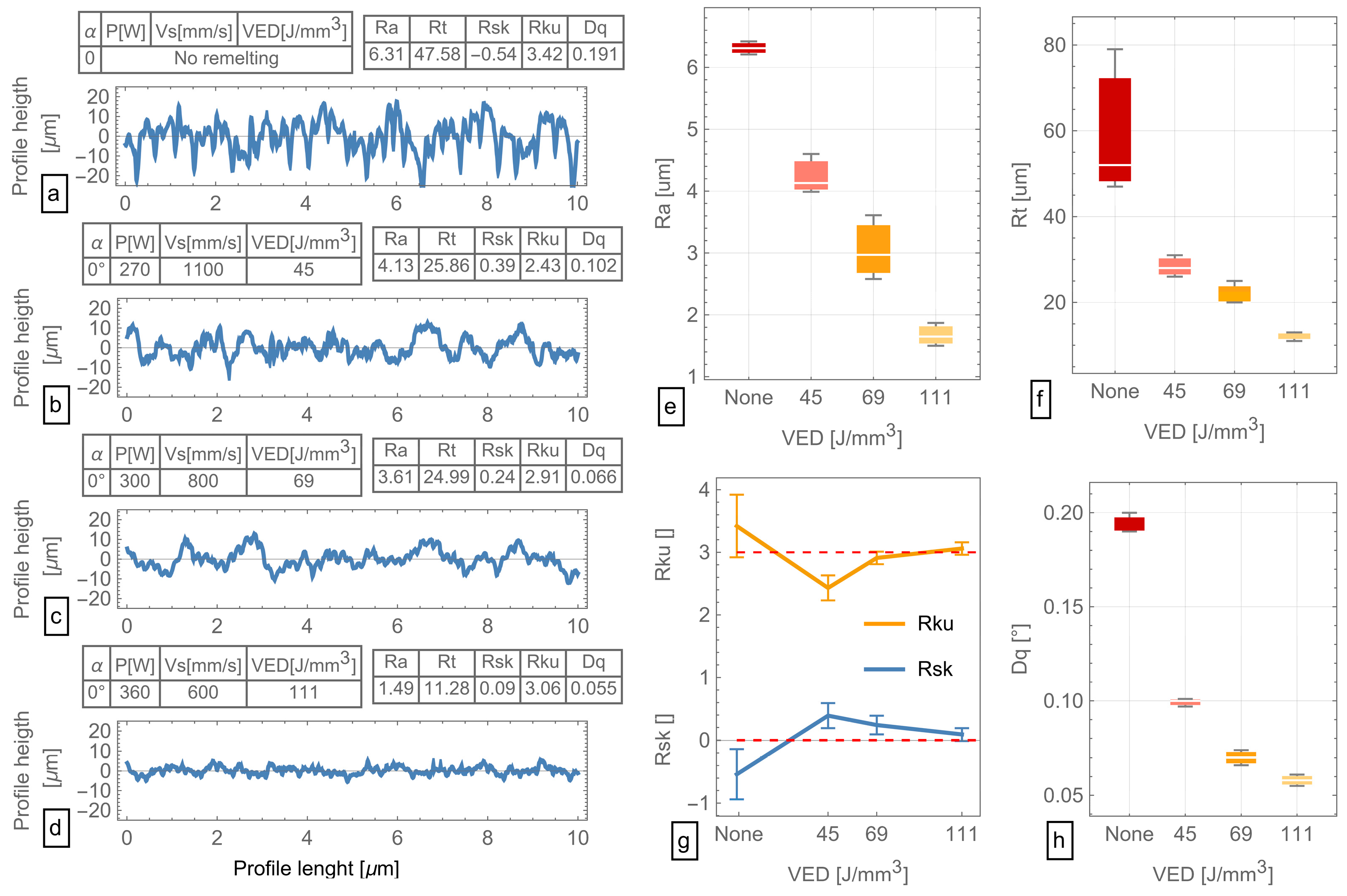
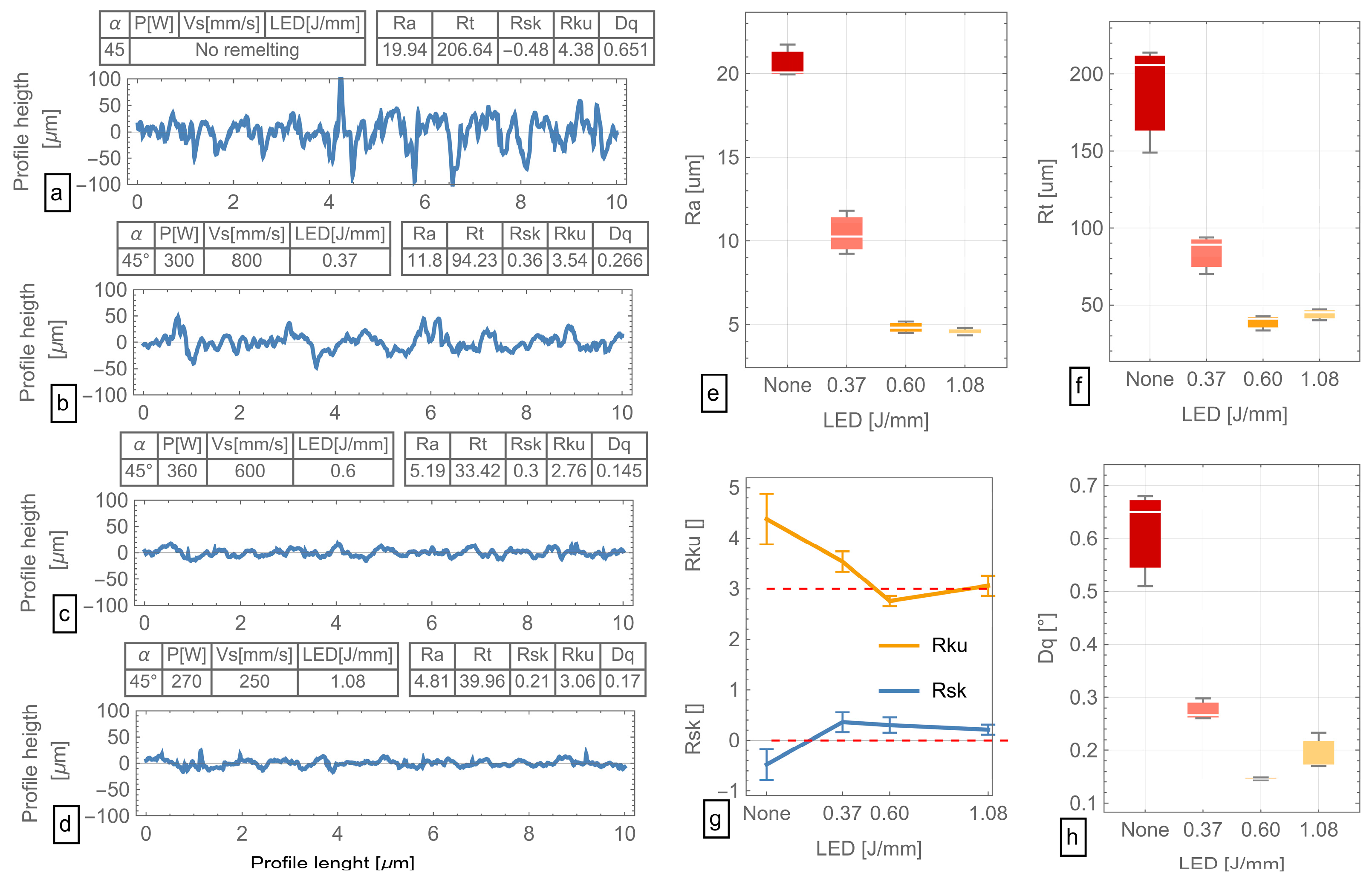
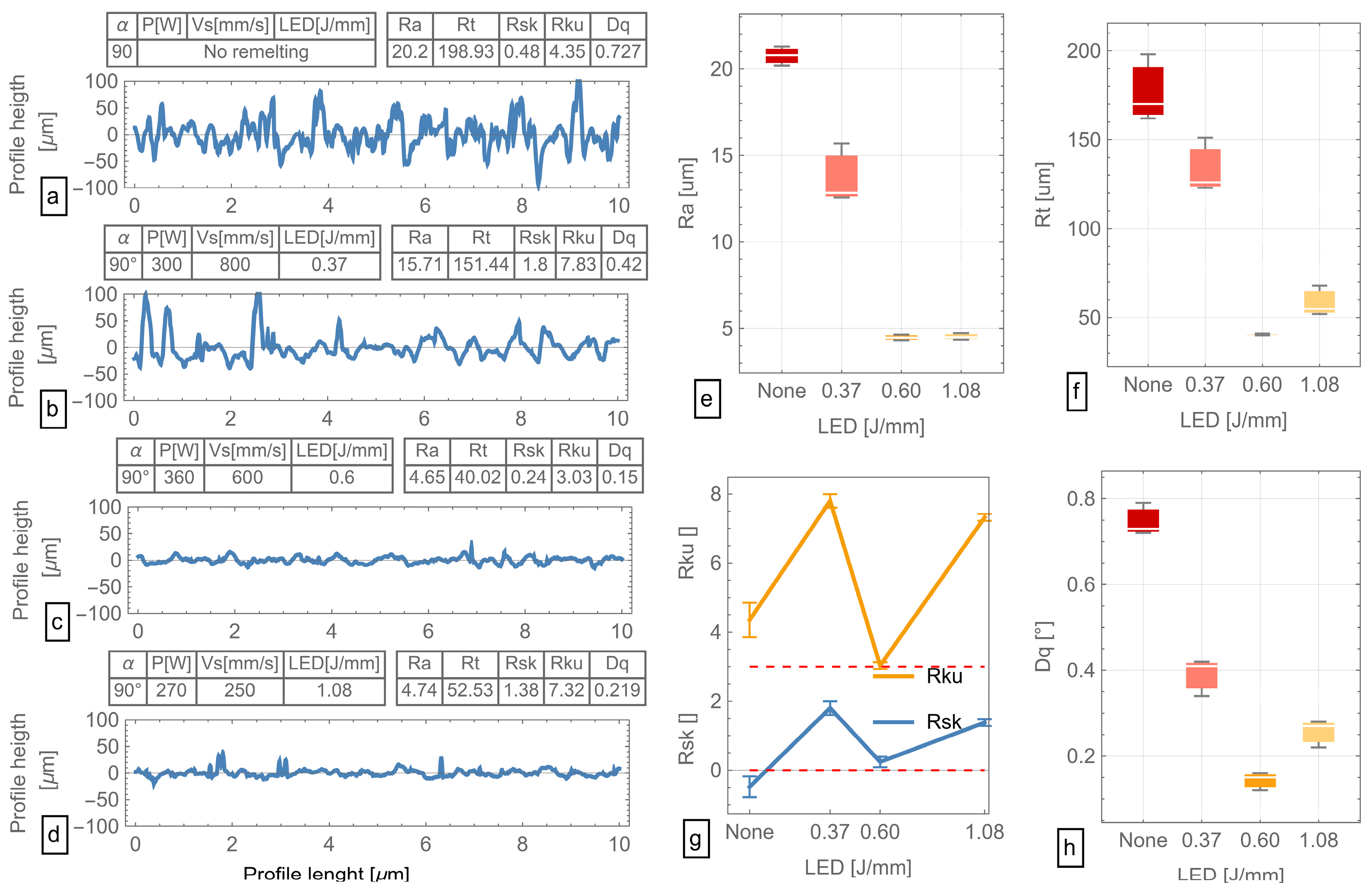
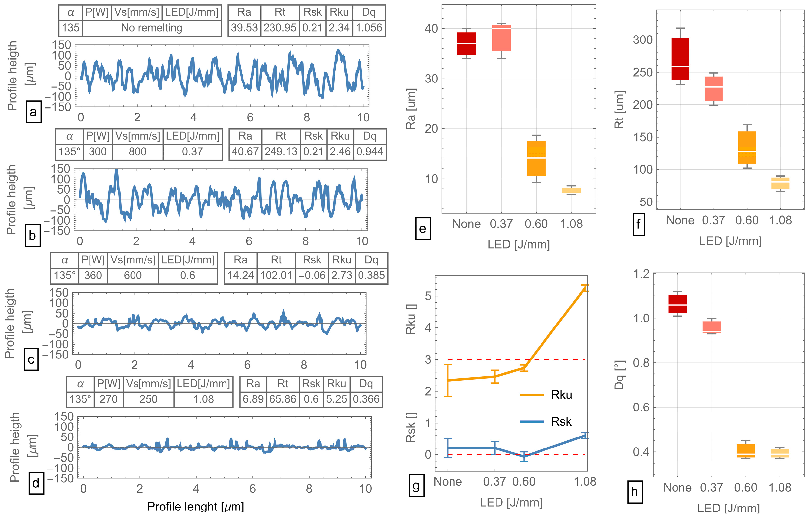
3.1. Roughness Evaluation

The first analysis investigated the micro-geometrical aspects of the fabricated specimens. The roughness profiles of 0° surfaces are shown in Figure 2a. The standard specimen exhibits a relatively low Ra and a peak to valley height is about 50 µm as expected for this slope and this alloy [35]. The shape of the height distribution can be described by the Rsk and Rku, which indicate the asymmetry and the sharpness of the roughness profile. The Rsk of −0.54 points out that the profile is made up by valleys with some peaks and the Rku, compared to the Gaussian distribution (Rku = 3), highlights a leptokurtic distribution, namely a profile with sharp peaks and valleys. This behavior well fits with the standard L-PBF morphology characterized by the slight presence of defects between tracks with sparse satellites and balling phenomena [36]. Finally, the Dq, namely the root mean square slope, indicates the root mean square of the local tilt along the sampling length. For the standard L-PBFed profile, it is 0.19°. The repetition of the measurements showed that the Ra and Dq have low scattering (first box plots in Figure 2e,h, respectively), while the Rt and shape parameters exhibit higher variability (first box plots in Figure 2f,g, respectively). This suggests that the valleys and peaks are not homogeneous on the surfaces processed by standard parameters set. As a remelting is applied the morphology of the roughness profile changes. In Figure 2b the specimen remelted by applying a VED of 45 J/mm3 is reported. The peaks are fused together and tend to fill the valleys rounding the shape in accordance with the observation of Yue et al. [37]. The Rsk is now positive and Rku tends to the kurtosis value of a circle arc which is approximatively 2.6. Nevertheless, the quality is partially improved as the Ra and Rt are 4.13 µm and 25.86 µm, respectively. The variability of these parameters is reduced. The material fusion provided a halving of the root mean square of the profile slope. A VED of 69 J/mm3 allowed to further decrease the Dq but the height roughness parameters slightly increased. Some peaks and valleys are still pronounced, and the shape of the profile now tends to the Gaussian shape with an Rku close to 3 and an Rsk of 0.24. At 111 J/mm3 VED the profile is now Gaussian and a marked reduction of all the roughness profile is obtained. Also, the scattering of the values is reduced. This is a satisfying result since it is probable that the morphology of the profile cannot be furtherly adjusted by the laser processing. In this case, the obtained final Ra is 76% less than the original surface processed via standard parameters.
The surface inclined by 45° shows a completely different trend. The original profile (see Figure 3a) exhibits a very high Rt with a variety of peaks and valleys. The Ra is about 20 µm generally affected by a marked balling phenomenon. In this case, the profile is mainly characterized by valleys and the height distribution is leptokurtic. By using remelting with an LED of 0.37 J/mm, the valleys depth is reduced as well as the peaks. Consequently, the Ra and Rt are halved, the Rsk is now positive and Rku is reduced (Figure 3b). At an increased LED of 0.60 J/mm, a further improvement is provided. The profile exhibits a quite flat trend with only 33.4 µm Rt and near Gaussian-shaped height distribution. As shown in Figure 3c the peaks are smooth and valleys almost disappeared. A similar result is obtained at 1.08 J/mm LED with a Gaussian distribution of the profile heights (Figure 3d). From the analysis of the Rsk trend, we can deduce that the symmetry of the height distribution is reached at high LED values (Figure 3g). The Ra graph confirms that the reduction of the Ra is greater than 75% at 0.60 or 1.08 J/mm LED (see Figure 3e). However, a little increase in the Rt is observed in Figure 3f at the highest LED level. Also, the presence of some local peaks affects the Dq which is 17% more than the previous LED level (Figure 3h). This suggests to not exceed 0.60 J/mm for the processing of a surface inclined by this angle.
The 90° surface slope is characterized by marked balling phenomena and not completely fused powder caused by the side effect of the laser consolidation process. The typical profile of such a surface is shown in Figure 4a: many marked peaks and some deep valleys can be observed. The average roughness and total roughness are about 20 µm and below 200 µm, respectively, in accordance with the results in [38]. The scattering of the provided measurements witnesses that the process is repeatable in terms of Ra (Figure 4e) while the defects are random causing a wide variation in the Rt (Figure 4f). Consequently, the shape of the profile is sharpened as evidenced by the Rku greater than 3 and the positive Rsk, which indicates that the profile is mainly composed by peaks. As remelting is applied at an LED value of 0.37 J/mm, the small to medium peaks are removed and the valleys are smoothened, as shown in Figure 4b. Conversely, bigger peaks are left unchanged: this behavior can be easily explained considering that they have bigger thermal modulus, and the given energy is not enough to provide the melting. The presence of some pronounced peaks determines an asymmetric (Rsk = 1.8) and a leptokurtic distribution with a very high Rku = 7.83. This soft processing provides a limited decreasing in terms of Ra and Rt as shown in Figure 4e,f, respectively. Moreover, an increased scattering is observed, thus suggesting the processing has low repeatability. The reduction of peaks and valleys makes the average slope of the profile decrease, as confirmed by the Dq, which is almost halved with respect to the original profile (Figure 4f). As an LED of 0.60 J/mm is employed, the obtained roughness profile shows a markedly improvement in terms of average and total roughness (Figure 4c). The energy provided to the surface is now enough to delete the most of the peaks and valleys and only few small asperities characterize the profile. The height distribution assumes a Gaussian shape as shown in Figure 4g, as the Rsk and Rku are about 0 and 3, respectively. This LED level allows reaching a 70% Ra reduction with a very small variability. A good result in terms of Ra is obtained also by applying 1.08 J/mm LED, but the Rt trend claims that some flaws affect now the profile (Figure 4f). As shown in Figure 4d, many narrow peaks are present leading to an increase of the Dq. This changing is measured by the Rsk, which is now positive, and Rku, which returned at a very high value (Figure 4g). These conditions suggest that 1.08 LED is too high for maintaining uniform surface quality in accordance with the trend found in [39].
The 135° slope surface is subjected to many undesired effects, since each layer is partially supported by the previous one. The dropping effect, i.e., the percolation of fused metal through the underlying powder, occurs and adds defects to the balling and satellite phenomena markedly present onto the inclined and vertical surfaces [40]. The manufacturer of the system typically tries to reduce these flaws by applying an increased LED to the main processing of the L-PBF process. By observing Figure 5a, big peaks and deep valleys are present and the positive Rsk and Rku of 2.34 suggest a shape close to a rounded profile, thus meaning that the increased energy amplifies the balling effect. The very high peak to valley height is reflected in the Dq which is higher than 1°. After a slight processing (i.e., 0.37 J/mm LED), the profile is not affected by noticeable modification (Figure 5b). The shape is almost the same as confirmed by the Rsk and Rku, the Ra is almost unchanged, and the Rt is marginally reduced, suggesting that some local peaks are still present. This LED level is not enough to change the 135° profile because of its coarse quality and rounded shape. In Figure 5c, the profile after applying 0.60 J/mm LED is shown. The behavior is completely changed in terms of profile peaks and valleys distribution: the heights are now symmetrical, and kurtosis indicates that they follow a Gaussian distribution. The Ra, which is markedly improved, exhibits a wider scattering over the measured specimens as compared to the previous cases (Figure 5e). The Dq is significantly reduced, as shown in Figure 5h. As a 1.08 J/mm LED is applied the profile is further improved (Figure 5d). The peaks are lowered and only few items are present: a reduction of more than 80% in Ra is provided with a very low scattering (Figure 5e). Analogously, the Rt has the same trend. As far as the shape parameters are concerned, the current energy is deeply modifying the profile: the Rsk is positive and a high Rku indicate that the profile is composed by few peaks over a relatively flat surface. Thus, the valleys appear to be reduced and, together with the few local peaks, provides a substantially unchanged Dq (Figure 5h). We can conclude that for 135° surfaces the highest LED level is advisable; however, an insight into the microstructure modification is necessary.

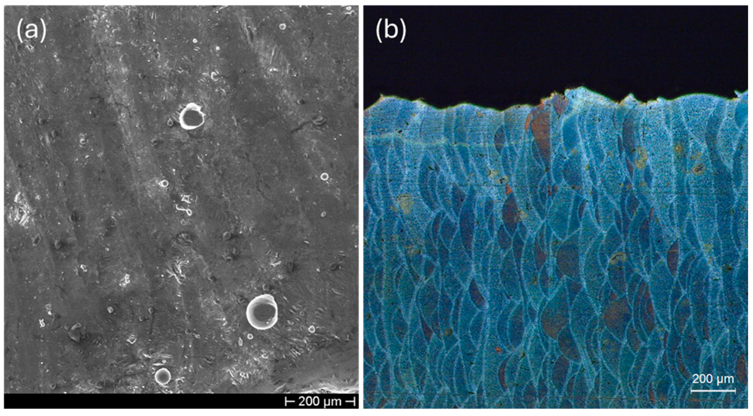
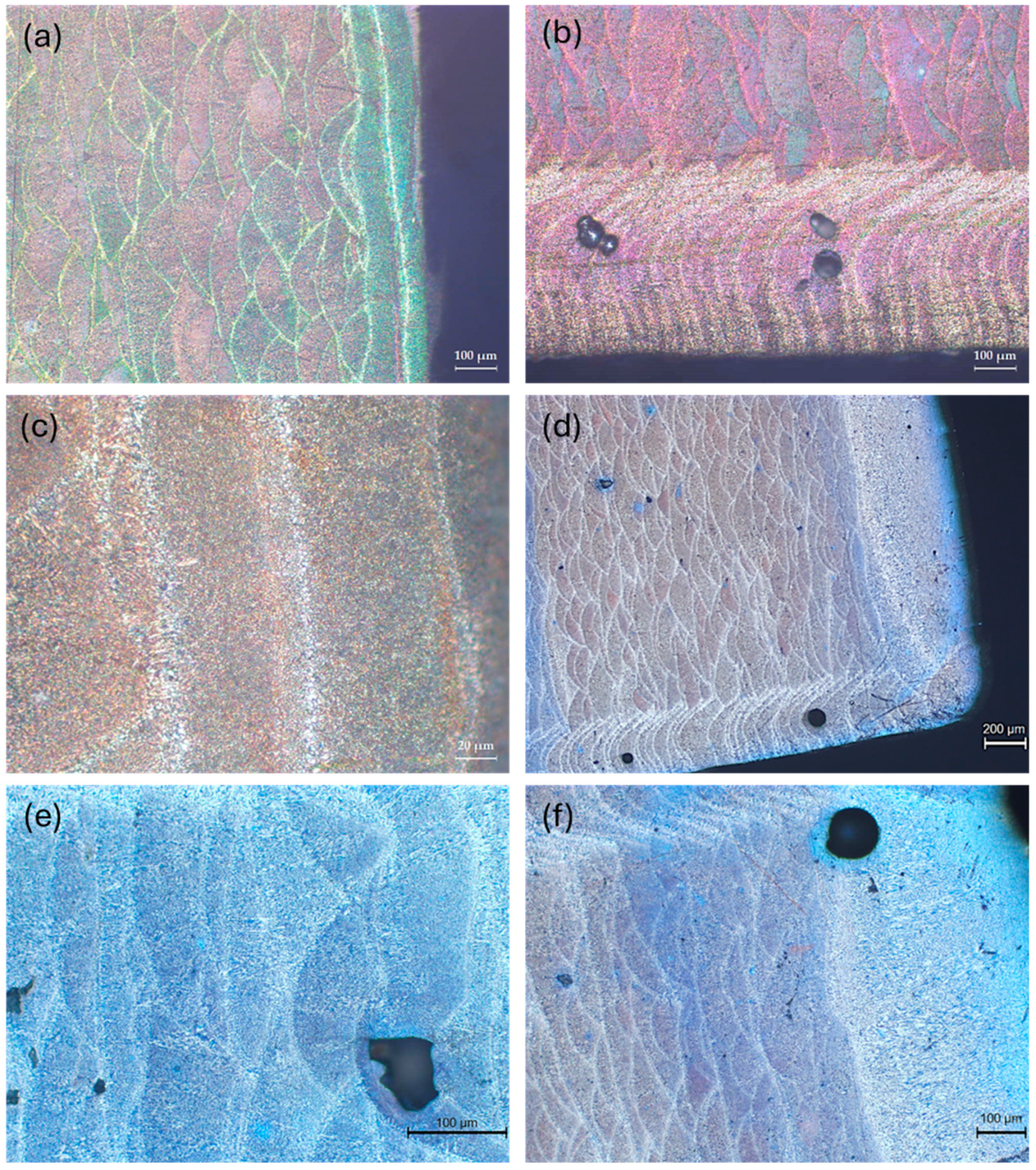
3.2. Microstructural and Defective Analyses

All the considerations about the surface roughness must be coupled with the study of the surface morphology and the microstructure of the samples. This is important in order to verify whether changing the scanning strategy results in a change in the microstructure or in the formation of metallurgical defects that could affect the mechanical properties of the alloy. Figure 6 shows the surface appearance of the specimen produced using the standard conditions (Figure 6a) and the texture of the standard specimen (Figure 6b) on the 90° section. It can be observed that while the bulk material, characterized by the typical fish-scale morphology, is compact, the surface shows the balling phenomenon that causes the measured roughness. It is well known from the literature [41] that the balling effect is induced by poor wettability of the molten alloy and by droplet splashing. During the production process, increasing the energy input can improve the wettability and avoid the balling effect. On the other hand, excessive energy input may determine balling effect due to droplet splashing. In this work, the remelting strategy has been applied to reduce the surfaces’ roughness.
Observing the specimen surfaces, it is possible to see that the presence of defects due to balling on the upskin decreases with increasing VED. This explains the previous findings. Figure 7 shows that the smoother surface is the one of specimen C, which appears almost defect free, as highlighted also by roughness measurements. On the other hand, process parameters affect cooling rates and then upskin microstructure: Figure 7c shows that the upskin of sample B is characterized by a dendritic microstructure.
In fact, by changing the VED used, not only there could be hydrodynamic instability inside the melting pool, but also different cooling rates that affect the alloy microstructure. This could be clarified by observing the microstructure of the specimen sections. Figure 8 shows optical micrographs taken on the 90° section of specimens A and C. The infill microstructure is characterized by the typical fish-scale morphology. Because of constitutional undercooling, the grains are columnar close to the boundaries, then, moving toward the center of the meltpool, they become dendritic and then equiaxed. Constitutional undercooling is related to a solute enriched layer at the interface between solid and liquid and the grain morphology depends on the G/R ratio, where G is the temperature gradient and R the solidification rate. During solidification thermal condition changes, in fact, initially the temperature gradient is very high and afterwards it decreases because thermal exchange becomes more difficult. This phenomenon affects the grain growth inside the meltpool. Moreover, the contour scan strategy influences its microstructure. Optical micrographs of the contour area show that LED values varying over the range 0.6–1.08 J/mm, which were able to smoothen the 90° external surface, produce the formation of gas defects (Figure 8b,d). As described by several authors [4,42], gas defects in LPBF can be determined by the Marangoni effect due to temperature gradient within the molten metal. In fact, the Marangoni effect is caused by mass shift due to the tension gradient that, within the melt pool, is due to the temperature gradient. The liquid metal flow, driven by the Marangoni effect, can trap gases within the molten pool, which cannot escape and remain in the solidified part.
The liquid flow can also affect the solidification process and determine the existence of points with locally delayed solidification, that produces microshrinkage defects evident in Figure 8e. A close observation of the upskin reveals that although high values of the VED (111 J/mm3) allow to have a smooth surface, it is characterized by the presence of gas defects mainly at the corners where there is a sudden change of the thermal module. Using a VED of 45.45 J/mm3, the thickness of the upskin is about 120 µm and it appears compact without gas defects (Figure 8a,c).
To mitigate gas defects in LPBF, process parameters can be optimized to minimize the occurrence of the Marangoni effect. Controlling the laser power and scan speed can help to improve the temperature distribution and surface tension gradients within the molten pool, reducing the likelihood of gas defects. By analyzing the optical micrographs of specimen B, it is possible to see that a decrease of the LED (0.37 J/mm) allowed to obtain a compact contour with only few microcavities (Figure 9). The upskin of specimen B has a thickness of about 200 µm: it has only few microcavities, while there are no gas defects because the low VED value mitigated the Marangoni effect. The micrograph in Figure 9c highlights that the thermal condition determined by the selected process parameters determined the formation of a prominent dendritic microstructure, which is also visible by performing a SEM observation of the upskin surface.
All these results show that in order to evaluate the effect of the scanning strategies on the produced component, it is important not only to evaluate the roughness but also to study the microstructure and the defective state of the parts. In particular, it is important to identify LED and VED values that allow to smoothen the surface without generating internal defects due to hydrodynamic instability.
The porosity measurements (Figure 10) confirmed the previous observations. The specimen manufactured by using the standard parameters exhibited a porosity ranging between 0.3% and 0.6% in accordance with the value of 0.4% claimed by the machine and material supplier [31]. The upskin surfaces, when treated by a slight VED, were characterized by an insignificant difference. As the VED increases, the mean porosity turns into 0.55% and 0.7% for 69 J/mm3 and 111 J/mm3, respectively. The contours processed by 0.37 J/mm and 0.6 J/mm LED showed minor increase of the porosity, while at 1.08 J/mm, some measurements reached 1%. These ascending trends are expected and in line with the previous considerations. Also, the overall porosity variability is generally limited since the remelting affects only a small volume just under the part skin.

3.3. Productivity Evaluation

The utilization of the standard processing parameters requires high laser power, high scanning speed, and high hatch distance, thus limiting the possibility to easily obtain a satisfying surface roughness without determining the formation of internal metallurgical defects. Although these conditions are hard to improve for this purpose, they result in a high productivity, which is an important aspect for the industrial utilization of this technology. For this reason, an additional processing should not significantly affect the total fabrication time.
For analyzing this aspect, some geometries were considered to evaluate the processing time for the different proposed combinations of the remelting parameters as compared to the standard industrial processing parameter set. The first geometry is the famous NIST test bench part [43] generally used to test AM technologies. In Figure 11, the used geometry is shown. The evaluation was accomplished by processing the STL file in the Materialise Magics 23.01 environment for the part orientation and support structure generation. These files were uploaded in EOSPRINT 2.3 platform. Here, the exposure parameters, namely the proposed strategies, were defined adding a contour and upskin/downskin hatch steps by selecting the laser power and speed values discussed in this paper, in accordance with Table 1. The simulation toolbox allowed to determine the total fabrication time for each combination. As shown in Figure 11 the setting of the standard parameter allowed to obtain the part in 526 min. For this geometry, the implementation of the presented strategy in the measure of a small LED and VED for the additional contour and upkin/downskin pass respectively required a total fabrication time of 540 min. In the graph, the normalized time as compared to the standard fabrication is reported. In this case, 3% additional time is needed. As the VED is increased, the additional time required is marginal. At 0.60 J/mm LED, the required time is almost the same at the investigated VED values. At the highest LED, the additional time ranges between 5% and 7%. This evaluation allows to have a quantitative output to decide the benefit of improving the outcoming surface directly during the fabrication process. Another interesting bench test geometry, typically employed for comparing the capability of AM technologies, is the reference part proposed by Minetola et al. [44]. This geometry is populated by many concave and convex shapes as well as holes and pins. Similarly to the previous case, by using the smallest LED and VED values for the additional contour and upkin/downskin passes respectively required, the total fabrication time increases only by 3%. At the highest LED and VED values, the fabrication time increases by about 9%. Fabrication times calculated for the aerospace jet engine bracket are very similar to the ones calculated for the NIST test bench. It is noteworthy that these increments are relatively small if compared with the utilization of a totally different technique to condition a not satisfying surface via a secondary operation (the part movement and fixturing, the setting of another process, and the operation time itself cannot be of the order of few minutes for a complicate geometry). This highlights that the choice of remelting parameters, usually based on the surface roughness obtainable on the component, cannot be completed regardless of production times and formation of metallurgical defects. For example, in this study, the best compromise between the surface roughness and the soundness of the component is obtained by using an LED of 0.37 J/mm and a VED of 69 J/mm3 in the remelting stage. These additional contour and downskin/upskin passes would require an additional production time ranging from 1 to 4%, which is very small in comparison with times required for performing additional different operations.

4. Conclusions

In this work, a multi-scanning strategy, applied by varying process parameters for contour and upskin strategies, was analyzed. The first scanning, used for the layer consolidation, was performed using standard process parameters, while a second one was applied for each layer, modifying the process parameters for contour and upskin strategies in order to treat only the external skin of the part. The investigation has been carried out with the aim of improving the surface roughness without altering the alloy integrity and microstructure.
The results highlighted that:
For the horizontal surfaces, the Ra was reduced by 76% with respect to the original surface, but VED values higher than 69 J/mm3 produce hydrodynamic instability with formation of gas defects in the subsurface area;
For surfaces characterized by a 45° local stratification angle, the proposed remelting strategy allowed to reduce the Ra from 20 µm to 5 µm; however, LED values greater than 0.60 J/mm cause a little increase of the Rt, which is a signal of excessive energy;
Similar outcomes are obtained on vertical surfaces, and the Ra starting at about 20 µm was modified down to 5 µm; also, in this case, it is advisable not to exceed 0.60 J/mm to avoid the generation of some superficial defects that determine an increase of the Rt as well as subsuperficial defects such as gas and microshrinkage pores produced by the Marangoni effect;
The downskin surfaces characterized by a slope of 135° present, in the standard condition, a very chaotic aspect due to the fact that each layer is only partially supported by the previous one.To reach a drastic reduction of the Ra, it is necessary to set a maximum LED value of 1.08 J/mm;
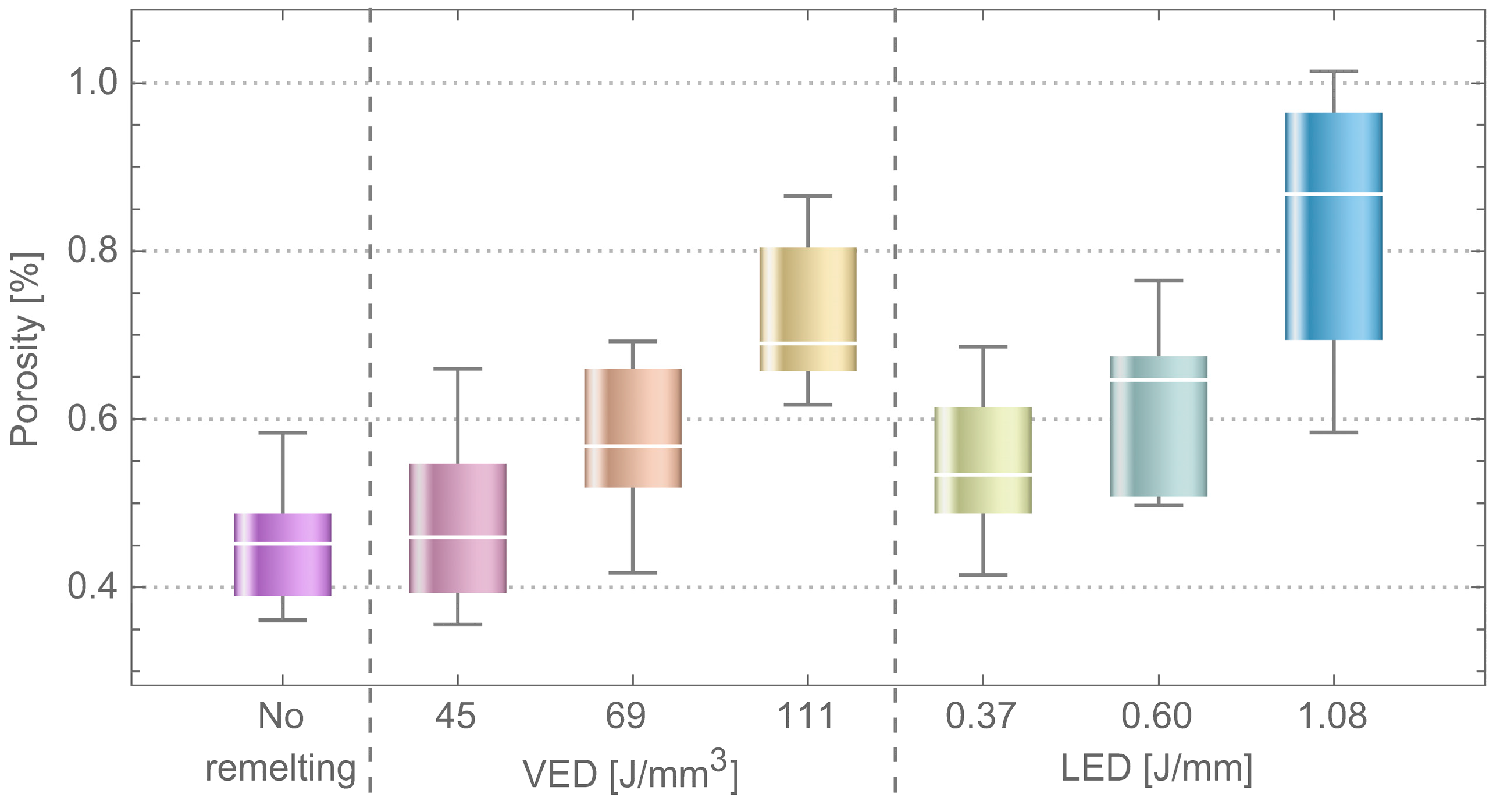
As expected, the additional scan causes the porosity to increase with the VED and LED values; however, the increase is within 1%, since the scan only processes the skin;
The production time to apply this multiscanning methodology calculated on some test bench geometries highlighted an increase of only some percentage points, confirming that the proposed methodology is affordable for industrial use.

Author Contributions

Conceptualization, A.B.; methodology, A.B. and L.B.; validation, D.P.; investigation, A.B. and D.P.; data curation, L.B.; writing—original draft preparation, L.B. and D.P.; funding acquisition, L.B. All authors have read and agreed to the published version of the manuscript.

Funding

Financed by the European Union—NextGenerationEU (National Sustainable Mobility Center CN00000023, Italian Ministry of University and Research Decree n. 1033-17/06/2022, Spoke 11-Innovative Materials & Lightweighting). The opinions expressed are those of the authors only and should not be considered as representative of the European Union or the European Commission’s official position. Neither the European Union nor the European Commission can be held responsible for them.

Data Availability Statement

The original contributions presented in the study are included in the article, further inquiries can be directed to the corresponding author. The data are not publicly available due to the ongoing nature of the study.

Conflicts of Interest

The authors declare no conflicts of interest.

References

  1. Kladovasilakis, N.; Charalampous, P.; Kostavelis, I.; Tzetzis, D.; Tzovaras, D. Impact of metal additive manufacturing parameters on the powder bed fusion and direct energy deposition processes: A comprehensive review. Prog. Addit. Manuf. 2021, 6, 349–365. [Google Scholar] [CrossRef]
  2. Islam, S.A.; Hao, L.; Javaid, Z.; Xiong, W.; Li, Y.; Jamil, Y.; Chen, Q.; Han, G. Surface Roughness of Interior Fine Flow Channels in Selective Laser Melted Ti-6Al-4V Alloy Components. Micromachines 2024, 15, 348. [Google Scholar] [CrossRef] [PubMed]
  3. Kumar, S. Additive Manufacturing Processes; Springer: Cham, Switzerland, 2020. [Google Scholar] [CrossRef]
  4. Krakhmalev, P.; Kazantseva, N. Microstructure of L-PBF alloys. In Additive Manufacturing Materials and Technologies, Fundamentals of Laser Powder Bed Fusion of Metals; Yadroitsev, I., Yadroitsava, I., Plessis, A.D., MacDonald, E., Eds.; Elsevier: Amsterdam, The Netherlands, 2021; pp. 215–243. [Google Scholar] [CrossRef]
  5. Biffi, C.A.; Fiocchi, J.; Bassani, P.; Tuissi, A. Continuous wave vs pulsed wave laser emission in selective laser melting of AlSi10Mg parts with industrial optimized process parameters: Microstructure and mechanical behaviour. Addit. Manuf. 2018, 24, 639. [Google Scholar] [CrossRef]
  6. Chowdhury, S.; Yadaiah, N.; Prakash, C.; Ramakrishna, S.; Dixit, S.; Gupta, L.R.; Buddhi, D. Laser powder bed fusion: A state-of-the-art review of the technology, materials, properties & defects, and numerical modelling. J. Mater. Res. Technol. 2022, 20, 2109. [Google Scholar] [CrossRef]
  7. Lea, T.N.; Rauniyara, S.; Ha, N.V.; Choua, K. An Investigation into the Effects of Contouring Process Parameters on the Up-skin Surface Characteristics in Laser Powder-Bed Fusion Process. Manuf. Lett. 2023, 35, 707. [Google Scholar] [CrossRef]
  8. Yang, T.; Liu, T.; Liao, W.; Wei, H.; Zhang, C.; Chen, X.; Zhang, K. Effect of processing parameters on overhanging surface roughness during laser powder bed fusion of AlSi10Mg. J. Manuf. Process. 2021, 61, 440. [Google Scholar] [CrossRef]
  9. Chen, Z.; Wu, X.; Tomus, D.; Davies, C.H.J. Surface roughness of Selective Laser Melted Ti-6Al-4V alloy components. Addit. Manuf. 2018, 21, 91. [Google Scholar] [CrossRef]
  10. Ren, Z.; Wei, D.; Wang, S.; Zhang, D.Z.; Mao, S. On the role of pre- and post-contour scanning in laser powder bed fusion: Thermal-fluid dynamics and laser reflections. Int. J. Mech. Sci. 2022, 226, 107389. [Google Scholar] [CrossRef]
  11. Gao, C.; Tang, H.; Zhang, S.; Ma, Z.; Bi, Y.; Rao, J.-H. Process Optimization for Up-Facing Surface Finish of AlSi10Mg Alloy Produced by Laser Powder Bed Fusion. Metals 2022, 12, 2053. [Google Scholar] [CrossRef]
  12. Ye, C.; Zhang, C.; Zhao, J.; Dong, Y. Effects of Post-processing on the Surface Finish, Porosity, Residual Stresses, and Fatigue Performance of Additive Manufactured Metals: A Review. J. Mater. Eng. Perform. 2021, 30, 6407–6425. [Google Scholar] [CrossRef]
  13. Günther, J.; Krewerth, D.; Lippmann, T.; Leuders, S.; Tröster, T.; Weidner, A.; Biermann, H.; Niendorf, T. Fatigue Life of Additively Manufactured Ti–6Al–4V in the Very High Cycle Fatigue Regime. Int. J. Fatigue 2017, 94, 236–245. [Google Scholar] [CrossRef]
  14. Molaei, R.; Fatemi, A.; Phan, N. Significance of Hot Isostatic Pressing (HIP) on Multiaxial Deformation and Fatigue Behaviors Additive Manufactured Ti-6Al-4V Including Build Orientation and Surface Roughness Effects. Int. J. Fatigue 2018, 117, 352–370. [Google Scholar] [CrossRef]
  15. Wycisk, E.; Emmelmann, C.; Siddique, S.; Walther, F. High Cycle Fatigue (HCF) Performance of Ti-6Al-4V Alloy Processed by Selective Laser Melting. Adv. Mater. Res. 2013, 816–817, 134–139. [Google Scholar] [CrossRef]
  16. Nalli, F.; Bottini, L.; Boschetto, A.; Cortese, L.; Veniali, F. Effect of industrial heat treatment and barrel finishing on the mechanical performance of Ti6AL4V processed by selective laser melting. Appl. Sci. 2020, 10, 2280. [Google Scholar] [CrossRef]
  17. Didier, P.; Le Coz, G.; Robin, G.; Lohmuller, P.; Piotrowski, B.; Moufki, A.; Laheurte, P. Consideration of SLM additive manufacturing supports on the stability of flexible structures in finish milling. J. Manuf. Process. 2021, 62, 213. [Google Scholar] [CrossRef]
  18. Ali, U.; Fayazfar, H.; Ahmed, F.; Toyserkani, E. Internal Surface Roughness Enhancement of Parts Made by Laser Powder-Bed Fusion Additive Manufacturing. Vacuum 2020, 177, 109314. [Google Scholar] [CrossRef]
  19. An, L.; Wang, D.; Zhu, D. Electrochemical polishing with glycol-based electrolyte of the curved internal channels fabricated via laser powder bed fusion. J. Manuf. Process. 2024, 117, 375. [Google Scholar] [CrossRef]
  20. Guan, J.; Wang, Q. The effect of a remelting treatment scanning strategy on the surface morphology, defect reduction mechanism, and mechanical properties of a selective laser-melted Al-based alloy. J. Mater. Sci. 2022, 57, 9807–9817. [Google Scholar] [CrossRef]
  21. Bukhari, S.M.A.; Husnain, N.; Siddiqui, F.A.; Anwar, M.T.; Khosa, A.A.; Imran, M.; Qureshi, T.H.; Ahmad, R. Effect of laser surface remelting on Microstructure, mechanical properties and tribological properties of metals and alloys: A review. Opt. Laser Technol. 2023, 165, 109588. [Google Scholar] [CrossRef]
  22. Boschetto, A.; Bottini, L.; Pilone, D. Effect of laser remelting on surface roughness and microstructure of AlSi10Mg selective laser melting manufactured parts. Int. J. Adv. Manuf. Technol. 2021, 113, 2739–2759. [Google Scholar] [CrossRef]
  23. Kang, N.; Verdy, C.; Coddet, P.; Xie, Y.; Fu, Y.; Liao, H.; Coddet, C. Effects of laser remelting process on the microstructure, roughness and microhardness of in-situ cold sprayed hypoeutectic Al-Si coating. Surf. Coat. Technol. 2017, 318, 355–359. [Google Scholar] [CrossRef]
  24. Chen, H.; Wang, X.; Ren, X. Size effect on fatigue performance of SLM-ed AlSi10Mg alloy: Role of defect size distribution. Int. J. Fatigue 2024, 182, 108163. [Google Scholar] [CrossRef]
  25. Qian, G.; Jian, Z.; Qian, Y.; Pan, X.; Ma, X.; Hong, Y. Very-high-cycle fatigue behavior of AlSi10Mg manufactured by selective laser melting: Effect of build orientation and mean stress. Int. J. Fatigue 2020, 138, 105696. [Google Scholar] [CrossRef]
  26. Shakil, S.I.; Hadadzadeh, A.; Amirkhiz, B.S.; Pirgazi, H.; Mohammadi, M.; Haghshenas, M. Additive manufactured versus cast AlSi10Mg alloy: Microstructure and micromechanics. Results Mater. 2021, 10, 100178. [Google Scholar] [CrossRef]
  27. Mertens, A.; Delahaye, J.; Dedry, O.; Vertruyen, B.; Tchuindjang, J.T.; Habraken, A.M. Microstructure and Properties of SLM AlSi10Mg: Understanding the Influence of the Local Thermal History. Procedia Manuf. 2020, 47, 1089–1095. [Google Scholar] [CrossRef]
  28. Yan, Q.; Song, B.; Shi, Y. Comparative study of performance comparison of AlSi10Mg alloy prepared by selective laser melting and casting. J. Mater. Sci. Technol. 2020, 41, 199–208. [Google Scholar] [CrossRef]
  29. Praneeth, J.; Venkatesh, S.; Krishna, L.S. Process parameters influence on mechanical properties of AlSi10Mg by SLM. Mater. Today Proc. 2023, in press. [Google Scholar] [CrossRef]
  30. Wu, H.; Ren, Y.; Ren, J.; Liang, L.; Li, R.; Fang, Q.; Cai, A.; Shan, Q.; Tian, Y.; Baker, I. Selective laser melted AlSi10Mg alloy under melting mode transition: Microstructure evolution, nanomechanical behaviors and tensile properties. J. Alloys Compd. 2021, 873, 159823. [Google Scholar] [CrossRef]
  31. EOS GmbH—Electro Optical Systems. Material Data Sheet EOS AluminiumAlSi10Mg; EOS GmbH—Electro Optical Systems: Krailling/Munich, Germany, 2014. [Google Scholar]
  32. ISO 16610-22; Geometrical Product Specifications (GPS)—Filtration—Part 22: Linear Profile Filters: Spline Filters. Available online: https://www.iso.org/obp/ui/#iso:std:iso:16610:-22:ed-1:v1:en (accessed on 7 May 2024).
  33. ISO 4287:1997/Amd.1:2009; Geometrical Product Specifications (GPS)—Surface Texture: Profile Method—Terms, Definitions and Surface Texture Parameters AMENDMENT 1: Peak Count Number. International Organization for Standardization. Available online: https://www.iso.org/obp/ui/#iso:std:iso:4287:ed-1:v1:amd:1:v1:en (accessed on 7 May 2024).
  34. Wang, D.; Yang, Y.; Liu, Y.; Bai, Y.; Tan, C. Study on Single-Track, Multi-track and Multi-layer Manufacturing. In Laser Powder Bed Fusion of Additive Manufacturing Technology, 1st ed.; Wang, D., Yang, Y., Liu, Y., Bai, Y., Tan, C., Eds.; Springer: Singapore, 2024; pp. 59–80. [Google Scholar]
  35. Limbasiya, N.; Jain, A.; Soni, H.; Wankhede, V.; Krolczyk, G.; Sahlot, P. A comprehensive review on the effect of process parameters and post-process treatments on microstructure and mechanical properties of selective laser melting of AlSi10Mg. J. Mater. Res. Technol. 2022, 21, 1141–1176. [Google Scholar] [CrossRef]
  36. Wang, L.; Wang, S.; Wu, J. Experimental investigation on densification behavior and surface roughness of AlSi10Mg powders produced by selective laser melting. Opt. Laser Technol. 2017, 96, 88–96. [Google Scholar] [CrossRef]
  37. Yue, D.; Zhang, X.; Li, D.; Li, Z.; Wang, Z.; Chen, B. Effect of remelting strategy on forming mechanism of selective laser melted AlSi10Mg. J. Mater. Res. Technol. 2024, 30, 4283–4293. [Google Scholar] [CrossRef]
  38. Pakkanen, J.; Calignano, F.; Trevisan, F.; Lorusso, M.; Ambrosio, E.P.; Manfredi, D.; Fino, P. Study of Internal Channel Surface Roughnesses Manufactured by Selective Laser Melting in Aluminum and Titanium Alloys. Metall. Mater. Trans. A 2016, 47, 3837–3844. [Google Scholar] [CrossRef]
  39. Poncelet, O.; Marteleur, M.; van der Rest, C.; Rigo, O.; Adrien, J.; Dancette, S.; Jacques, P.J.; Simar, A. Critical assessment of the impact of process parameters on vertical roughness and hardness of thin walls of AlSi10Mg processed by laser powder bed fusion. Addit. Manuf. 2021, 38, 101801. [Google Scholar] [CrossRef]
  40. Calignano, F. Design optimization of supports for overhanging structures in aluminum and titanium alloys by selective laser melting. Mater. Des. 2014, 64, 203–213. [Google Scholar] [CrossRef]
  41. Fu, J.; Li, H.; Song, X.; Fu, M.W. Multi-scale defects in powder-based additively manufactured metals and alloys. J. Mater. Sci. Technol. 2022, 122, 165–199. [Google Scholar] [CrossRef]
  42. Yang, G.; Xie, Y.; Zhao, S.; Qin, L.; Wang, X.; Wu, B. Quality Control: Internal Defects Formation Mechanism of Selective Laser Melting Based on Laser-powder-melt Pool Interaction: A Review. Chin. J. Mech. Eng. Addit. Manuf. Front. 2022, 1, 100037. [Google Scholar] [CrossRef]
  43. Moylan, S.; Slotwinski, J.; Cooke, A.; Jurrens, K.; Donmez, M. An Additive Manufacturing Test Artifact. J. Res. Natl. Inst. Stand. Technol. 2014, 119, 429–459. [Google Scholar] [CrossRef]
  44. Minetola, P.; Galati, M.; Calignano, F.; Iuliano, L.; Rizza, G.; Fontana, L. Comparison of dimensional tolerance grades for metal AM processes. Proc. CIRP 2020, 88, 399–404. [Google Scholar] [CrossRef]
Figure 1. Specimen geometry.
Metals 14 00711 g001
Figure 2. Roughness profile for 0° without remelting (a), where a VED of 45 J/mm3 (b), 69 J/mm3 (c), and 111 J/mm3 (d) is applied; Ra (e), Rt (f), Rsk and Rku (g), and Dq (h) trends as a function of the VED. The dotted lines indicate a Gaussian distribution (Rku = 3 and Rsk = 0).
Metals 14 00711 g002
Figure 3. Roughness profile for 45° without remelting (a), where an LED of 0.37 J/mm (b), 0.60 J/mm (c), and 1.08 J/mm (d) is applied; Ra (e),, Rt (f), Rsk and Rku (g), and Dq (h) trends as a function of the LED. The dotted lines indicate a Gaussian distribution (Rku = 3 and Rsk = 0).
Metals 14 00711 g003
Figure 4. Roughness profile for 90° without remelting (a), where an LED of 0.37 J/mm (b), 0.60 J/mm (c), and 1.08 J/mm (d) is applied. Ra (e), Rt (f), Rsk and Rku (g), and Dq (h) trends as a function of the LED. The dotted lines indicate a Gaussian distribution (Rku = 3 and Rsk = 0).
Metals 14 00711 g004
Figure 5. Roughness profile for 135° without remelting (a), where an LED of 0.37 J/mm (b), 0.60 J/mm (c), and 1.08 J/mm (d) is applied; Ra (e), Rt (f), Rsk and Rku (g), and Dq (h) trends as a function of the LED. The dotted lines indicate a Gaussian distribution (Rku = 3 and Rsk = 0).
Metals 14 00711 g005
Figure 6. SEM micrograph showing the upskin morphology of the specimen produced by using the standard process parameters without remelting (a) and optical micrograph showing the texture of the standard specimen on the 90° section (b).
Metals 14 00711 g006
Figure 7. SEM micrograph showing the surface morphology of the upskin of specimen C (a), of specimen B (b,c), and of specimen A (d).
Metals 14 00711 g007
Figure 8. Optical micrographs showing the texture of specimen A on the 90° section close to the upskin (a), to the 90° external surface (b), in the upskin (c), and the texture of specimen C on the 90° section at the crossing between upskin and the 90° external surface (d), defects in the contour (e), and in the upskin (f).
Metals 14 00711 g008
Figure 9. Optical micrographs showing the texture of specimen B on the 90° section close to the 90° external surface (a) and to the upskin (b), as well as the microstructure of the upskin (c) and of the contour (d).
Metals 14 00711 g009
Figure 10. Box and whiskers plot of the porosity measurements for different cases.
Metals 14 00711 g010
Figure 11. Fabrication times for NIST test bench (a), for PoliTO test bench (b), and an aerospace jet engine bracket component (c) for the investigated processing parameter set combinations.
Metals 14 00711 g011
Table 1. Experimental process parameter values and calculated LED and VED.
Pu [W]Vu [mm/s]Pc [W]Vc [mm/s]VED [J/mm3]LED [J/mm]
A270110027025045.451.08
B30080030080069.440.37
C360600360600111.110.6
Disclaimer/Publisher’s Note: The statements, opinions and data contained in all publications are solely those of the individual author(s) and contributor(s) and not of MDPI and/or the editor(s). MDPI and/or the editor(s) disclaim responsibility for any injury to people or property resulting from any ideas, methods, instructions or products referred to in the content.

